

JRC NJU3962E2 Datasheet
NJU39612
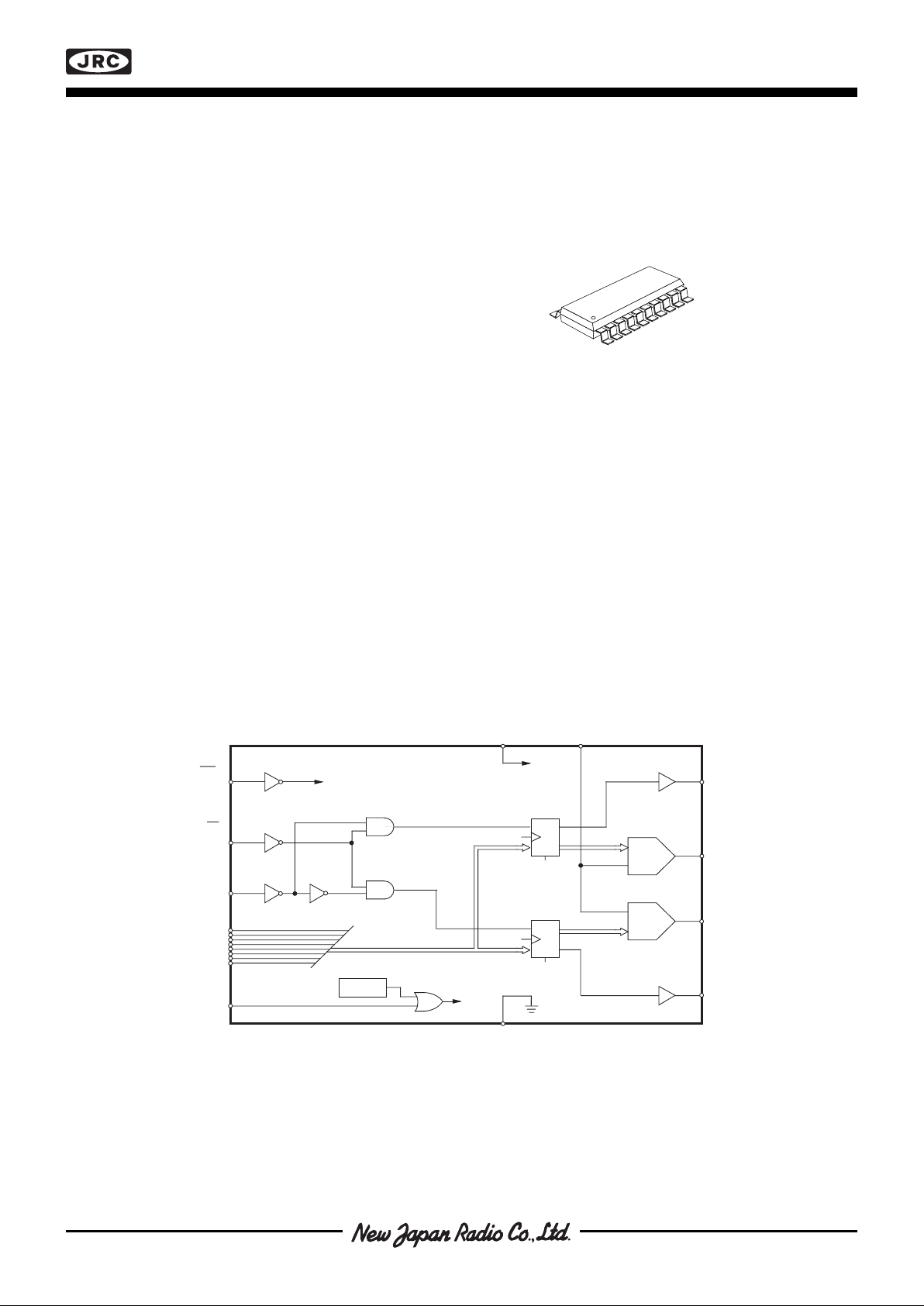
Figure 1. Block Diagram
V
DD
V
Ref
CS
A0
WR
D7 - D0
RESET
V
ss
Sign
2
DA
2
Sign
1
DA
1
D / A
D / A
E1
E2
POR
NJU39612
E
C
D
R
DA- Data 1
E
C
D
R
DA- Data 2
R
■ FEATURES
• Analog control voltages from 3V down to 0.0V
• High-speed microprocessor interface
• Full -scale error ±1 LSB
• Fast conversion speed 3 µs
• Matches the dual stepper motor drivers
• Package EMP20
■ BLOCK DIAGRAM
NJU39612E2
NJU39612 is a dual 7-bit+sign; Digital-to-Analog Converter
(DAC) developed to be used in micro stepping applications
together with the dual stepper motor driver. The NJU39612
has a set of input registers connected to an 8-bit data port for
easy interfacing directly to a microprocessor. Two registers
are used to store the data for each seven-bit DAC, the eighth
bit being a sign bit (sign/magnitude coding).
MICROSTEPPING MOTOR CONTROLLER WITH DUAL DAC
■ GENERAL DESCRIPTION ■ PACKAGE OUTLINE
NJU39612
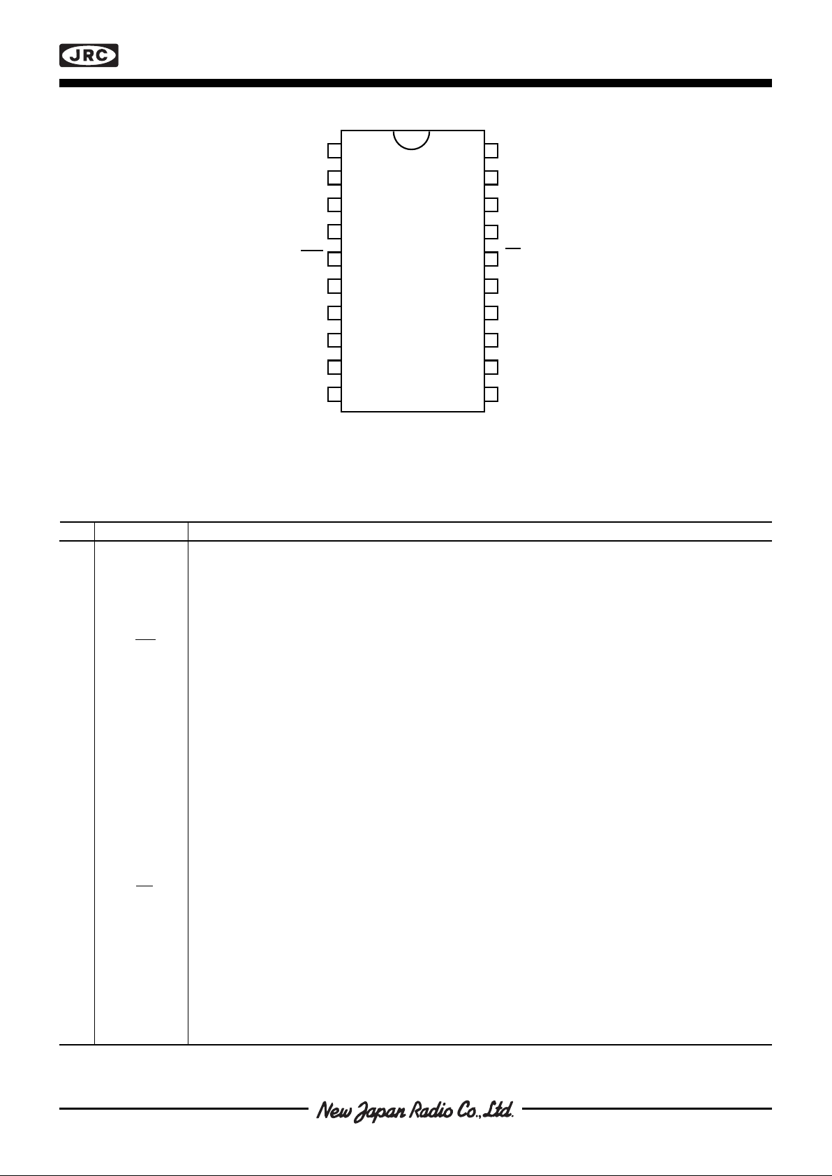
Figure 2. Pin configuration
1
2
3
4
5
6
7
8
9
10
18
17
16
15
14
13
12
11
D6
WR
D7
D4
D0
CS
A0
NC
V
ref
D5
DA
1
Sign
1
VDD
Reset
DA
2
Sign
2
V
ss
D3 D2
D1
19
20
NJU39612E2
■ PIN CONFIGURATION
■ PIN DESCRIPTION
Refer to figure 2.
EMP Symbol Description
1V
Ref
Voltage reference supply pin, 2.5 V nominal (3.0 V maximum)
2DA1Digital-to-Analog 1, voltage output. Output between 0.0 V and V
ref
- 1 LSB.
3 Sign
1
Sign 1, TTL/CMOS level. To be connected directly to NJM377x phase input. Databit D7 is transfered non
inverted from NJU39612 data input.
4V
DD
Voltage Drain-Drain, logic supply voltage. Normally +5 V.
5 WR Write, TTL/CMOS level, input for writing to internal registers. Data is clocked into flip flops on positive
edge.
6 D7 Data 7, TTL/CMOS level, input to set data bit 7 in data word.
7 D6 Data 6, TTL/CMOS level, input to set data bit 6 in data word.
8 D5 Data 5, TTL/CMOS level, input to set data bit 5 in data word.
9 D4 Data 4, TTL/CMOS level, input to set data bit 4 in data word.
10 D3 Data 3, TTL/CMOS level, input to set data bit 3 in data word.
11 D2 Data 2, TTL/CMOS level, input to set data bit 2 in data word.
12 D1 Data 1, TTL/CMOS level, input to set data bit 1 in data word.
13 D0 Data 0, TTL/CMOS level, input to set data bit 0 in data word.
14 A0 Address 0, TTL/CMOS level, input to select data transfer, A0 selects between cannel 1 (A0 = LOW) and
channel 2 (A0 = HIGH).
15 NC Not connected
16 CS Chip Select, TTL/CMOS level, input to select chip and activate data transfer from data inputs. LOW level
= chip is selected.
17 V
SS
Voltage Source-Source. Ground pin, 0 V reference for all signals and measurements unless otherwise
noted.
18 Sign
2
Sign 2. TTL/CMOS level. To be connected directly to NJM377x phase input. Data bit D7 is transfered
non-inverted from NJU39612 data input.
19 DA
2
Digital-to-Analog 2, voltage output. Output between 0.0 V and V
ref
- 1 LSB.
20 Reset Reset, digital input resetting internal registers. HIGH level = Reset, V
Res
≥ 3.5 V = HIGH level. Pulled low
internally.
NJU39612
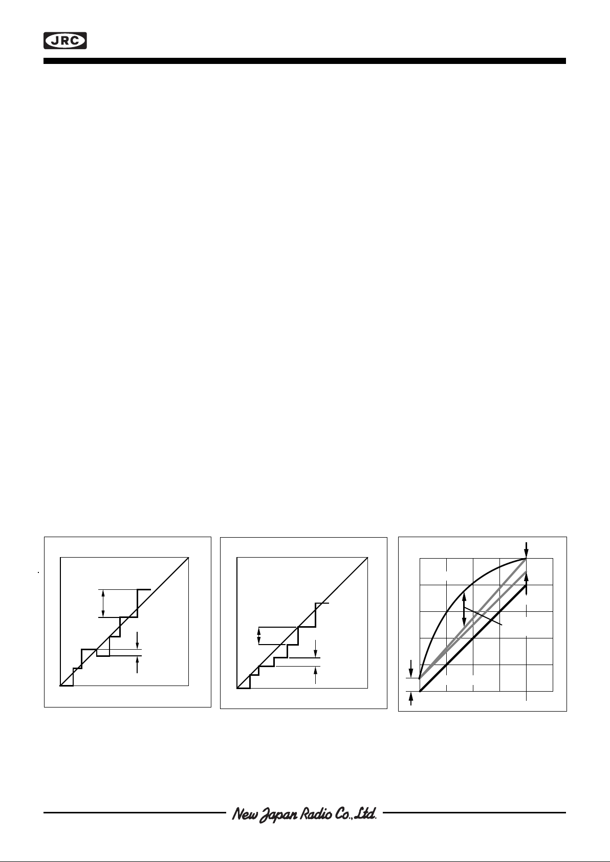
Endpoint
non-linearity
Offset error
Actual
Gain
error
Output
Input
Full scale
Correct
Less
than 2
bits
Positive
difference
Output
Input
More
than 2
bits
Negative
difference
Output
Input
Figure 5. Errors in D/A conversion.
Non-linearity, gain and offset errors.
Figure 4. Errors in D/A conversion.
Differential non-linearity of less than
1 bit, output is monotonic.
Figure 3. Errors in D/A conversion.
Differential non-linearity of more than
1 bit, output is non-monotonic.
■ DEFINITION OF TERMS
Resolution
Resolution is defined as the reciprocal of the number of discrete steps in the DAC output. It is directly related to the
number of switches or bits within the DAC. For example, NJU39612 has 27, or 128, output levels and therefor has 7
bits resolution. Remember that this is not equal to the number of microsteps available.
Linearity Error
Linearity error is the maximum deviation from a straight line passing through the end points of the DAC transfer
characteristic. It is measured after adjusting for zero and full scale. Linearity error is a parameter intrinsic to the
device and cannot be externally adjusted.
Power Supply Sensitivity
Power supply sensitivity is a measure of the effect of power supply changes on the DAC full-scale output.
Settling Time
Full-scale current settling time requires zero-to-full-scale or full-scale-to-zero output change. Settling time is the
time required from a code transition until the DAC output reaches within ±1/2LSB of the final output value.
Full-scale Error
Full-scale error is a measure of the output error between an ideal DAC and the actual device output.
Differential Non-linearity
The difference between any two consecutive codes in the transfer curve from the theoretical 1LSB, is differential
non-linearity
Monotonic
If the output of a DAC increases for increasing digital input code, then the DAC is monotonic. A 7-bit DAC which is
monotonic to 7 bits simply means that increasing digital input codes will produce an increasing analog output.
NJU39612 is monotonic to 7 bits.
■ FUNCTIONAL DESCRIPTION
Each DAC channel contains one register and a D/A converter. A block diagram is shown on the first page.
The sign outputs generate the phase shifts, i.e., they reverse the current direction in the phase windings.
Data Bus Interface
NJU39612 is designed to be compatible with 8-bit microprocessors such as the 6800, 6801, 6803, 6808, 6809,
8051, 8085, Z80 and other popular types and their 16/32 bit counter parts in 8 bit data mode. The data bus interface consists of 8 data bits, write signal, chip select, and two address pins. All inputs are TTL-compatible (except
reset). The address pin control data transfer to the two internal D-type registers. Data is transferred according to
figure 7 and on the positive edge of the write signal.
NJU39612
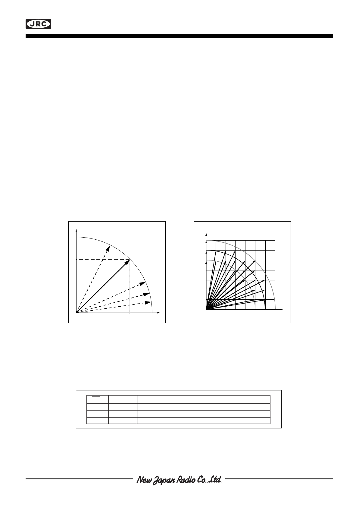
T [mNm]
1
T [mNm]
2
max
T
nom
T
min
T
I [mA]
1
I [mA]
2
I
CS A0 Data Transfer
0 0 D7 —> Sign1, (D6—D0) —> (Q61—Q01)
0 1 D7 —> Sign2, (D6—D0) —> (Q62—Q02)
1 X No Transfer
Current Direction, Sign1 & Sign
2
These bits are transferred from D7 when writing in the respective DA register. A0 must be set according to the data
transfer table in figure 7.
DA1 and DA
2
These are the two outputs of DAC1 and DAC2. Input to the DACs are internal data bus (Q61 … Q01) and (Q62 … Q02).
Reference Voltage V
Ref
V
Ref
is the analog input for the two DACs. Special care in layout, gives a very low voltage drop from pin to resistor.
Any V
Ref
between 0.0 V and VDD can be applied, but output might be non-linear above 3.0 V.
Power-on Reset
This function automatically resets all internal flip flops at power-on. This results in VSS voltage at both DAC outputs
and all digital outputs.
Reset
If Reset is not used, leave it disconnected. Reset can be used to measure leakage currents from VDD.
Figure 7. Table showing how data is transfered inside NJU39612.
Figure 6b. An example of accessible positions with a given torque
deviation/fullstep. Note that 1:st
µstep sets highest resolution. Data
points are exaggerated for illustration purpose.
TNom = code 127.
Figure 6a. Assuming that torque is
proportional to the current in resp.
winding it is possible to draw figure
8b.
 Loading...