

JRC NJU3554L, NJU3554FA1 Datasheet
NJU3554
4-BIT SINGLE CHIP OTP MICRO CONTROLLER
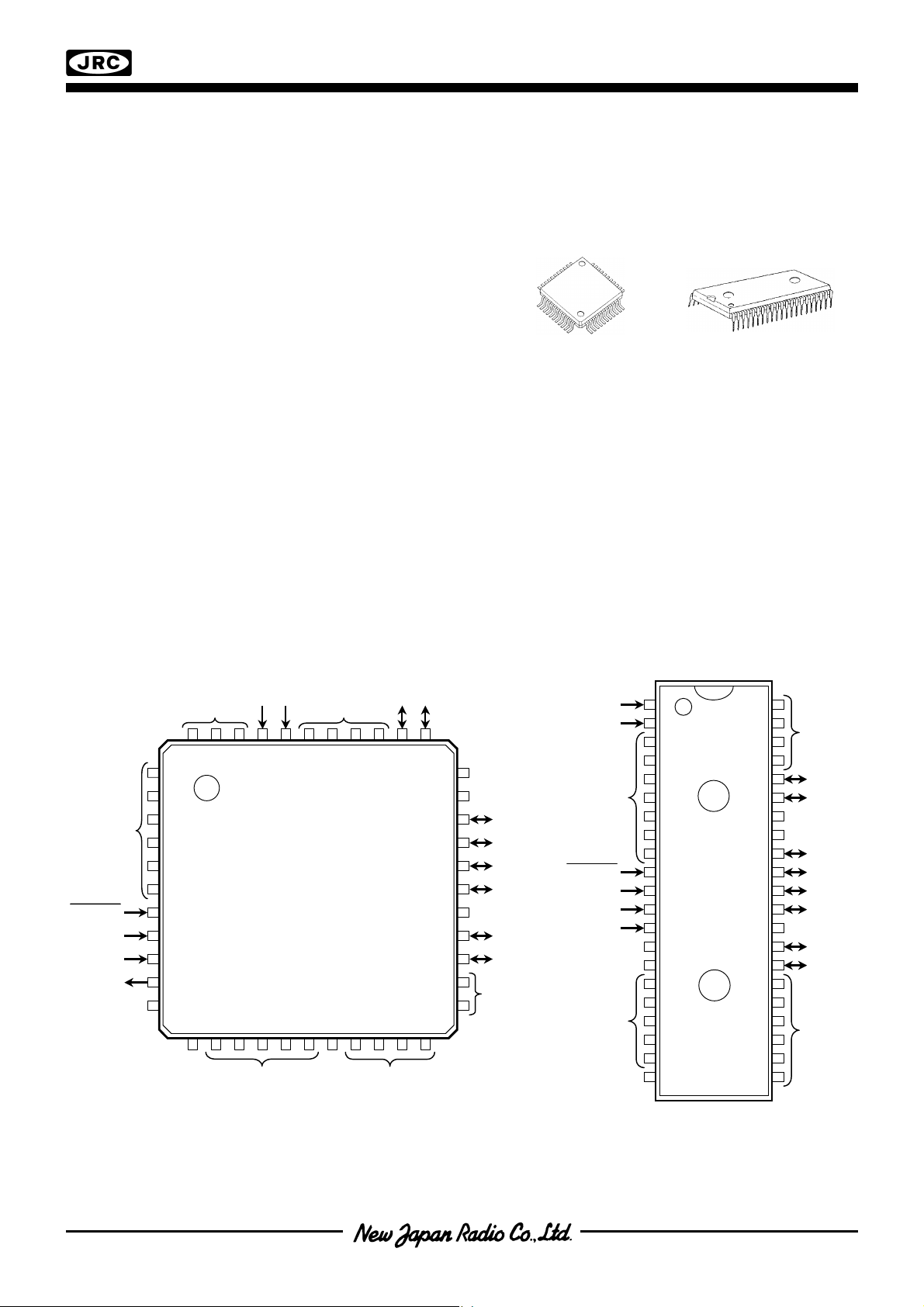
PACKAGE OUTLINE
GENERAL DESCRIPTION
■
NJU3554
The
is the C-MOS 4-bit Single Chip OT P type
Micro Controller with programmable Flash Memory.
It is completely compatible with the
and the pin configuration. Therefore, the
suitable for the final evaluation before
NJU3504
NJU3504
in function
NJU3554
mask
generation, the small quantity production and short leadtime.
* In this data sheet, only OTP programming and the
difference between NJU3554 and NJU3504 are
mentioned mainly.
Therefore the detail function and specification should
be referred on the NJU3504 data sheet.
FEATURES
■
●
Internal One Time Programmable ROM 4,096 X 8bits
●
Internal Data RAM 256 X 4bits
●
Wide operating voltage range 2.7V ~ 5.5V
●
Package outline QFP44-A1 / SDIP42 (Compatible with
●
ROM programmer “SUPERPRO/L” by XELTEK co,.
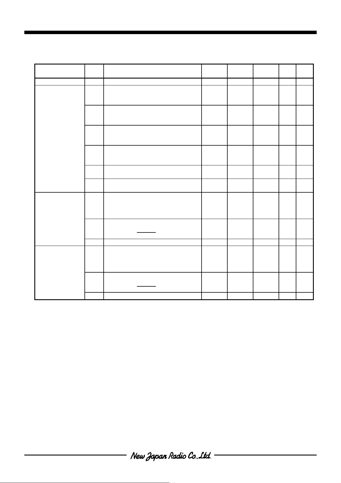
PIN CONFIGURATION IN OTP PROGRAMMING MODE
■
■
is
NJU3554FA1 NJU3554L
PRELIMINARY
NJU3504
)
Open
RESET
PROM
CLK
REQ
[ QFP44-A1 ]
D6
37
19
36
20
D7
35
21
Open
34
33
32
31
30
29
28
27
26
25
24
23
22
V
DD
Open
D5
D4
D3
D2
Open
D1
D0
Open
CNT1
44
Open
43
42
CNT2
41
40
39
Open
38
1
2
3
4
5
6
NJU3554FA1
7
8
9
10
SS
11
12
13
14
15
16
17
18
SS
V
V
DD
V
Open
Note) The pin configuration in Normal operating mode is the same as
[ SDIP42 ]
CNT1
CNT2
Open
RESET
PROM
CLK
REQ
Open
V
SS
V
SS
V
DD
NJU3504
1
2
3
4
5
6
7
8
9
10
11
12
13
14
15
16
17
18
19
20
42
41
40
39
38
37
36
35
34
33
32
31
30
NJU3554L
29
28
27
26
25
24
23
21 22
.
Open
D7
D6
V
DD
Open
D5
D4
D3
D2
Open
D1
D0
Open
- 1 -
NJU3554
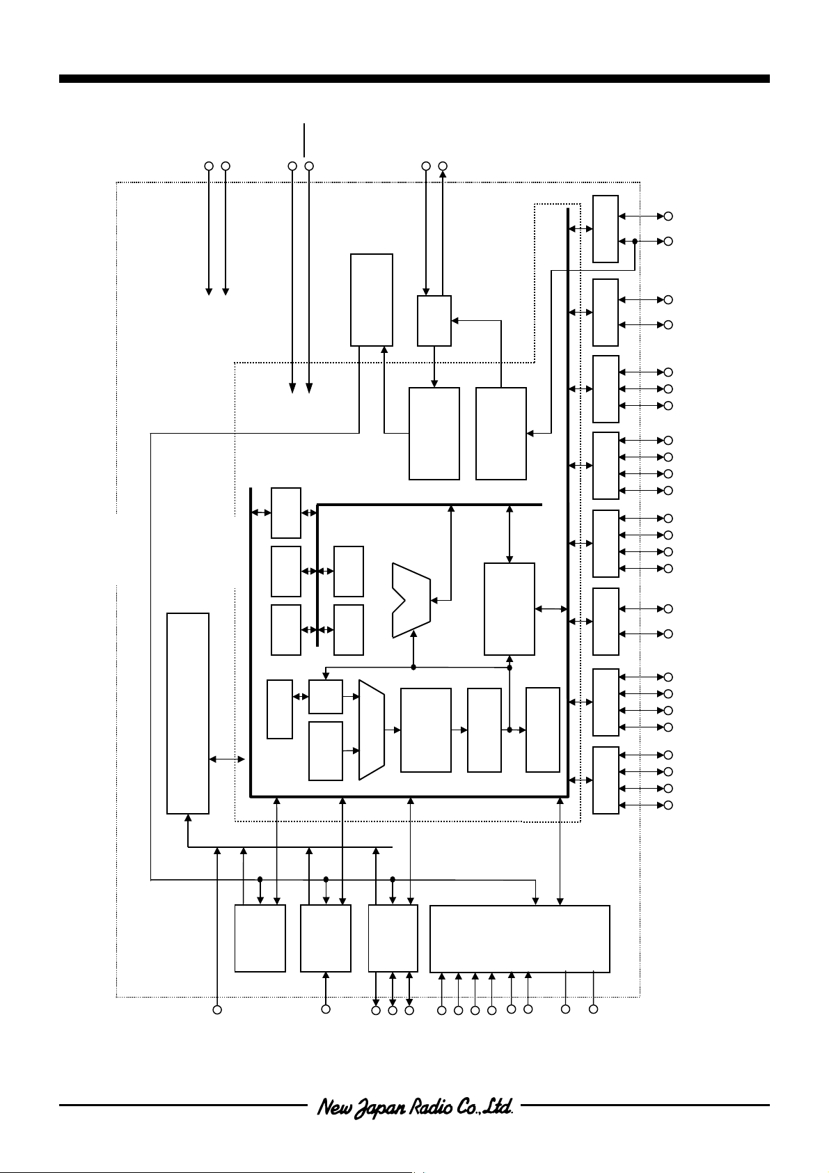
BLOCK DIAGRAM
■
NJU3554
DD
SS
V
V
CPU CORE
TEST
AC Y Reg X Reg
RESET
PRESCALER
Y’ Reg X’ Reg
PC
STACK
MUX
Interrupt Logic
INT2
INT1
TIMER1
EXTI/PK0
INT3
TLU addr
TIMER2
CNTI/PK1
INT4
SDO/PL0
SIO
SDI(O)/PL1
OSC1
CPU
ALU
OTP ROM
OSC2
OSC
TIMING
GENERATOR
4096 x 8 bits
AIN1/PI1
AIN0/PI0
PH1
PORT_H
PORT_G
PORT_F
STANDBY
CONTROLLER
PORT_E
PORT_D
RAM
256 x 4 bits
I R
AIN2/PI2
AIN3/PI3
I D
A/D
/PJ0
REF
V
ADCK/PJ1
AV
PORT_C
PORT_B
PORT_A
DD
AVss
PH0
PG1
PG0
PF2
PF1
PF0
PE3
PE2
PE1
PE0
PD3
PD2
PD1
PD0
PC1
PC0
PB3
PB2
PB1
PB0
PA3
PA2
PA1
PA0
Refer [INPUT OUTPUT TERMINAL TYPE]
*
- 2 -
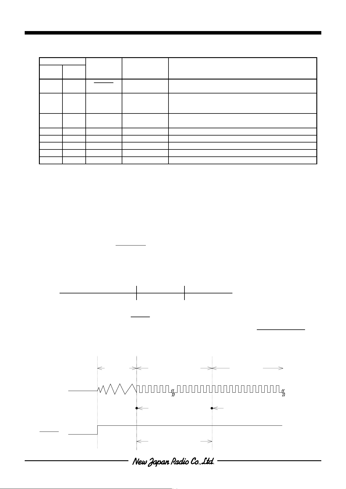
TERMINAL DESCRIPTION IN OTP PROGRAMMING MODE
■
NJU3554
No.
NJU
3554F
NJU
3554L
SYMBOL
7 10 RESET INPUT
25, 26,
28-31,
34, 35
28, 29,
31-34,
37, 38
D0 - D7 INPUT/OUTPUT Data bus
1 40, CNT1 INPUT
2 41 CNT2 INPUT
INPUT /
OUTPUT
F U N C T I O N
RESET terminal.
When the low-level input-signal, the system is initialized.
OTP control input terminal
10 13 REQ OUTPUT Request output terminal
9 12 CLK INPUT Clock input terminal
8 11 PROM INPUT OTP programming enable terminal
18, 33 21, 36 VDD - Power Source (5V)
11, 12 14, 15 VSS - Power Source (0V)
Note 1) Use at V
=5V in OTP programming mode.
DD
2) Non connect anything to the other terminals.
Difference between NJU3554 (OTP version) and NJU3504 (MASK version)
■
●
Operating mode
NJU3554
mode”.
•
Normal operating mode
has two operating modes. One is ”Normal operating mode” and the other is “OTP programm ing
The ”TEST” terminal is set to low level. (The terminal is recommended to connect to GND.)
Operating voltage range; 2.7V ~ 5.5V
•
OTP Programming mode
.
User program is read out from or written into the OTP by the universal programmer “SUPERPRO/ L” and
converting adapter made by XELTEK co,.(USA).
●
Reset Terminal Type
NJU3554 NJU3504
Internal Pull-up Resistance
With Pull-up
Without Pull-up
●
Option information set in the initialization
When the initialization is perf orm ed(RESET ter m inal is “L” ), the operation inf orm ation stor ed in option area is
OSC
set as shown in the following timing chart . The option information is set in the term of
1 / f
x 512clock
RESET releasing and oscillation stability time. Af ter inform ation set, the progr am c ounter is set to 0000H and
NJU3554
the
operates in normal.
[ TIMING CHART ]
Oscillation
Stability
Time
Option information setting
x512clock
1/f
OSC
Normal
Operation
Oscillator
Clock
Oscillation
Start
PC=0000H
RESET
f
=4MHz
OSC
about 128µsec
after
- 3 -
NJU3554
ABSOLUTE MAXIMUM RATINGS
■
(Ta=25°C)
PARAMETER SYMBOL RATINGS UNIT
Supply Voltage VDD -0.3 ~ +7.0 V
Input Voltage VIN -0.3 ~ V
Output Voltage V
-0.3 ~ V
OUT
Analog Supply Voltage AVDD -0.3 ~ V
Analog Reference Voltage V
-0.3 ~ AV
REF
Analog Input Voltage AIN0 ~ AIN3 -0.3 ~ AV
Operating Temperature
Storage Temperature
T
-20 ~ +75
opr
T
-55 ~ +125
stg
+ 0.3 V
DD
+ 0.3 V
DD
+ 0.3 V
DD
+ 0.3 V
DD
+ 0.3 V
DD
°
C
°
C
Note)
The difference of electrical characteristics between
NJU3554
(OTP version) and
NJU3504
(MASK version)
NJU3504 NJU3554
•
Supply Voltage (VDD) MIN.
2.4V
→
2.7V
•
Supply Current
5V (I
(I
(I
(I
(I
DD1
DD2
DD3
DD4
DD5
) Max.
) Max.
) Max.
) Max.
) Max.
4.0mA
4.0mA
3.8mA
5.2mA
4.0µA
→
→
→
30mA
30mA
30mA
30mA
20µA
→
3V (I
(I
(I
(I
(I
DD1
DD2
DD3
DD4
DD5
) Max.
) Max.
) Max.
) Max.
) Max.
2.0mA
2.0mA
1.8mA
1.4mA
2.0µA
→
→
20mA
20mA
20mA
→
→
20mA
20µA
- 4 -
NJU3554
ELECTRICAL CHARACTERISTICS DC CHARACTERISTICS 1-1
■
(VDD=3.6~5.5V, VSS=0V, Ta=-20~75°C)
PARAMETER
Supply Voltage VDD VDD 3.6 5.5 V
Supply Current
High-Level
Input Voltage
Low-level
Input Voltage
*1 Input/output port is set as an Input terminal.
*2 Input/output port is set as an Output terminal.
*3 Except the current through Pull-up resister.
SYM
BOL
I
DD1
V
V
C O N D I T I O N S MIN TYP MAX UNIT NOTE
DD
DD
=5V, f
OSC
=2MHz
30 mA *3
X’tal Oscillation in Reset
V
I
DD2
DD
V
DD
=5V, f
OSC
=2MHz
30 mA *3
Ceramic Oscillation in Reset
V
I
DD3
DD
V
DD
=5V, f
OSC
=2MHz
30 mA *3
CR Oscillation in Reset
V
I
DD4
DD
V
DD
=5V, f
OSC
=4MHz
30 mA *3
Operating (Except ADC)
V
I
DD5
I
ADD
DD
=5V, STANDBY Mode
V
DD
AV
AV
DD
DD=VDD
=5V, ADCK=225kHz
20
µ
A
3.0 5.0 mA *3
PA0~PA3, PB0~PB3, PC0, PC1,
PD0~PD3, PE0~PE3,
V
IH1
AIN0/PI0~AIN3/PI3, SDI(O)/PL1,
VDD V *1
0.7V
DD
SCK/CKOUT
PF0~PF2, PG0, PG1, PH0, PH1,
V
V
IH2
/PJ0, ADCK/PJ1, EXTI/PK0,
REF
0.8VDD VDD V *1
CNTI/PK1, RESET
OSC1 VDD-1.0 VDD V
V
IH3
PA0~PA3, PB0~PB3, PC0, PC1,
PD0~PD3, PE0~PE3,
V
IL1
AIN0/PI0~AIN3/PI3, SDI(O)/PL1,
0 0.3V
V *1
DD
SCK/CKOUT
PF0~PF2, PG0, PG1, PH0, PH1,
V
V
IL2
/PJ0, ADCK/PJ1, EXTI/PK0,
REF
0 0.2VDD V *1
CNTI/PK1, RESET
OSC1 0 1.0 V
V
IL3
*3
- 5 -
NJU3554
ELECTRICAL CHARACTERISTICS DC CHARACTERISTICS 1-2
■
PARAMETER
High-Level
Input Current
Low-Level
Input Current
High-Level
Output Voltage
Low-Level
Output Voltage
Output
Leakage
Current
Input Capacitance CIN
*1 Input/output port is set as an Input terminal.
*2 Input/output port is set as an Output terminal.
*3 Except the current through Pull-up resister.
SYM
BOL
V
C O N D I T I O N S MIN TYP MAX UNIT NOTE
=5.5V, VIN=5.5V
DD
PA0~PA3, PB0~PB3, PC0, PC1,
PD0~PD3, PE0~PE3, PF0~PF2,
I
PG0, PG1, PH0, PH1,
IH
AIN0/PI0~AIN3/PI3, V
ADCK/PJ1, EXTI/PK0, CNTI/PK1,
SDI(O)/PL1, RESET, SCK/CKOUT
VDD=5.5V, VIN=0V
Without pull-up resistance
PA0~PA3, PB0~PB3, PC0, PC1,
PD0~PD3, PE0~PE3, PF0~PF2,
I
IL1
PG0, PG1, PH0, PH1,
AIN0/PI0~AIN3/PI3, V
ADCK/PJ1, EXTI/PK0, CNTI/PK1,
SDI(O)/PL1, SCK/CKOUT
VDD=5.5V, VIN=0V
With pull-up resistance
PA0~PA3, PB0~PB3, PC0, PC1,
PD0~PD3, PE0~PE3, PF0~PF2,
I
IL2
PG0, PG1, PH0, PH1,
AIN0/PI0~AIN3/PI3, V
ADCK/PJ1, EXTI/PK0, CNTI/PK1,
SDI(O)/PL1, RESET, SCK/CKOUT
I
=-100µA
OH
PD0~PD3, PE0~PE3, PF0~PF2,
V
OH
PG0, PG1, PH0, PH1, SDO/PL0,
SDI(O)/PL1, SCK/CKOUT
I
=400µA
OL1
PD0~PD3, PE0~PE3, PF0~PF2,
V
OL1
PG0, PG1, PH0, PH1, SDO/PL0,
SDI(O)/PL1, SCK/CKOUT
I
=15mA
OL2
V
OL2
PA0~PA3, PB0~PB3, PC0, PC1
=5.5V, VOH=5.5V
V
DD
I
OD
PA0~PA3, PB0~PB3, PC0, PC1
Except V
=1MHz
f
OSC
, VSS terminals
DD
Other terminals : 0V
REF
REF
REF
/PJ0,
/PJ0,
/PJ0,
V
DD
(VDD=3.6~5.5V, VSS=0V, Ta=-20~75°C)
10
-10
-100
µ
µ
µ
A
A
A
*1
*1
*1
-0.5 V *2
0.5 V *2
2.0 V *2
10
µ
A
*2
10 20 pF
- 6 -
 Loading...