

JRC NJU3151M, NJU3151D Datasheet
NJU3151
4-BIT SINGLE CHIP OTP TINY CONTROLLER
GENERAL DESCRIPTION
■
NJU3151
The
Micro Controller with programmable Flash Memory.
It is completely compatible with the
and the pin configuration. Therefore, the
suitable for the final evaluation before
generation, the small quantity production and short leadtime.
* In this data sheet, only OTP programming and the
difference between NJU3151 and NJU3101 are
mentioned mainly.
Therefore the detail function and specification should
be referred on the NJU3101 data sheet.
FEATURES
■
●
Internal One Time Programmable ROM 512 X 8bits
●
Internal Data RAM 16 X 4bits
●
Wide operating voltage range 2.7V ~ 5.5V
●
Package outline DIP16 / DMP16
●
ROM programmer “SUPERPRO/L” by XELTEK co,.
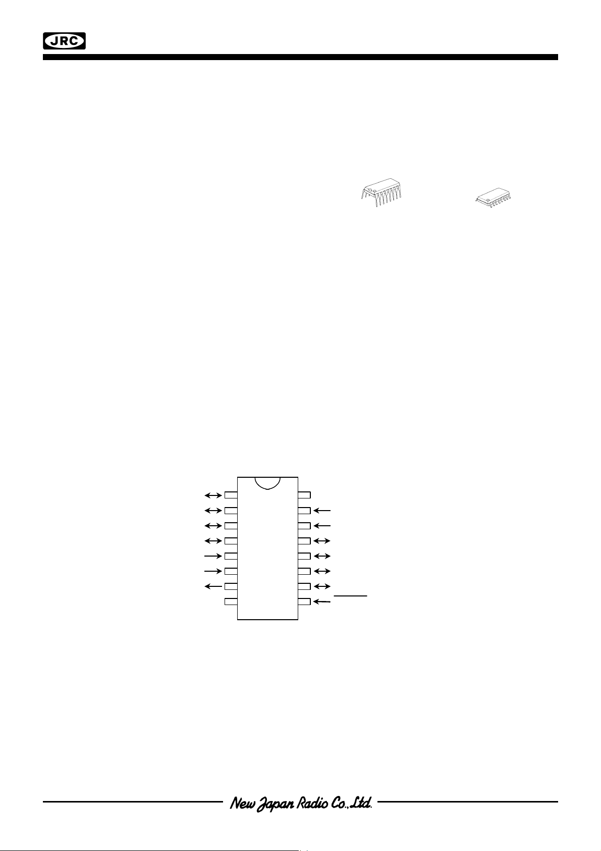
PIN CONFIGURATION IN OTP PROGRAMMING MODE
■
is the C-MOS 4-bit Single Chip OT P type
NJU3101
in function
NJU3151
NJU3101
mask
is
PRELIMINARY
PACKAGE OUTLINE
■
NJU3151D NJU3151M
Note) The pin configuration in Normal operating mode is the same as
D0
D1
D2
D3 D7
PROM
CLK
REQ
V
SS
1
2
3
4
5
6
7
8 9
16
15
14
13
12
11
10
V
DD
CNT2
CNT1
D6
D5
D4
RESET
NJU3101
.
- 1 -
NJU3151
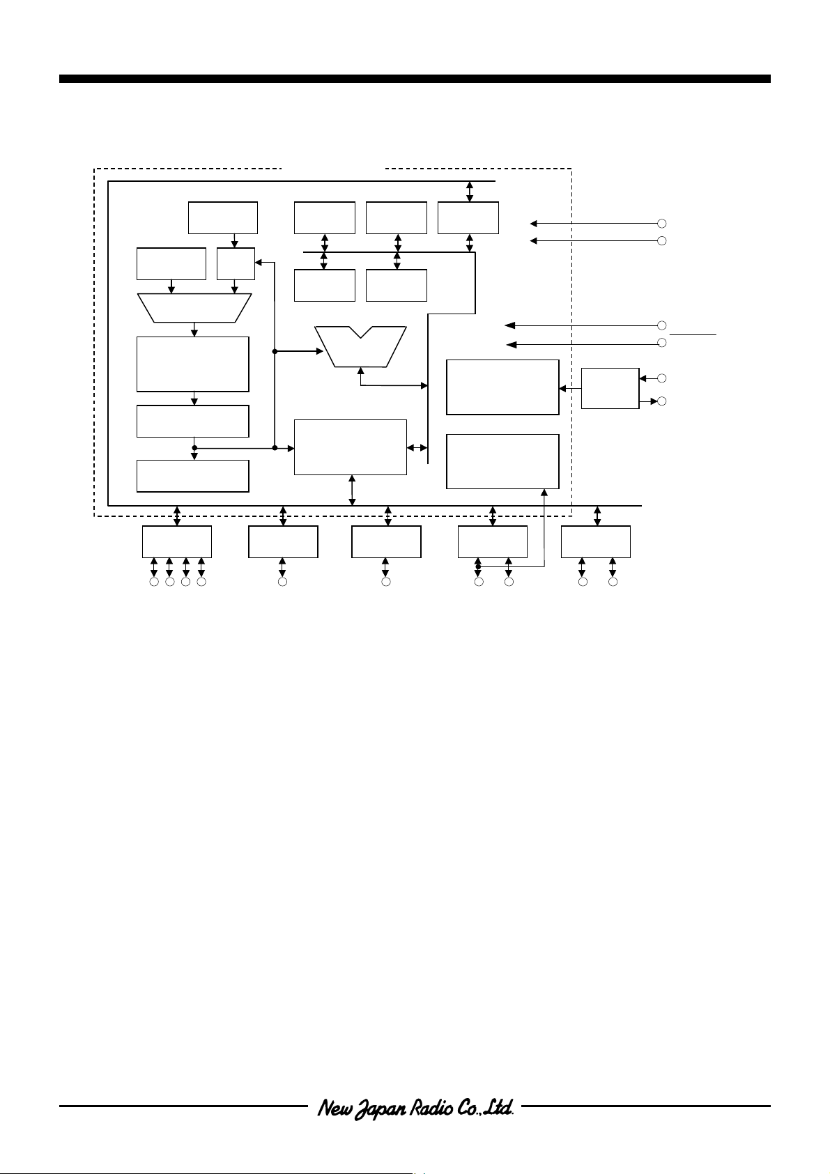
BLOCK DIAGRAM
■
TLUaddr
OTP ROM
512 x 8 bit
PA0
MUX
I R
I D
PA1
PA2
STACK
PC
PA3
PORT_B PORT_A
CPU CORE
RAM
16 x 4 bit
PB0
ALU
Y’-Reg X’-Reg
PC0
AC Y-Reg X-Reg
CPU
TIMING
GENERATOR
STANDBY
CONTROLLER
PD0
PD1
V
DD
V
SS
TEST
RESET
OSC
PORT_E PORT_D PORT_C
PE0
PE1
OSC1
OSC2
- 2 -
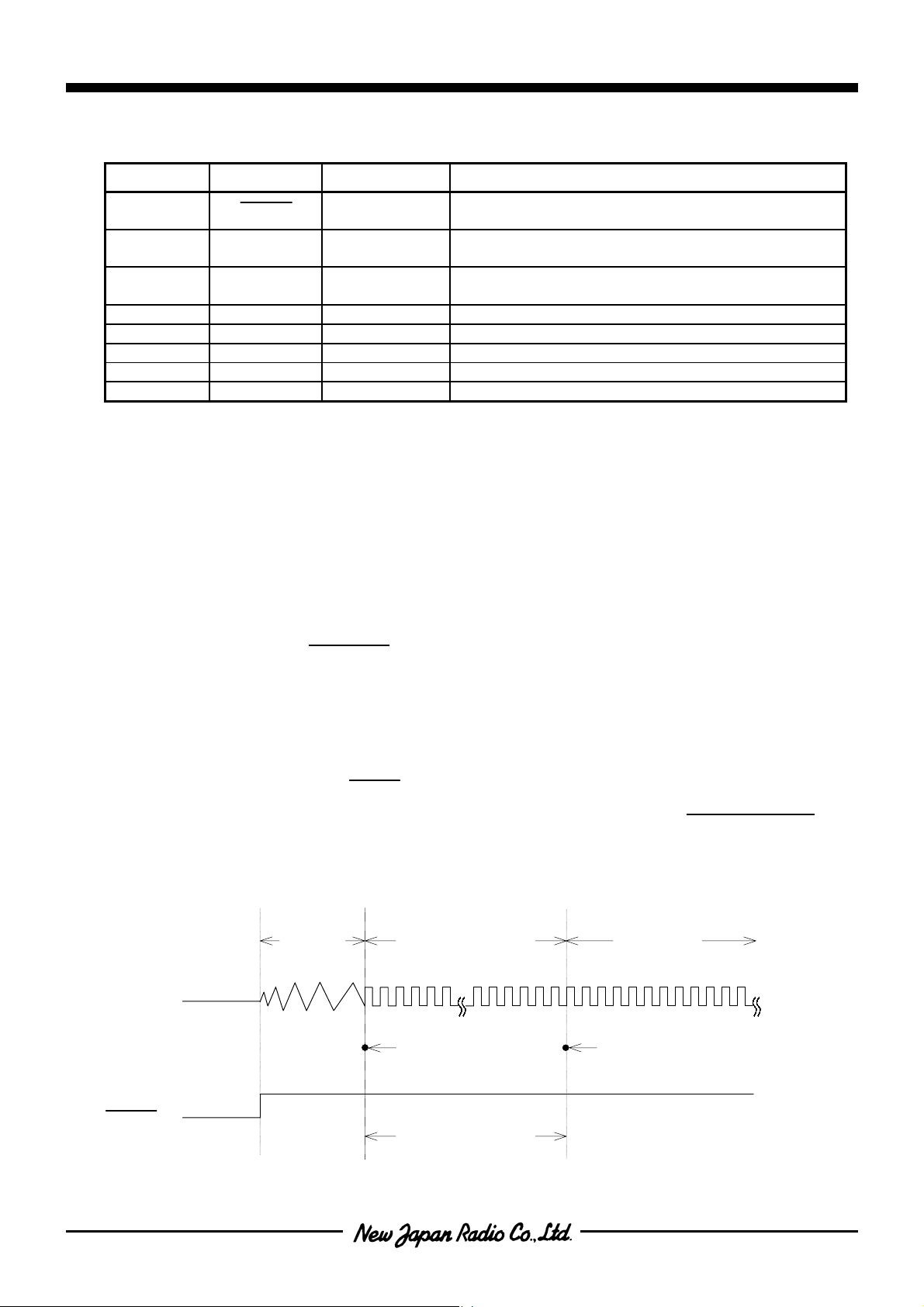
TERMINAL DESCRIPTION IN OTP PROGRAMMING MODE
■
No. SYMBOL INPUT/OUTPUT F U N C T I O N
9 RESET INPUT
1 - 4,
10 - 13,
D0 - D7 INPUT/OUTPUT Data bus
14, CNT1 INPUT
15 CNT2 INPUT
RESET terminal.
When the low-level input-signal, the system is initialized.
OTP control input terminal
7 REQ OUTPUT Request output terminal
6 CLK INPUT Clock input terminal
5 PROM INPUT OTP programming enable terminal
16 VDD - Power Source (5V)
8 VSS - Power Source (0V)
Note 1) Use at V
=5V in OTP programming mode.
DD
2) Non connect anything to the other terminals.
Difference between NJU3151 (OTP version) and NJU3101 (MASK version)
■
NJU3151
●
Operating mode
NJU3151
has two operating modes. One is ” Normal operating m ode” and the other is “OTP programming
mode”.
•
Normal operating mode
The ”TEST” terminal is set to low level. (The terminal is recommended to connect to GND.)
Operating voltage range; 2.7V ~ 5.5V
.
•
OTP Programming mode
User program is read out from or written into the OTP by the universal programmer “SUPERPRO/ L” and
converting adapter made by XELTEK co,.(USA).
●
Option information set in the initialization
When the initialization is perf orm ed(RESET ter m inal is “L” ), the operation inf orm ation stor ed in option area is
OSC
set as shown in the following timing chart . The option information is set in the term of
1 / f
x 256clock
RESET releasing and oscillation stability time. After information set, the program counter is set to 0000H and
NJU3151
the
operates in normal.
[ TIMING CHART ]
Oscillation
Stability
Time
Option information setting
x256clock
1/f
OSC
Normal
Operation
Oscillator
Clock
Oscillation
Start
PC=0000H
RESET
f
=4MHz
OSC
about 64µsec
after
- 3 -
NJU3151
ABSOLUTE MAXIMUM RATINGS
■
(Ta=25°C)
PARAMETER SYMBOL RATINGS UNIT
Supply Voltage VDD -0.3 ~ +7.0 V
Input Voltage VIN -0.3 ~ V
Output Voltage V
Operating Temperature
Storage Temperature
-0.3 ~ V
OUT
T
-20 ~ +75
opr
-55 ~ +125
T
stg
+ 0.3 V
DD
+ 0.3 V
DD
°
C
°
C
Note)
The difference of electrical characteristics between
NJU3151
(OTP version) and
NJU3101
(MASK version)
NJU3101 NJU3151
•
Supply Voltage (VDD) MIN.
2.4V
→
2.7V
•
Supply Current
5V (I
(I
(I
(I
DD1
DD2
DD3
DD4
) Max.
) Max.
) Max.
) Max.
4.0mA
4.0mA
3.8mA
4.0µA
→
→
→
30mA
30mA
30mA
20µA
3V (I
(I
(I
(I
DD1
DD2
DD3
DD4
) Max.
) Max.
) Max.
) Max.
2.0mA
2.0mA
1.8mA
2.0µA
→
→
20mA
20mA
20mA
20µA
→
- 4 -
 Loading...