

DUAL CONTROLLER FOR HIGH-CURRENT STEPPER MOTOR
■ GENERAL DESCRIPTION ■ PACKAGE OUTLINE
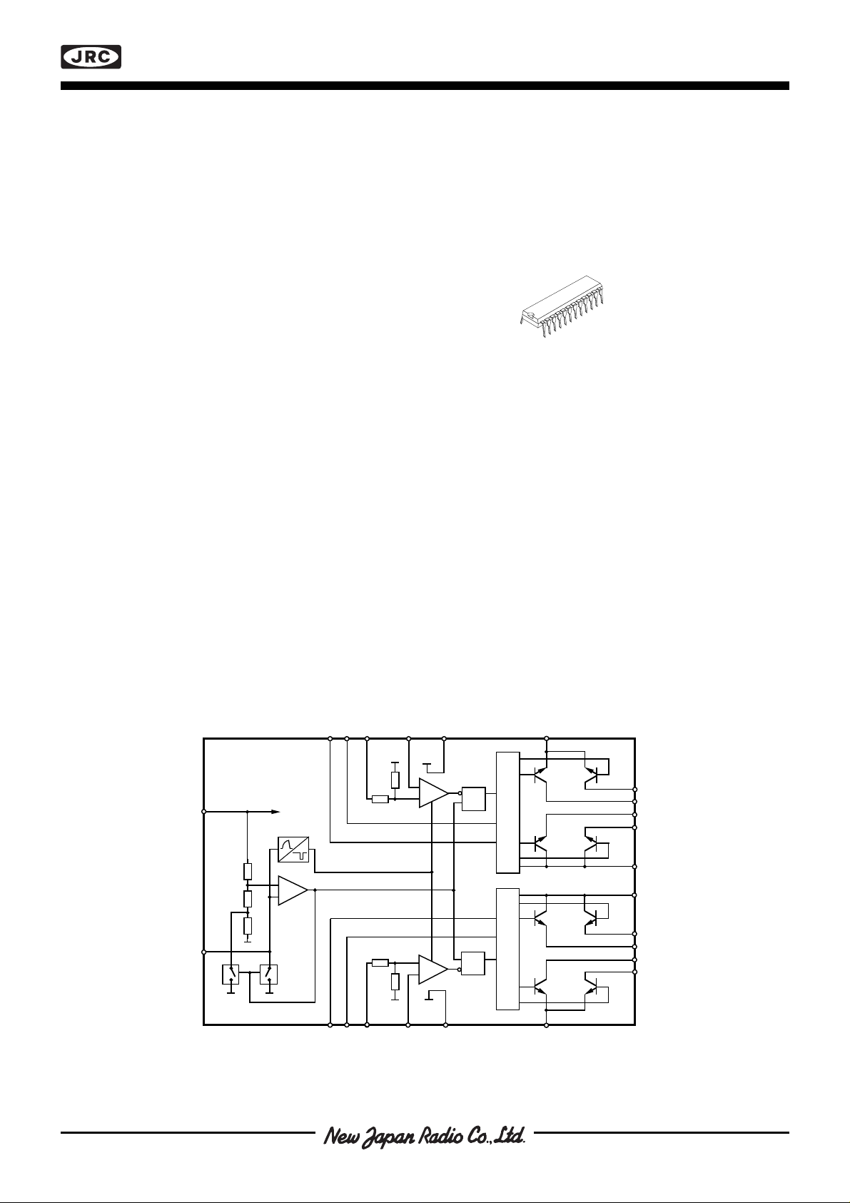
The NJM3776 is a switch-mode (chopper), constant-current
controller intended for controlling external transistors in a high
current stepper motor application. The NJM3776 has two channels,
one for each winding of a two-phase stepper motor. The NJM3776
is equipped with a Disable input to simplify half stepping operation.
The NJM3776 contains a clock oscillator, which is common for both
driver channels, a set of comparators and flip-flops implementing
the switching control, and two output sections each containing four
outputs, two source and two sink, intended to drive an external Hbridge. Voltage supply requirements are +5 V for logic and +10 to
+45 V for the outputs.
NJM3776D2
NJM3776
■ FEATURES
• Suitable to drive any external MOS FET or bipolar power transistor
• Cross conduction prevented by time delay
• Digital filter on chip eliminates external filtering components
• Package DIP24
■ BLOCK DIAGRAM
C
V
1
R1
–
+
V
CC
NJM3776
Phase
V
CC
+
–
Dis
1
1
SGND
Pwr GND
1
Q
R
S
Logic
1
1
T
1BL
T
1AL
T
1AU
T
1BU
V
BB1
V
BB2
RC
Figure 1. Block diagram
Phase
T
Logic
+
C
V
Dis
2
2
2
R2
SRQ
–
SGND
Pwr GND
2
2
2BU
T
2AU
T
2AL
T
2BL
■ PIN CONFIGURATION
NJM3776
PWR GND
T1BL
T1BU
T1AL
T1AU
VBB1
SGND
VR
Phase
Dis
1
1
2
3
4
5
6
NJM
7
1
3776D2
8
1
C
9
1
10
1
11
1
RC Vcc
12 13
PWR GND
24
T2BL
23
22
T2BU
T2AL
21
T2AU
20
VBB 2
19
SGND
18
VR
17
C
16
2
Phase
15
Dis
14
2
2
2
2
2
Figure 2. Pin configuration
■ PIN DESCRIPTION
DIP Symbol Description
1 PWR GND 1"Power Ground" from output channel 1. Connected to the ground path (see application examples).
2 T1BL Output, channel 1, B side lower transistor. The pin will sink current when phase is high.
3 T1BU Output, channel 1, B side upper transistor. The pin will source current when phase is low.
4 T1AL Output, channel 1, A side lower transistor. The pin will sink current when phase is low.
5 T1AU Output, channel 1, A side upper transistor. The pin will source current when phase is high.
6 VBB1 Supply voltage for driving channel 1 outputs.
7 SGND
8VR
9C
10 Phase
11 Dis
1
1
1
1
1
12 RC Clock oscillator RC pin. Connect a 12 kohm resistor to V
13 Vcc Logic voltage supply, nominally +5 V.
14 Dis
15 Phase
16 C
17 VR
18 SGND
2
2
2
2
2
19 VBB2 Supply voltage for driving channel 2 outputs.
20 T2AU Output, channel 2, A side upper transistor. The pin will source current when phase is high.
21 T2AL Output, channel 2, A side lower transistor. The pin will sink current when phase is low.
22 T2BU Output, channel 2, B side upper transistor. The pin will source current when phase is low.
23 T2BL Output, channel 2, B side lower transistor. The pin will sink current when phase is high.
24 PWR GND
Sense ground channel 1. Logic ground reference and sense ground for the current control feedbackloop.
Reference voltage, channel 1. Controls the comparator threshold voltage and hence the output
current.
Comparator input channel 1. This input senses the instantaneous voltage across the sensing resistor,
filtered by the internal digital filter or an optional external RC network.
Controls the direction of channel 1 outputs T1AL, T1AU, T1BL and T1BU.
Disable input for channel 1. When HIGH, all four output transistors are turned off, which results in a
rapidly decreasing output current to zero.
and a 4 700 pF capacitor to ground to
CC
obtain the nominal switching frequency of 23.0 kHz and a digital filter blanking time of 1.0 µs.
Disable input for channel 2. When HIGH, all four output transistors are turned off, which results in a
rapidly decreasing output current to zero.
Controls the direction of channel 2 outputs T2AL, T2AU, T2BL and T2BU.
Comparator input channel 2. This input senses the instantaneous voltage across the sensing resistor,
filtered by the internal digital filter or an optional external RC network.
Reference voltage, channel 2. Controls the comparator threshold voltage and hence the output
current.
Sense ground channel 1. Logic ground reference and sense ground for the current control feedbackloop.
"Power Ground" from output channel 2. Connected to the ground path (see application examples).
2
NJM3776
■ FUNCTIONAL DESCRIPTION
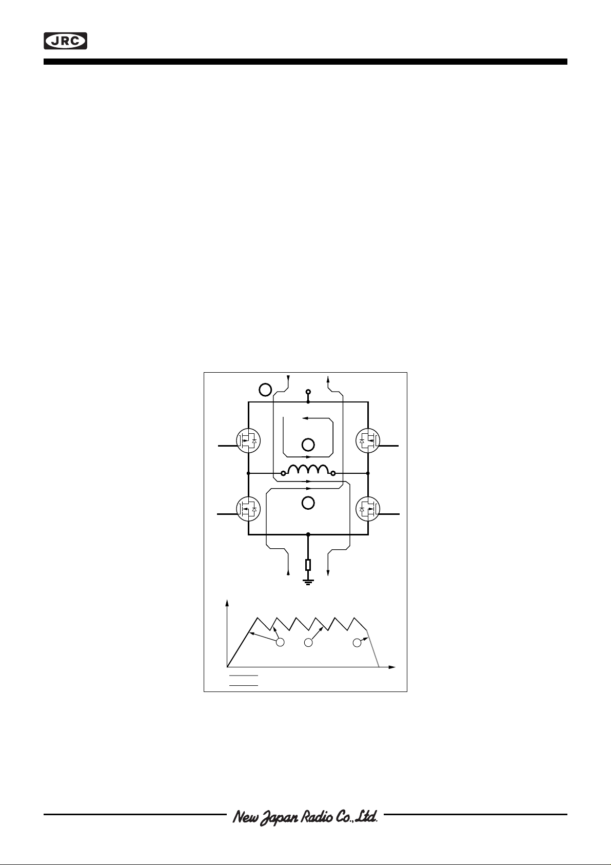
Each channel of the NJM3776 consists of the following sections:
• An output section with four output transistors, two sourcing and two sinking, intended to drive the four transistors
in an external H-bridge. Each transistor is capable of driving up to 200 mA continuous current.
• A logic section that controls the output transistors.
• An S-R flip-flop, and a comparator. The clock-oscillator is common to both channels.
Constant current control is achieved by switching the output current to the windings. This is done by sensing the
peak current through the winding via a current-sensing resistor RS, effectively connected in series with the motor
winding. As the current increases, a voltage develops across the sensing resistor, which is fed back to the comparator. At the predetermined level, defined by the voltage at the reference input VR, the comparator resets the flipflop, which turns off the sourcing output transistor in the circuit. Consequently the correspond-ing lower external
transistor, in the H-bridge, is turned off. The turn-off of one channel is independent of the other channel. The
current decreases until the clock oscillator triggers the flip-flops of both channels simultaneously, which turns on the
output transistors again, and the cycle is repeated.
To prevent erroneous switching due to switching transients at turn-on, the NJM3776 includes a digital filter. The
clock oscillator provides a blanking pulse which is used for digital filtering of the voltage transient across the
current sensing resistor during turn-on. Due to the high output drive capability, this transient might exceed the max.
allowed voltage on the C inputs and damage the circuit. A resistor is placed in the feedback loop in order to prevent
this transient from damaging the circuit.
The current paths during turn-on, turn-off and phase shift are shown in figure 3.
1
Motor Current
Fast Current Decay
Slow Current Decay
Vmm
1 2
2
3
Rs
3
Time
Figure 3. Output stage with current paths
during turn-on, turn-off and phase shift
 Loading...