

JRC NJM3772FM2, NJM3772D2 Datasheet
DUAL STEPPER MOTOR DRIVER
■ GENERAL DESCRIPTION ■ PACKAGE OUTLINE
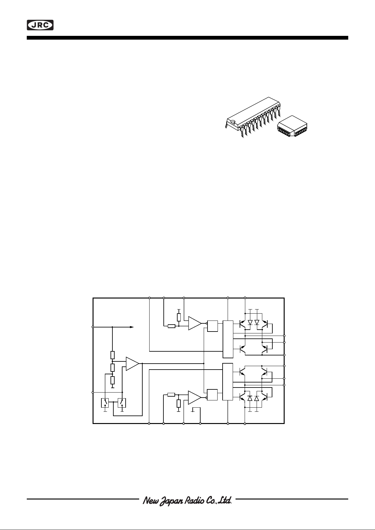
The NJM3772 is a stepper motor driver, which circuit is
especially developed for use in microstepping applications in
conjunction with the matching dual DAC (Digital-to-Analog
Converter) NJU39610.
The NJM3772 contains a clock oscillator, which is common
for both driver channels, a set of comparators and flip-flops
implementing the switching control, and two H-bridges with
internal recirculation diodes. Voltage supply requirements are
+5 V for logic and +10 to +45V for the motor. Maximum output
current is 1000mA per channel.
■ FEATURES
• Dual chopper driver
• 1000mA continuous output current per channel
• Specially matched to the Dual DAC NJU39610
NJM3772D2
NJM3772
NJM3772FM2
• Packages DIP22 / PLCC28
■ BLOCK DIAGRAM
NJM 3772
V
CC
RC
V
Phase
1
V
CC
+
—
C
R1
1
—
+
+
—
R
S
SRQ
Q
Logic
Logic
E
V
MM1
1
M
A1
M
B1
V
BB1
V
BB2
M
B2
M
A2
Figure 1. Block diagram
Phase
E
V
2
R2
GNDC
2
V
MM2
2
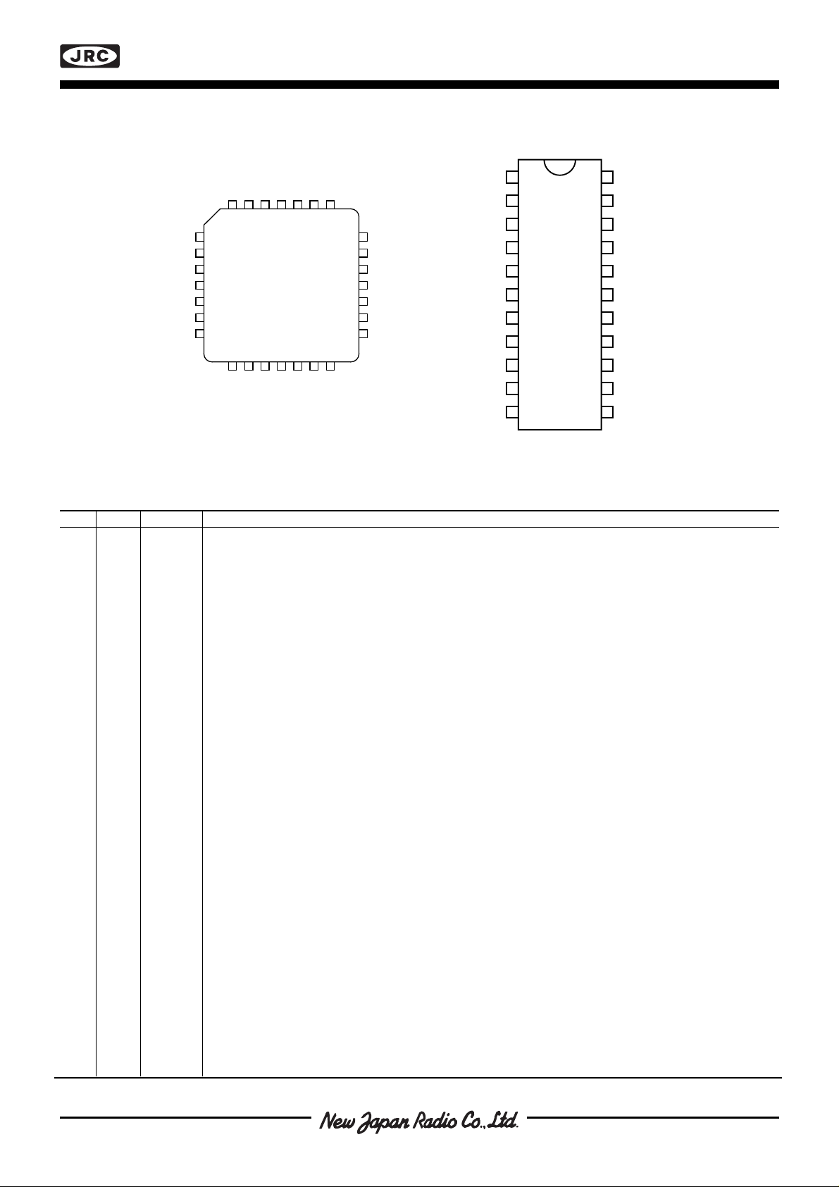
■ PIN CONFIGURATIONS
NJM3772
V
BB2
M
M
GND
V
BB1
A2
M
GND
4
3
5
E
6
2
7
B2
8
B1
NJM3772FM2
9
E
10
1
11
12131415161718
A1
M
GND
GND
2
GND
GND
1
GND
MM2
GND
V
282726
GND
GND
2
Phase
MM1
V
25
V
R2
24
C
2
23
RC
22
V
CC
21
C
1
20
V
R1
19
Phase
1
Phase
V
GND
GND
V
MM2
M
V
BB2
M
RC
C
R2
A2
E
B2
2
2
2
1
2
3
4
5
6
7
8
9
10
11
NJM
3772D2
22
21
20
19
18
17
16
15
14
13
12
V
CC
C
1
V
R1
Phase
GND
GND
V
MM1
M
A1
V
BB1
E
1
M
B1
1
Figure 2. Pin configurations
■ PIN DESCRIPTION
PLCC DIP Symbol Description
1-3, 9, 5, 6 GND Ground and negative supply. Note: these pins are used thermally for heat-sinking.
13-17 17, 18 Make sure that all ground pins are soldered onto a suitably large copper ground
28 plane for efficient heat sinking.
48M
59V
610E
711M
812M
10 13 E
11 14 V
12 15 M
18 16 V
A2
BB2
2
B2
B1
1
BB1
A1
MM1
19 19 Phase
20 20 V
21 21 C
22 22 V
R1
1
CC
23 1 RC Clock oscillator RC pin. Connect a 15 kohm resistor to V
24 2 C
25 3 V
2
R2
26 4 Phase
27 7 V
MM2
Motor output A, channel 2. Motor current flows from MA2 to MB2 when Phase2 is HIGH.
Collector of upper output transistor, channel 2. For lowest possible power dissipation, connect a
series resistor R
B2
to V
. See Applications information, External components.
MM2
Common emitter, channel 2. This pin connects to a sensing resistor RS to ground.
Motor output B, channel 2. Motor current flows from MA2 to MB2 when Phase2 is HIGH.
Motor output B, channel 1. Motor current flows from MA1 to MB1 when Phase1 is HIGH.
Common emitter, channel 1. This pin connects to a sensing resistor RS to ground.
Collector of upper output transistor, channel 1. For lowest possible power dissipation, connect a
series resistor R
B1
to V
. See Applications information, External components.
MM1
Motor output A, channel 1. Motor current flows from MA1 to MB1 when Phase1 is HIGH.
Motor supply voltage, channel 1, +10 to +40 V. V
Controls the direction of motor current at outputs MA1 and MB1. Motor current flows from MA1 to M
1
MM1
and V
should be connected together.
MM2
when Phase1 is HIGH.
Reference voltage, channel 1. Controls the threshold voltage for the comparator and hence the
output current.
Comparator input channel 1. This input senses the instantaneous voltage across the sensing
resistor, filtered by an RC network. The threshold voltage for the comparator is V
i.e. 450 mV at V
= 2.5 V.
R1
Logic voltage supply, nominally +5 V.
and a 3300 pF capacitor to ground to
CC
obtain the nominal switching frequency of 26.5 kHz.
Comparator input channel 2. This input senses the instantaneous voltage across the sensing
resistor, filtered by an RC network. The threshold voltage for the comparator is V
i.e. 450 mV at V
= 2.5 V.
R2
Reference voltage, channel 2. Controls the threshold voltage for the comparator and hence the
output current.
Controls the direction of motor current at outputs MA2 and MB2. Motor current flows from MA2 to M
2
when Phase2 is HIGH.
Motor supply voltage, channel 2, +10 to +40 V.V
MM1
and V
should be connected together.
MM2
= 0.18 • VR1 [V],
CH1
= 0.18 • VR2 [V],
CH2
B1
B2
NJM3772
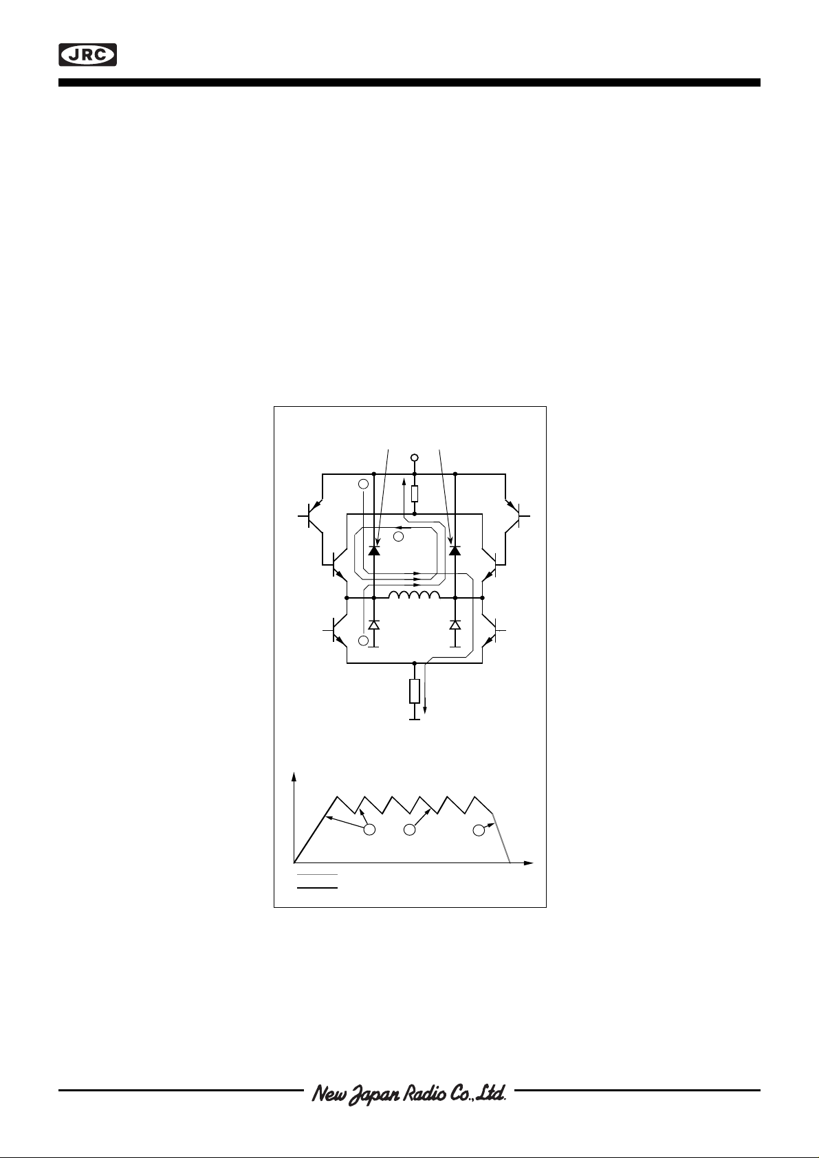
■ FUNCTIONAL DESCRIPTION
Each channel of the NJM3772 consists of the following sections: an output H-bridge with four transistors, capable
of driving up to 1000 mA continuous current to the motor winding; a logic section that controls the output transistors; an S-R flip-flop; and a comparator. The clock-oscillator is common to both channels.
Constant current control is achieved by switching the output current to the windings. This is done by sensing the
peak current through the winding via a current-sensing resistor RS, effectively connected in series with the motor
winding during the turn-on period. As the current increases, a voltage develops across the sensing resistor, which
is fed back to the comparator. At the predetermined level, defined by the voltage at the reference input VR, the
comparator resets the flip-flop, which turns off the output transistors. The current decreases until the clock oscillator
triggers the flip-flop, which turns on the output transistors again, and the cycle is repeated.
The current paths during turn-on, turn-off and phase shift are shown in figure 3. Note that the upper recirculation
diodes are connected to the circuit externally.
External recirculation diodes
V
MM
1
R
B
V
BB
2
3
R
S
Motor Current
1 2
Fast Current Decay
Slow Current Decay
3
Time
Figure 3. Output stage with current paths
during turn-on, turn-off and phase shift.
 Loading...