

JRC NJM3771D2, NJM3771FM2, NJM3771E3 Datasheet
DUAL STEPPER MOTOR DRIVER
■ GENERAL DESCRIPTION ■ PACKAGE OUTLINE
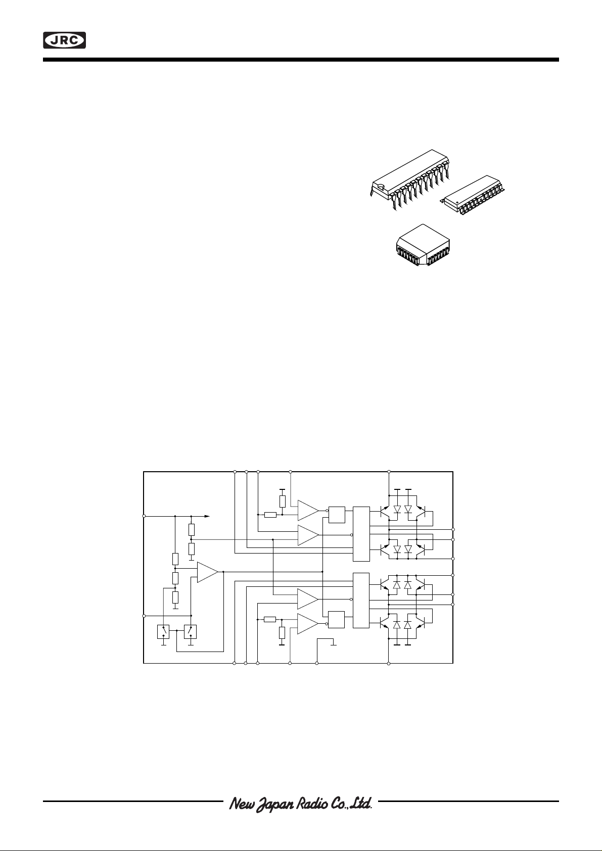
The NJM3771 is a stepper motor driver, which circuit is
especially developed for use in microstepping applications in
conjunction with the matching dual DAC (Digital-to-Analog
Converter) NJU39610.
The NJM3771 contains a clock oscillator, which is common
for both driver channels; a set of comparators and flip-flops
imple menting the switching control; and two H-bridges with
internal recirculation diodes. Voltage supply requirements are
+5 V for logic and +10 to +45 V for the motor. Maximum
output current is 650 mA per channel.
NJM3771D2
NJM3771
NJM3771E3
■ FEATURES
• Dual chopper driver
• 650 mA output current per channel
• Selectable slow/fast current decay for improved high-
speed microstepping
• Specially matched to Dual DAC NJU39610
• Packages DIP22 / EMP24(Batwing) / PLCC28
■ BLOCK DIAGRAM
VR1CD
1
1
V
CC
RC
NJM3771
Phase
V
CC
+
–
NJM3771FM2
C
1
–
+
+
–
–
+
+
–
R
S
SRQ
Q
Logic
Logic
E
1
M
A1
M
B1
V
MM1
V
MM2
M
B2
M
A2
Figure 1. Block diagram
Phase
VR2CD
2
2
GNDC
2
E
2
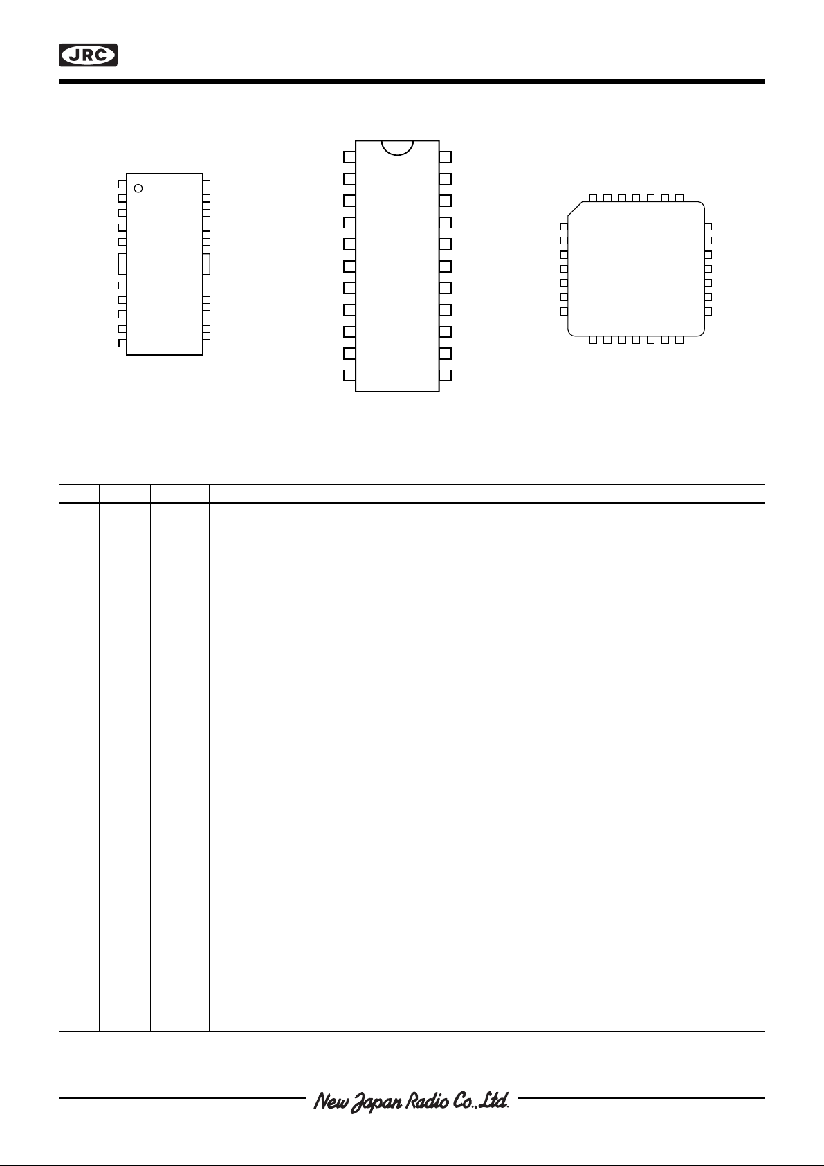
■ PIN CONFIGURATIONS
1
2
3
4
5
6
8
9
10
11
22
21
20
19
18
17
16
15
14
1312
GND
MA
1
MA
2
GND
NC
NJM
3771E3
MB
1
E
1
VMM
1
NC
MB
2
E
2
VMM
2
VR
2
CD
2
C
2
RC
23
24
GND
GND
Phase
2
7
VR
1
CD
1
C
1
V
CC
Phase
1
NJM3771
M
V
MM1
M
GND
GND
Phase
CD
V
V
E
C
CC
B1
A1
R1
1
1
1
1
1
2
3
4
5
6
7
8
9
10
11
NJM
3771D2
22
21
20
19
18
17
16
15
14
13
12
M
B2
E
2
V
MM2
M
A2
GND
GND
Phase
CD
2
V
R2
C
2
RC
2
A2
M
GND
GND
GND
GND
GND
1
GND
432
5
V
MM2
E
6
2
M
7
B2
M
8
B1
NJM 3771FM2
GND
2
9
10
E
1
V
11
MM1
12131415161718
A1
M
GND
Phase
282726
GND
GND
2
CD
1
Phase
25
V
R2
C
24
2
RC
23
V
22
CC
C
21
1
20
V
R1
19
CD
1
Figure 2. Pin configurations
■ PIN DESCRIPTION
Refer to Figure 2
EMP DIP PLCC Symbol Description
218MB1Motor output B, channel 1. Motor current flows from MA1 to MB1 when Phase1 is HIGH.
3210E
4311V
5412MA1Motor output A, channel 1. Motor current flows from MA1 to MB1 when Phase1 is HIGH.
6,7, 5,6, 1-3,9, GND Ground and negative supply. Note: these pins are used thermally for heat-sinking.
18,19 17,18 13-17,28 Make sure that all ground pins are soldered onto a suitably large copper ground
8 7 18 Phase
9819CD
10 9 20 V
11 10 21 C
12 11 22 V
13 12 23 RC Clock oscillator RC pin. Connect a 15 kohm resistor to VCC and a 3300 pF capacitor to
14 13 24 C
15 14 25 V
16 15 26 CD2Current decay control, channel 2. A logic HIGH on this input results in
17 16 27 Phase
20 19 4 M
21 20 5 V
22 21 6 E
23 22 7 M
Common emitter, channel 1. This pin connects to a sensing resistor to ground.
1
Motor supply voltage, channel 1, 10 to 40 V. V
MM1
MM1
and V
should be connected together.
MM2
plane for efficient heat sinking.
Controls the direction of motor current at outputs MA1 and MB1. Motor current flows from M
1
to MB1 when Phase1 is HIGH.
Current decay control, channel 1. A logic HIGH on this input results in
1
a LOW results in
Reference voltage, channel 1. Controls the threshold voltage for the comparator and hence
R1
fast
current decay, see “Functional Description.”
slow
current decay,
the output current. Input resistance is typically 2.5 kohms, ±20%.
Comparator input channel 1. This input senses the instantaneous voltage across the
1
sensing resistor, filtered by an RC network. The threshold voltage for the comparator is
(0.450 / 2.5) • VR1, i.e. 450 mV at VR1 = 2.5 V.
Logic voltage supply, nominally +5 V.
CC
ground to obtain the nominal switching frequency of 26.5 kHz.
Comparator input channel 2. This input senses the instantaneous voltage across the
2
sensing resistor, filtered by an RC network. The threshold voltage for the comparator is
(0.450 / 2.5) • VR1, i.e. 450 mV at VR1 = 2.5 V.
Reference voltage, channel 2. Controls the threshold voltage for the comparator and hence
R2
the output current. Input resistance is typically 2.5 kohms, ±20%.
slow
current decay,
a LOW results in
Controls the direction of motor current at outputs MA2 and MB2. Motor current flows from M
2
fast
current decay, see “Functional Description.”
to MB2 when Phase2 is HIGH.
Motor output A, channel 2. Motor current flows from MA2 to MB2 when Phase2 is HIGH.
A2
Motor supply voltage, channel 2, 10 to 40 V. V
MM2
Common emitter, channel 2. This pin connects to a sensing resistor to ground.
2
Motor output B, channel 2. Motor current flows from MA2 to MB2 when Phase2 is HIGH.
B2
MM1
and V
should be connected together.
MM2
A1
A2
NJM3771
■ FUNCTIONAL DESCRIPTION
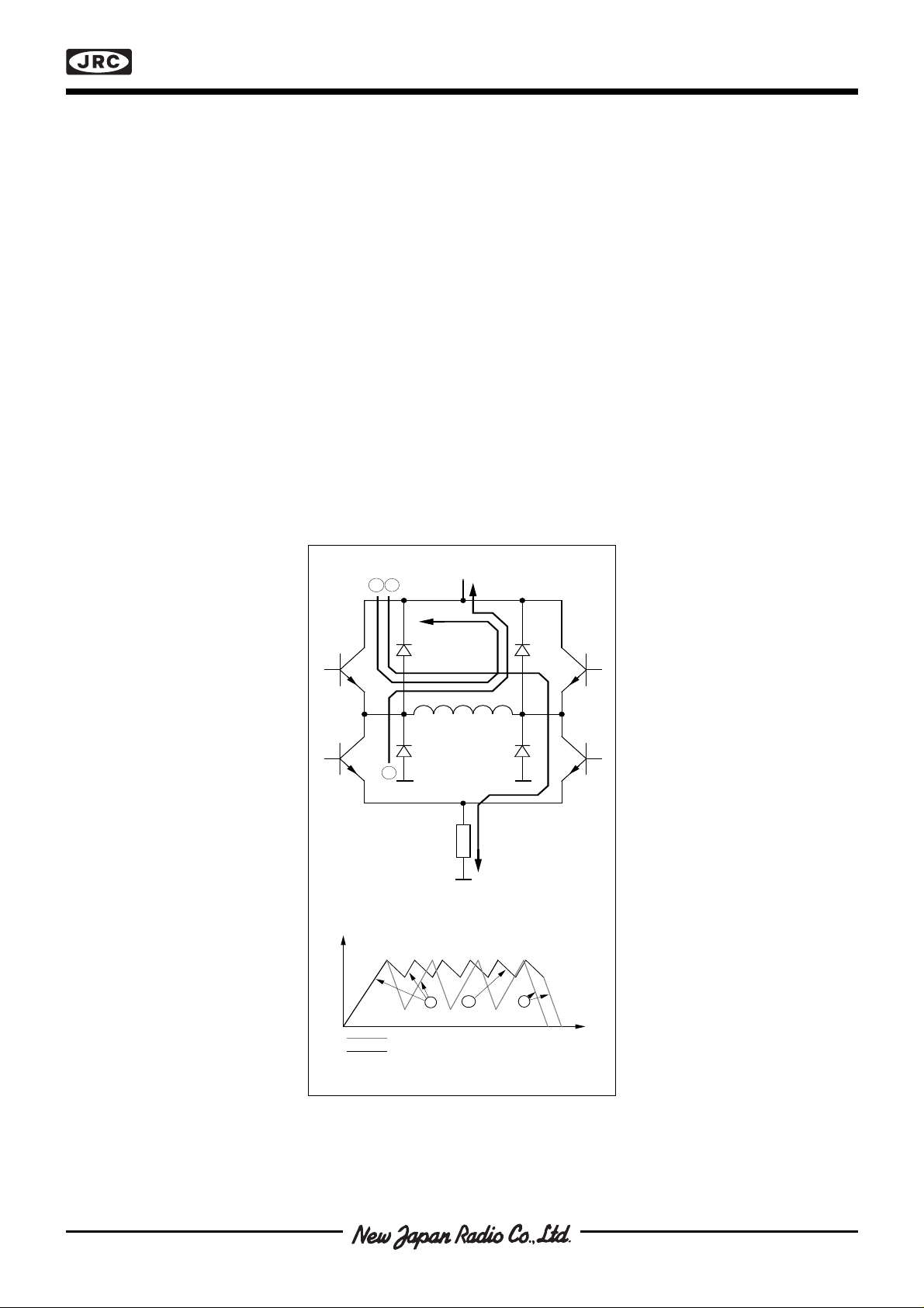
Each channel of the NJM3771 consists of the following sections: an H-bridge output stage, capable of driving up
to 650 mA continuous motor current (or 500 mA, both channels driven), a logic section that controls the output
transistors, an S-R flip-flop, and two comparators. The oscillator is common to both channels.
Constant current control is achieved by switching the current to the windings. This is done by sensing the (peak)
voltage across a current-sensing resistor, RS, effectively connected in series with the motor winding, and feeding
that voltage back to a comparator. When the motor current reaches a threshold level, determined by the voltage at
the reference input, VR, the comparator resets the flip-flop, which turns off the output transistors. The current
decreases until the clock oscillator triggers the flip-flop, which turns on the output transistors again, and the cycle is
repeated.
The current-decay rate during the turn-off portion of the switching cycle, can be selected fast or slow by the CD
input.
In slow current-decay mode, only one of the lower transistors in the H-bridge (those closest to the negative
supply) is switched on and off, while one of the upper transistors is held constantly on. During turn-off, the current
recirculates through the upper transistor (which one depends on current direction) and the corresponding freewheeling diode connected to VMM, see figure 3.
In fast current decay mode, both the upper and lower transistors are switched. During the off-time, the freewheeling current is opposed by the supply voltage, causing a rapid discharge of energy in the winding.
Fast current decay may be required in half- and microstepping applications when rapid changes of motor current
are necessary. Slow current decay, however, gives less current ripple, and should always be selected, if possible,
to minimize core losses and switching noise.
Motor Current
1
2
3
R
s
1
32
FAST Current Decay
SLOW Current Decay
Time
Figure 3. Output stage with current paths
during turn -on, turn-off and phase shift
 Loading...