

JRC NJM3545TA2 Datasheet
UNIVERSAL SINK DRIVER
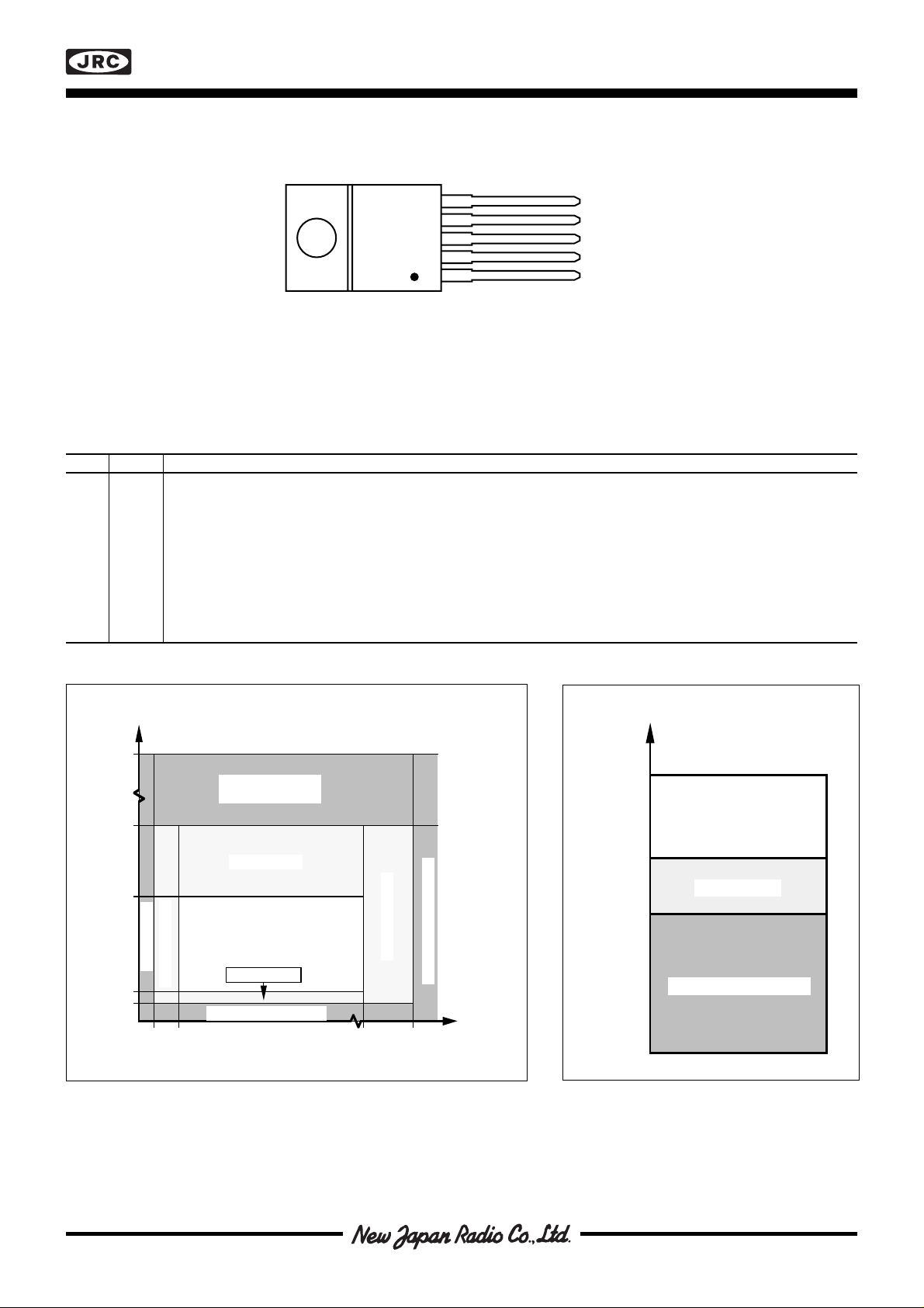
■ GENERAL DESCRIPTION ■ PACKAGE OUTLINE
NJM3545 is a bipolar universal high-current highly protected
low side driver with transparent input and 2000mA continuous
-current sink capability. A high-level input activates the output.
The driver is equipped with extensive electrical protection;
such as over current protection and thermal protection,
which makes the device virtually indestructible.
Furthermore it can detect open circuit and short circuit to ground.
A special feature is the Error indicating output function pin
which signals to the host system if the protection or the load
check functions is activated.
The NJM3545 and NJM3548 are complementary drivers and
have similar data.
■ FEATURES
• 2000mA continuous-output current
NJM3545TA2
NJM3545
• Short circuit to VCC protection
• Error signal to host system
• Open circuit detection
• Short circuit to ground detection
• Thermal protection
• Built-in protection diodes
• Package TO-220 (5-pin)
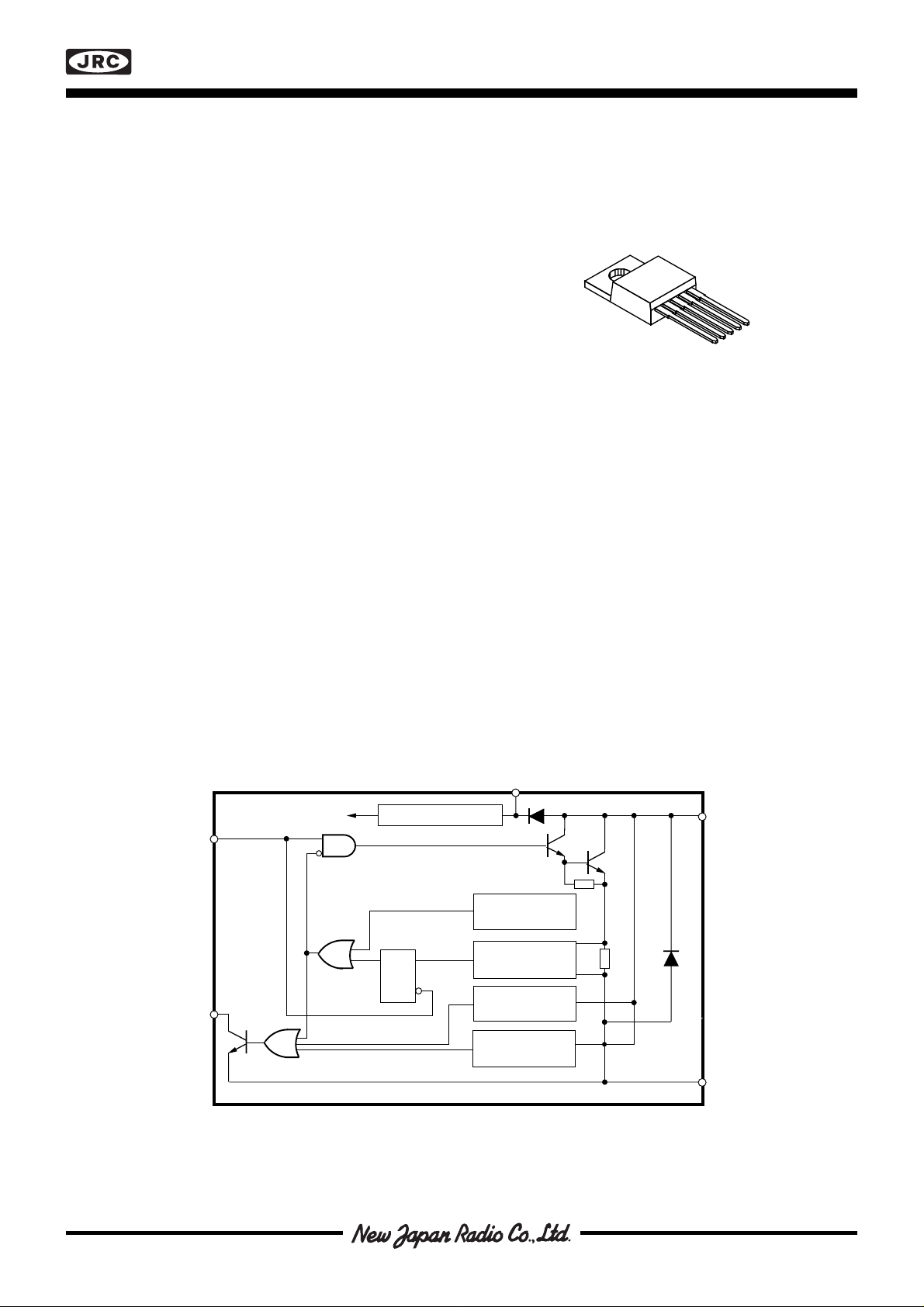
■ BLOCK DIAGRAM
NJM3545
Input
Error
To logic
Voltage reference
QRS
Open circuit
detection
Supply
Thermal
protection
Short-circuit to
V protection
cc
Short-circuit to
GND detection
Output
Figure 1. Block Diagram
GND
■ PIN CONFIGURATION
NJM3545
NJM3545TA2
5
4
3
2
1
Input
Error
GND
Output
Supply
Figure 2. Pin description
■ PIN DESCRIPTION
TO-220 Symbol Description
1 Supply Supply voltage. Nominally 5 V to 40 V.
2 Output Output pin. Current flows from supply through the load into the pin. Nominal current is 8 mA to 2 A.
3 GND Ground supply.
diode are bonded to a separate pin.
4 Error Error indicating pin. Sinks current to ground if the protection and/or detection circuitry is activated.
Note: the current must be externally limited to 8 mA.
5 Input TTL compatible input. A LOW input signal turns the output transistor off and a HIGH input turns it on.
Output
voltage
V
cc
3.5 V
2.1 V
Open circuit
0.6 V
0.2 V
(min 0.5 mA, max 8 mA)
Undefined area
I
OMIN
Short circuit to GND error
NJM3545
Active output
Overload or short
circuit to V Error
cc
Undefined area
Normal operation
Undefined area
Undefined area
Short circuit protection
I
OS
(min 2 A, max 4.5 A)
Output
current
Figure 3. Error state vs. output voltage and output current, active
output (2.0 ≤ VIN ≤ VCC), 5 V < VCC < 40 V, - 40°C <TJ < +100°C
Output
voltage
NJM3545
Inactive output
100% V
cc
Normal operation
70% V
cc
Undefined area
50% V
cc
Short circuit to GND Error
0% V
cc
Figure 4. Error state vs. output voltage,
inactive output (0 V ≤ VIN ≤ 0.8 V), 5 V ≤
VCC ≤ 40 V, - 40°C < TJ < +100°C
NJM3545
■ FUNCTIONAL DESCRIPTION
The circuit NJM3545 is a low side driver capable of driving resistive or inductive loads not exceeding 2 A.
The driver has an error indicating function which generates an Error output signal when a fault condition has
occurred.
The circuits NJM3545 and NJM3548 are complementary drivers with equivalent functions and similar data.
NJM3545 is a sink driver and NJM3548 is a source driver.
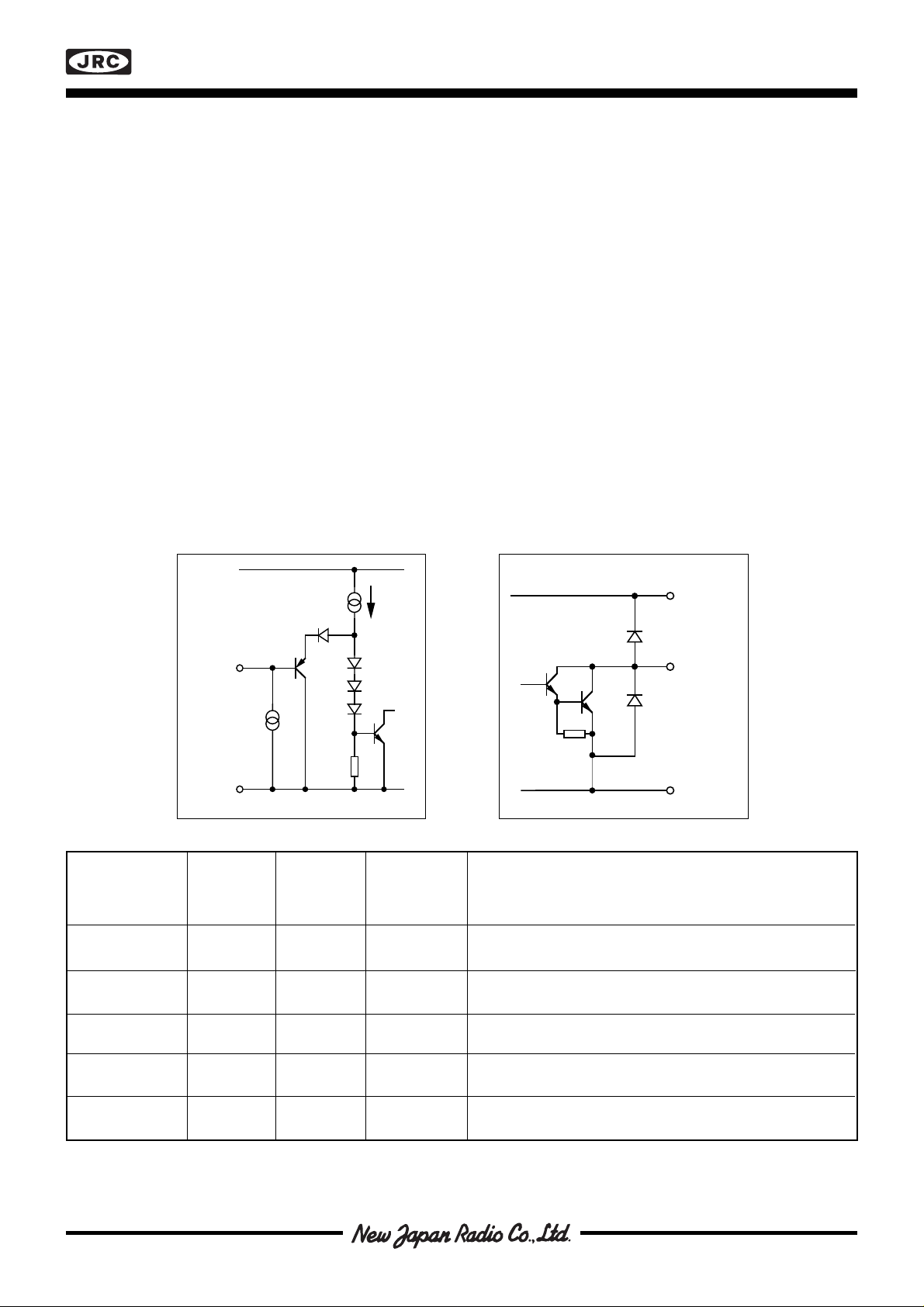
Input stage
The output stage is switched on and off according to the status of the input. HIGH level activates the output. If the
input is left open, the circuit will accept it as a LOW level.
Output stage
The output stage contains a power transistor and two clamping diodes. The diodes are used for terminating line
transients from inductive loads. If the driver is inactive and the output is shorted to GND the driver will leak maximum
8 µA. See figure 18.
Protection circuit
The circuit contains two protection circuits:
• Overload and Short circuit protection
• Thermal protection
The overload and short circuit protection will be activated at I
The output will be turned off immediately and latched to a high-impedance state after an overload or short circuit
has been detected.
= 3.5 A typically at TJ= +25°C, see figure 20.
out
1
Input
I
Ref
5
CC
2
Output
3
GND
3
Figure 6. Output stageFigure 5. Input stage
Fault condition Input Output Error How to resume normal operation
LOW=Error
HIGH=Normal
Normal 0 LOW 1 OFF 1 HIGH ——
1 HIGH 0 ON 1 HIGH ——
V
Short to GND 0 LOW 1 OFF 0 LOW Remove fault condition.
OUT
1 HIGH 0 ON 0 LOW Remove fault condition.
V
Short to V
OUT
Open load 0 LOW 1 OFF 1 HIGH ——
Over temperature 0 LOW 1 OFF 1 HIGH ——
=130 °C 1 HIGH 1 OFF 0 LOW Temperature is reduced to approx 120°C, or turn off the driver.
T
J
Figure 7. Error table
0 LOW 1 OFF 1 HIGH ——
CC
1 HIGH 1 OFF 0 LOW Turn off and on after fault condition is removed.
1 HIGH 0 ON 0 LOW Attach proper load to output or turn off the driver.
GND
 Loading...