

JRC NJM2370R, NJM2370U Datasheet
NJM2370
LOW DROPOUT VOLTAGE REGULATOR WITH ON/OFF CONTROL
■ GENERAL DESCRIPTION ■ PACKAGE OUTLINE
The NJM2370 is a low dropout voltage regulator with
ON/OFF control.
It features dropout voltage of 0.1V at Io=30mA, low
output noise and high ripple rejection by connecting an
external capaciter to noise bypass terminal.
It’s suitable for portable items such as cellular phones,
video camera and others.
■ FEATURES
● Output Current (150mA min. (Vo-0.3V))
● Low Dropout Volt age (0.1V typ. (Io=30mA))
● External Capaciter for Noise Bypass
● ON/OFF Control Function
● Over Current Limit
● Thermal Shutdown
● Bipolar Technology
● Package Outline SOT-89(5pin), VSP8
■ PIN CONFIGURATION
NJM2370U NJM2370R
5 4
1 2 3
PIN FUNCTION
CONTROL
1.
GND
2.
NOISE BYPASS
3.
V
OUT
VIN
4.
5.
1
2
3
4
NJM2370U NJM2370R
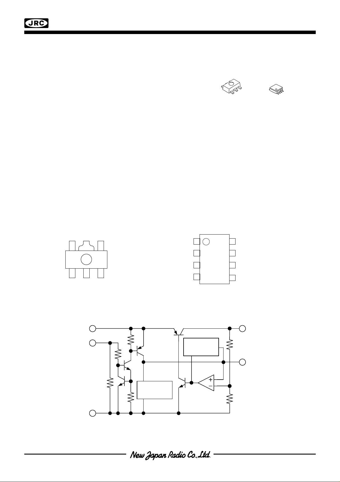
■ EQUIVALENT CIRCUIT
VIN
CONT
Bandgap
Reference
Thermal
Protection
PIN FUNCTION
8
1. CONTROL
2. GND
7
3. NC
4. NOISE BYPASS
6
5. V
OUT
6. NC
5
7. NC
8. V
IN
V
OUT
NOISE
BYPASS
GND
- 1/1 -
NJM2370_databook00_01
NJM2370
■ ABSOLUTE MAXIMUM RATINGS (Ta=25°C)
PARAMETER SYMBOL RATINGS UNIT
Input Voltage VIN 20 V
Control Vo lt age V
Power Dissipation PD
Operating Temperature Range
Storage Temperature Range
(note 1)When input voltage is less than +20V, the absolute maximum
control voltage is equal to the input vo lt age.
■ ELECTRICAL CHARACTERISTICS (Ta=25°C)
PARAMETER SYMBOL CONDITIONS MIN. TYP. MAX. UNIT
Output Voltage Vo
Quiescent Current 1 IQ1 Io=0mA,expect I
Quiescent Current 2 IQ2
Output Current Io
Line Regulation
Load Regulation
Dropout Voltage
Ripple Rejection
Average Temperature
∆Vo/∆V
∆Vo/∆Io Io=0 ∼ 60mA
∆V
I-O
R • R
∆Vo/∆Ta Ta=−20 ∼ 75°C, Io=10mA
Coefficient of Output
Voltage
Output Noise Voltage VNO 10Hz< f < 80kHz, Io=10mA, Vo=3V
(note 2)Please confirm the specification separately because some parameters depend on output voltage.
■ TEST CIRCUIT
20(note 1) V
CONT
Topr
Tstg
(SOT-89)
(VSP8)
−40 ∼ +85 °C
−40 ∼ +125 °C
V
=Vo+ 1V, Io=30mA
IN
350
320
CONT
CONTROL−GND short
(Vo−0.3V)
VIN=(Vo+1V) ∼ (Vo+6V)
IN
Vo=2V to 14V
V
=(Vo+1V) ∼ (Vo+5V)
IN
Vo=15V
Io=30mA
f=400Hz, ein=100mVp-p
=Vo+ 1. 5V, Io=10mA
V
IN
=Vo+1.5V
V
IN
mW
−3%
−
−
180
− −
150 180
− −
− −
− −
−
−
−
−
0.1 0.3 V
60
0. 2
30
+3% V
−
µA
100 nA
−
mA
0.12 %/V
0.12 %/V
0.03 %/mA
−
−
−
dB
mV/°C
µVrms
V
IIN
A
+
IN
V
V
A
CONT
0.1µF
I
CONT
VIN V
NJM2370
CONTROL
NOISE
BYPASS
GND
OUT
+
I
10µF
V
OUT
V
OUT
Cp
-
-
2/2
NJM2370_databook00_01
R
NJM2370
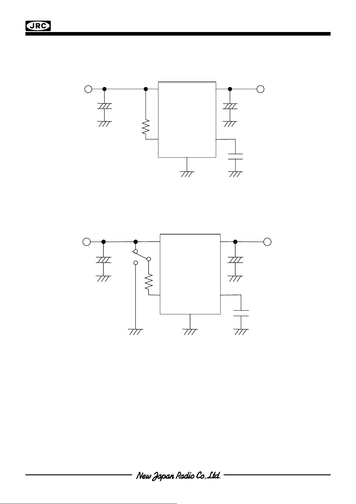
■ TYPICAL APPLICATION
In Nonuse of ON/OFF Control
①
V
IN
+
0.1µF
(0~300kΩ)
Connect control terminal(1Pin) to V
terminal(5Pin)
IN
When a resistance “R” is connected, the quiescent current decreases, but minimum operating voltage
increases. Please refer to a figure of Output V olt age vs. Control Voltage.
In Use of ON/OFF CONTROL
②
VIN V
OUT
NJM2370
CONTROL
NOISE
BYPASS
GND
+
10µF
Cp=0.1µF
V
OUT
V
IN
+
0.1µF
VIN V
NJM2370
OUT
+
10µF
V
OUT
R
GND
NOISE
BYPASS
Cp=0.1µF
CONTROL
When the control terminal is “H”, it is ON.
When the control terminal is “L” or “open”, it is OFF.
✱Noise bypass Capacitance Cp
Noise bypass capacitance CP reduces noise generated by band-gap reference circuit.
Noise level and ripple rejection will be improved when larger CP is used. Please refer to the typical
characteristics to determine the value.
Use of smaller CP value may induce oscillation.
Please make sure to use CP value of greater than 0.1uF to avoid the problem.
-
-
3/3
NJM2370_databook00_01
 Loading...