

JRC NJM2367TLA2050, NJM2367TA2050 Datasheet
r
y
w
NJM2367
5.5A HIGH POWER DC/DC CONVERTER CONTROLLER IC
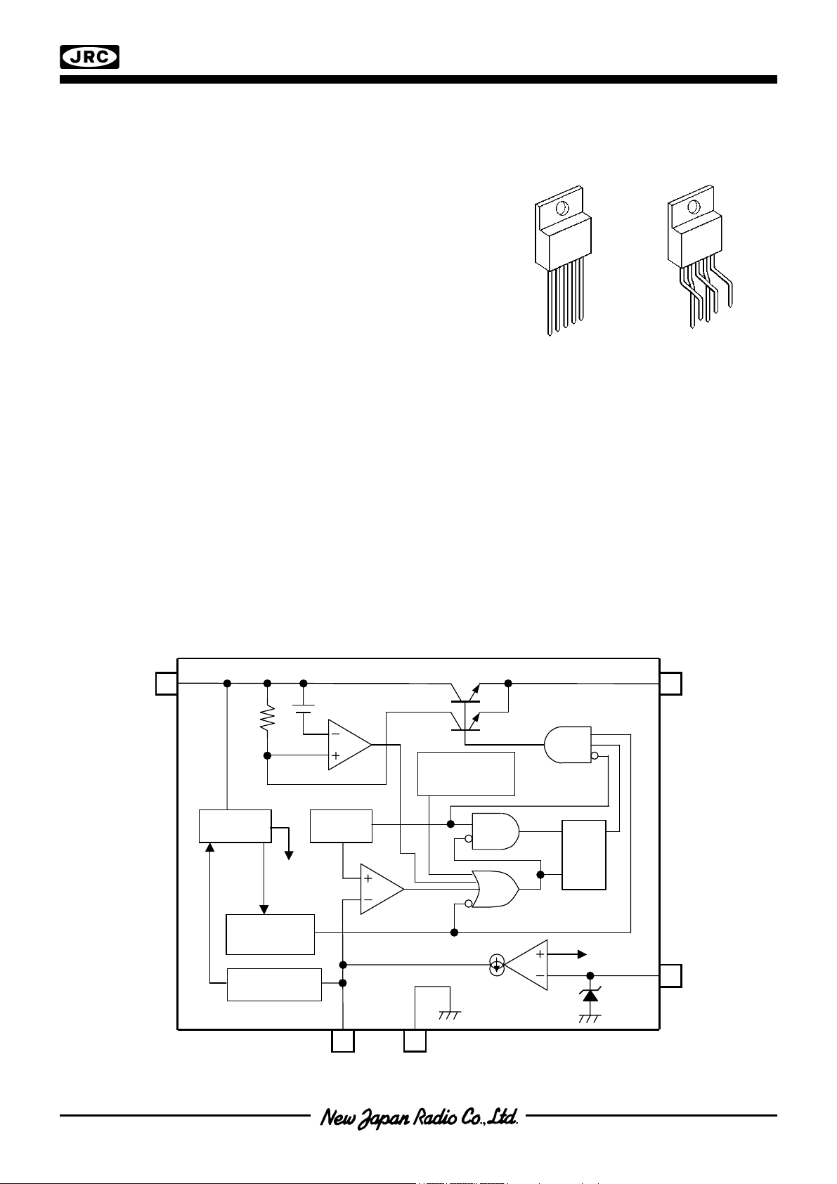
■GENERAL DESCRIPTION ■PACKAGE OUTLINE
NJM2367
The
inducing basic function of DC/DC converter controller, which
consists precision reference voltage, fixed frequenc
oscillator, high gain error amplifier, precision output switch,
cycle-by-cycle current limit, under voltage lockout, and
thermal shutdown circuit.
NJM2367
The
external parts, and realize low power stand-by mode.
■FEATURES
●Operating Voltage (7.5V to 40V)
●PWM form Switching Power Supply Control
●Internal High Power Transistor 5.5A (min.)
●Fixed Frequency Oscillator 72kHz (typ.)
●Internal Current Sense Amplifier
●Internal Under Voltage Lockout
●Internal Thermal Shutdown Circuit
●Bipolar Technology
●Package Outline TO-22O(5PIN)
■BLOCK DIAGRAM
is a high power DC/DC converter controlle
is suitable for step-down converter with fe
1 2 3 4 5
NJM2367TA2050 NJM2367TLA2050
PIN FUNCTION
1:V
FB
2:SW
OUT
3:GND
+
4:V
5:STBY (V
COMP
)
4
Reference
Voltage
ON/OFF
Under Voltage
Lockout
Standby Circuit
VREF
Current Sense
Amplifier
Oscillator
PWM Comparator
5.5A Power Transistor
Current Circh Transistor
Thermal
Shutdown
Ratch Circuit
Error Amplifier
S
R
2
Q
VREF
1
5
3
- 1 -
Ver 2.1
NJM2367
■ABSOLUTE MAXIMUM RATINGS (Ta=25°C )
PARAMETER SYMBOL RATINGS UNIT
Maximum Supply Voltage V+ 40 V
Switch Output Voltage Vo
Voltage Feedback and
Compensation Input Voltage Range
(SWITCH)
V
FB,VCOMP
Power Dissipation
Operating Junction Temperature
Operating Temperature Range
Storage Temperature Range
Topr
Ts tg
■THERMAL CHARACTERISTICS
Thermal
Resistance
Junction-to-Ambient Temperature θja 70
Junction-to-Case θjc 6.5
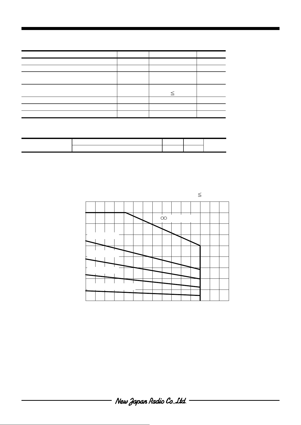
■POWER DISSIPATION vs. AMBIENT TEMPERATURE
P
Tj
-0.5 ∼ +Vin
-0.3 ∼ +7.0
D
TO-220 (5PIN)
16(T
46°C)
C
-40 ∼ +150
-40 ∼ +85
-50 ∼ +150
V
V
W
°C
°C
°C
°C/W
(T
=-40~+85°C, Tj= ~+150°C, PD=16W(T
opr
18
16
Heat Sink
14
(W)
D
12
θHS=5°C/W
10
θHS=10°C/W
8
6
θHS=20°C/W
4
Power Dissipation P
Without Heat Sink
2
0
25 50 75 100
Ambient Temperature Ta (°C)
C
46°C))
- 2 -
NJM2367
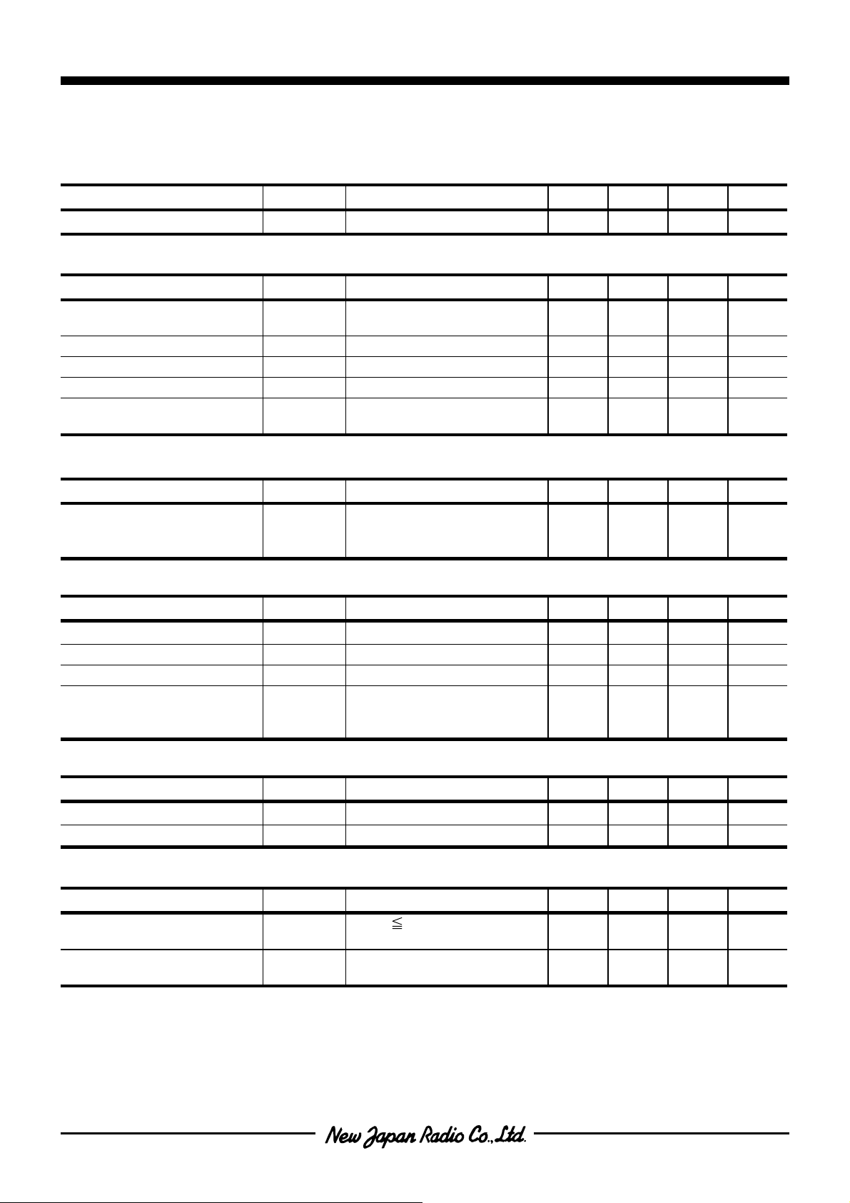
■ELECTRICAL CHARACTERISTICS (V
+
=12V, Ta=25°C)
OSCILLATOR BLOCK
PARAMETER SYMBOL TEST CONDITIONS MIN. TYP. MAX. UNIT
Frequency fosc V+=7.5V 65 72 79 kHz
ERROR AMPLIFIER BLOCK
PARAMETER SYMBOL TEST CONDITIONS MIN. TYP. MAX. UNIT
Voltage Feedback
VFB(th) 4.9 5.0 5.1 V
Input Threshold
Line Regulation REG·Line
+
V
=7.5 ∼ 40V
– 0.03 0.08 %/V
Input Bias Current IB VFB=VFB(th)+0.15V – 0.15 1.0 μA
Ripple Rejection PSRR
Output Voltage Swing VOH
V
OL
+
V
=10 ∼ 20V
Isource=75μA,V
Isink=0.4mA,V
FB
=5.3V
FB
=4.7V
– 80 – dB
4.2
–
4.9
1.6
–
1.9
V
V
PWM COMPARATOR BLOCK
PARAMETER SYMBOL TEST CONDITIONS MIN. TYP. MAX. UNIT
Duty Cycle
Maximum
Minimum
DC
DC
(MAX)
(MIN)
V
=0V
FB
V
=5.3V
FB
–
0
95
0
–
0
%
%
SWITCH OUTPUT BLOCK
PARAMETER SYMBOL TEST CONDITIONS MIN. TYP. MAX. UNIT
Output Voltage Saturation V
OFF-State Leakage Isw
Current Limit Threshold Ipk
Switching Times
Output Voltage Rise Time
Output Voltage Fall Time
V+=7.5V,Isource=5.5A – V+-1.5 V+-1.8 V
SAT
V+=40V,SW
(off)
(SWITCH)
V+=7.5V 5.5 6.5 8.0 A
tr
tf
V
V
+
=40V,R
+
=40V,R
=0V – 0 100 μA
OUT
=7.7Ω,VFB=0V
OUT
=7.7Ω,VFB=0V
OUT
–
–
100
50
UNDER VOLTAGE LOCKOUT BLOCK
PARAMETER SYMBOL TEST CONDITIONS MIN. TYP. MAX. UNIT
Startup Threshold V
Hysteresis V
TH(UVLO)
H(UVLO)
V+ Increasing 5.9 6.3 6.7 V
V+ Decreasing 0.6 0.8 1.0 V
TOTAL DEVICE
PARAMETER SYMBOL TEST CONDITIONS MIN. TYP. MAX. UNIT
Standby-State
Icc
STBY 0.1V – 36 100 μA
(stby)
Power Supply Current
Operating-State
Power Supply Current
Icc V+=40V,VFB=0V
duty·cycle=MAX
– 40 53 mA
Keep the limit of maximum power dissipation not to operate thermal shutdown.
Low duty cycle pulse test is used to close its junction temperature to ambient temperature.
–
–
nS
nS
- 3 -
 Loading...