

Page 1
PDA(N) Series - Sensor-Less Vector
PDH Series - High Frequency
PDE Serie - Wide Application
Inverter Instruction Manual
Version: 2.1
Page 2
1
WARNING!
Attention to these warning signs on the inverter or in this instruction book, they indicate danger to
human body or damage to the inverter.
Before installing and putting the inverter into operation, please read the safety precautions and warnings
following this page.
!
Safety precautions & warnings
Read carefully all the safety precautions included in these operating instructions and all the warning signs attached to the
inverter. Make sure that the warning signs are kept in a legible condition and replace missing or damaged signs.
Before starting, familiarize yourself with the operation of the inverter. It may be too late if you start working with the inverter
before read this instruction manual.
Never permit unqualified personnel to operate the inverter.
!
WARNING
This inverter produces dangerous electrical voltages and controls rotating mechanical parts. Death, severe injury or
substantial damage to property can occur if the instructions in this operating manual are not completed with.
Only personnel with appropriate qualifications should work with this inverter. These personnel must be familiar with all the
warning signs and precautions laid out in these operating instructions for the transport, installation and operation of this
inverter.
The successful and safe use of this inverter depends on the correct installation, commissioning, operation and maintenance of
the inverter.
This inverter operates at high voltages.
l The DC-link capacitors remain charged to dangerous voltages even the power is removed. For this reason it is not
permissible to open the inverter cover until five (5) minutes after the power has been turned off. When handling the
open inverter it should be noted that live parts are exposed. Do not touch these live parts.
l The terminals R, S, T, U, V, W, P, N, B, PR, BR can carry dangerous voltages even if the motor is inoperative:
l Only qualified personnel may connect, start the system up and repair faults. These personnel must be thoroughly
acquainted with all the warnings and operating procedures contained with this manual.
l Certain parameter settings may cause the inverter to start up automatically after power on or power recover.
DEFINITIONS
Qualified Person
For the purposes of this manual and product labels, a qualified person is one who is familiar with the installation, construction,
operation and maintenance of this inverter and with hazards involved. In addition, the person must be:
l Trained and authorized to energize, de-energize, clear, ground and tag circuits and equipment in accordance
with established safety practices.
l Trained in the proper care and use of protective equipment in accordance with established safety practices.
l Trained in rendering first aid.
Danger
For the purposes of this manual and product labels, DANGER indicates that loss of life, severe personal injury or substantial
property damage WILL result if proper precautions are not taken.
Warning
For the purposes of this manual and product labels, WARNING indicates that loss of life, severe personal injury or
substantial property damage CAN result if proper precautions are not taken.
Caution
For the purpose of this manual and product labels, CAUTION indicates that minor personal injury or property damage CAN
result if proper precautions are not taken.
Note
For the purpose of this manual and product labels, NOTES merely call attention to information that is especially significant in
understanding and operating the drive.
!
DANGER and WARNING
Make sure that the location selected for installation is safe, protected from moisture and splash and drip-proof!
Children and the general public must be prevented from accessing or approaching the equipment!
The equipment may only be used for the purpose specified by the manufacturer.
Unauthorized modifications and the use of spare parts and accessories that are not sold or recommended by the manufacturer
of the equipment can cause fires, electric shocks and injuries.
Keep these operating instructions within easy reach and give them to all users!
!
WARNING
This is a Class A product. In a domestic environment this product may cause radio interference in which case the
user may be required to take adequate measures.
Page 3

2
CONTENTS
1 Description of PDAN/PDA/PDH/PDE Series inverter....................................................................................................3
1.1 General description and Design philosophy.................................................................................................................3
1.2 Control input & output configuration...........................................................................................................................3
1.3 Electrical Specifications..............................................................................................................................................5
2 INSTALLATION............................................................................................................................................................6
2.1 Outline Dimensions....................................................................................................................................................6
2.2 Power Terminal..........................................................................................................................................................7
2.3 Connect Power line input to Inverter...........................................................................................................................7
2.4 Connect inverter output to Motor................................................................................................................................7
2.5 Control terminal connection........................................................................................................................................7
2.6 DC bus terminal (P, N) or Brake terminal (B, P)..........................................................................................................8
2.7 A.C.L.........................................................................................................................................................................8
3 CONTROL PANEL........................................................................................................................................................9
3.1 CTL mode..................................................................................................................................................................9
3.2 MON mode................................................................................................................................................................9
3.3 PAR mode..................................................................................................................................................................9
3.4 ALM mode.................................................................................................................................................................9
4 SYSTEM START-UP....................................................................................................................................................10
4.1 Reset & Initialize the inverter....................................................................................................................................10
4.2 Setup Basic Motor Parameter....................................................................................................................................10
4.3 PDA series Operation Mode Selection.......................................................................................................................10
4.4 Auto Tuning.............................................................................................................................................................11
4.5 Monitor Selection.....................................................................................................................................................13
4.6 Simple application example......................................................................................................................................13
5 PARAMETERS.............................................................................................................................................................14
5.1 Parameter List..........................................................................................................................................................14
5.2 Parameter Protection.................................................................................................................................................16
5.3 Parameter Initialization.............................................................................................................................................16
5.4 Description of All Parameters...................................................................................................................................17
6. Selection of RUN/STOP/FWD/REV control command...............................................................................................23
7. Selection of Set Frequency............................................................................................................................................24
7.1 Set Frequency Source Selection Table.......................................................................................................................24
7.2 Description of Frequency Input Sources....................................................................................................................25
8. Selection of Digital input function................................................................................................................................32
9. Selection of Digital output and Relay function.............................................................................................................39
10. Selection of Analog output function...........................................................................................................................44
11. Speed search and Base Block function.......................................................................................................................45
12. AUTO RUN Function.................................................................................................................................................46
12.1 Auto Mode Selection & Running.............................................................................................................................46
12.2 Auto Run Status Output..........................................................................................................................................48
13. MONITOR function...................................................................................................................................................49
13.1 Operating Status Check...........................................................................................................................................49
13.2 Terminal Status Check............................................................................................................................................49
13.3 A/D Converter Check..............................................................................................................................................50
14. MAINTENANCE & ERROR MESSAGE.................................................................................................................51
15. RS485 Communication...............................................................................................................................................52
15.1 RS485 Communication port related parameter.........................................................................................................52
15.2 RS485 Configuration..............................................................................................................................................52
15.3 JPS Protocol & Format............................................................................................................................................53
15.4 Modbus Protocol.....................................................................................................................................................54
16. BLOCK DIAGRAM OF PDA INVERTER...............................................................................................................55
Appendix A:PID Function.............................................................................................................................................56
Page 4
3
1 Description of PDAN/PDA/PDH/PDE Series inverter
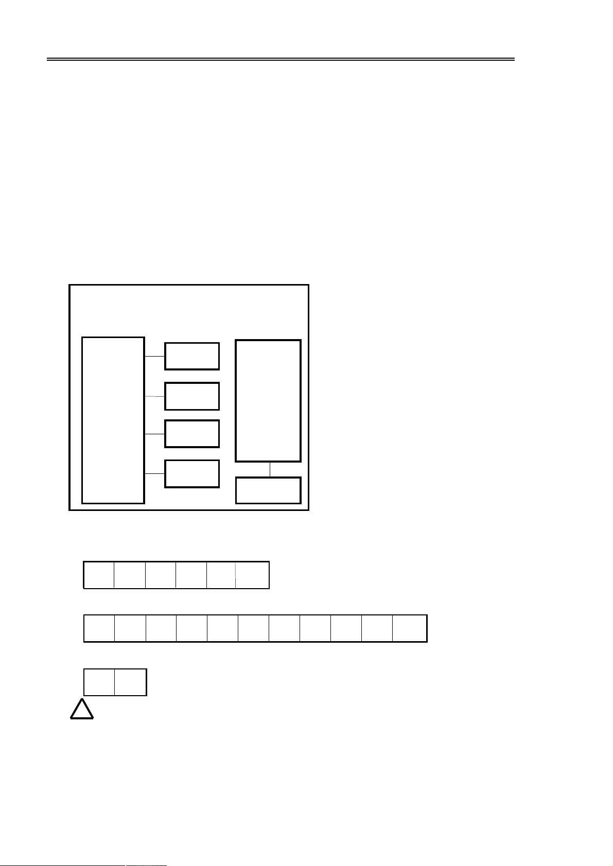
5V
PDAN/PDA/PDE/PDH Series
6 Digital
1.1 General description and Design philosophy
The PDAN Series inverter is a POWER CONVERTER for variable-speed AC drives. It applies the Sensor-less Vector
concept to control the output voltage and frequency to the motor. Use current sensor detects three phase AC current
signals and phase angle, and using the Sensor less Vector algorithm to compensate motor speed variation. The PDAN
series will provide more torque at low speed and automatic compensate the motor slip when under heavy loading.
The PDA Series inverter is a POWER CONVERTER for variable-speed AC drives. It applies the Sensor-less Vector
concept to control the output voltage and frequency to the motor. Use only one current sensor at DC bus, the advanced
microprocessor detects the DC current and recovers the signal into three phase AC current signals. Phase angle of the
output current is measured in order to compensate motor speed variation using the Sensor less Vector algorithm.
Superior than traditional V/F inverter, the PDA series will provide more torque at low speed and auto compensate the
motor slip when under heavy loading.
PDE series inverter is similar to PDA series. However, for economic reason, a simple shunt resistor replaces the Halleffect current sensor. Therefore, the PDE does not include all the functions involving current measurement and
calculation.
The PDAN, PDA and PDE inverters can generate output frequency up to 650Hz.
PDH series inverter can generate output frequency up to 3,000Hz used for driving very high-speed motors. In order to
decrease sub-harmonic when running the motor at high frequency, it employs Synchronous Symmetric Sine Pulse
Width Modulation method for waveform generation.
Input
3 Digital
Output
3 Analog
Inputs
Up/Down
Counter
TIMER
Flip/Flop
Auto-Run
0~650Hz
SensorLess
Vector
IGBT
Inverter
* RS-232/485
Built in standard UP/DOWN Counter Module,
Timer/Counter Module and Flip/Flop Module that are
very often used in actual application system.
Six digital inputs and three digital outputs are all
programmable to meet all kinds of applications.
Three analog inputs AI1, AI2 and AI3 is provided for
various control applications. Moreover, many combinations
of these three AIx signals are provided; allow your system
design flexible.
Serial communication control software is embedded in
the CPU; it can easily achieve computer direct control
through RS485 serial port. It is very useful when inverter or
many inverters would like to be dynamical controlled by
master computer. With repeater one serial port can
address up to 99 inverters. (Standard RS485 driver can
drive up to 31 inverters only.)
* The PDAN series inverter has built-in RS-485 interface;
the RS-485/RS-232 option card is available for PDA/PDE
/PDH series inverter.
1.2 Control input & output configuration
The control terminal on the CPU board can be separate into three groups.
Terminal for Analog signals:
AM AI1
*AI3 does not exist in PDA/H-4015, PDE-2007/2015.
Terminal for Digital signals:
DI1
*RUN=DI5, REV=DI6
Terminal for 1a contact Relay output:
RY2
RY1
!
CAUTION
All the input/output control signal lines, or remote panel lines and communication lines must be laid separately from the
high current power/motor/brake lines.
They must not be fed through the same cable conduit/trucking.
DI2
AI2 AI3
DI3 DI4
RUN
ACOM
REV
RST
DO1 DO2
24V
DCOM
Page 5
4
1.2.1 Analog input blocks (Refer to Sec. 7)
AI1input
AI2 input
AI3 input To CPU
AI3 terminal
AM
l AI1, AI2 and AI3 are analog input terminals.
l AM terminal is used for analog signal output.
l ACOM is the common terminal for analog circuit.
l The 5V terminal supply analog +5V.
l Inside the control board, there are three jumpers JP1, JP2 and JP3. They are used for selecting the hardware
configuration of AI1, AI2 and AI3 respectively.
Note: there are only two jumpers JP1 and JP2 in PDA/H-4015, PDE-2007/2015.
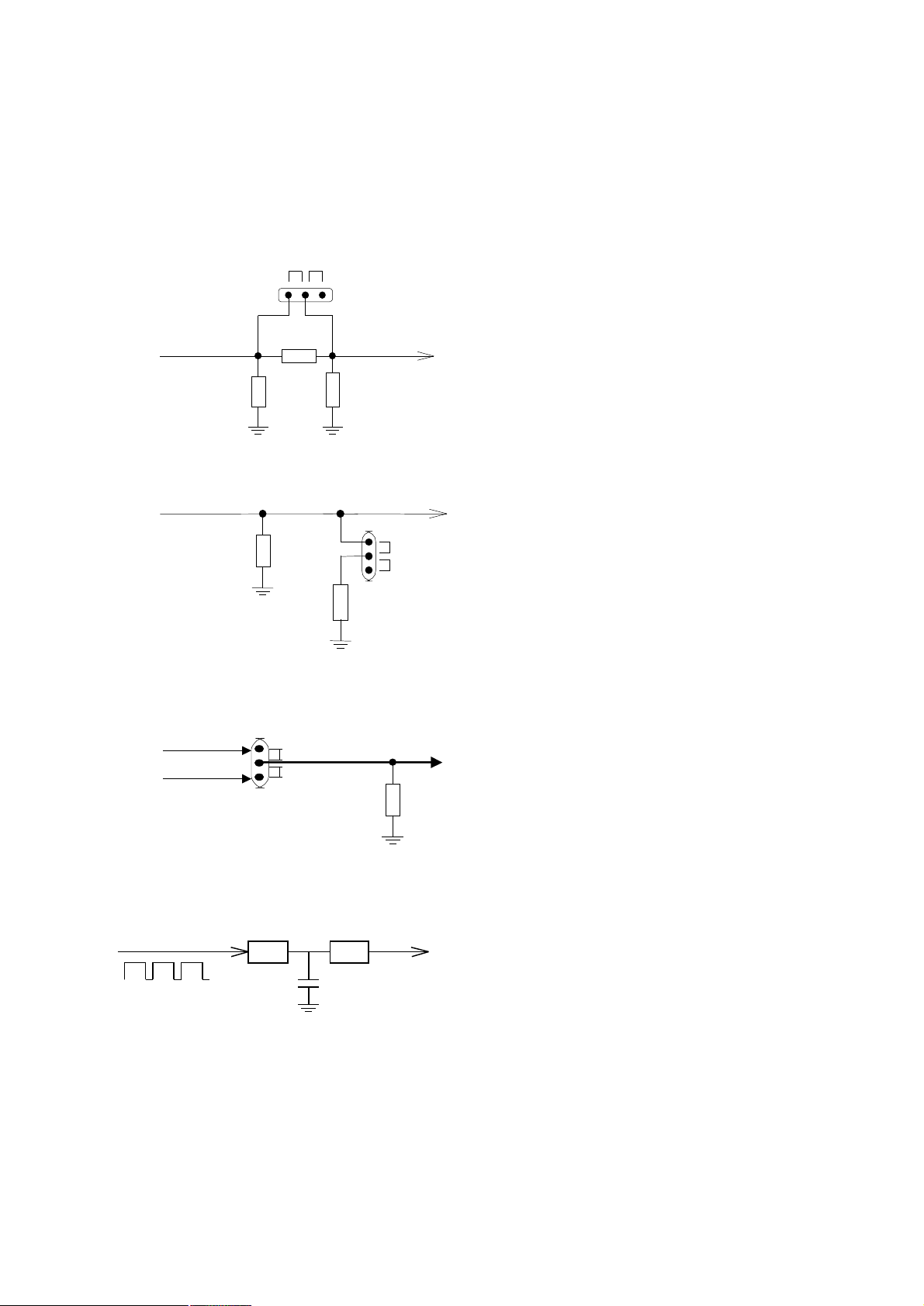
1.2.1.a Analog input AI1 module
+10V+5V
JP1
22k
To CPU
22k
JP1 is used to define the characteristic of the input terminals
AI1.
l If you are using external analog voltage 0 ~ +10V input,
please use AI1 and select JP1 to +10V position.
l If you are using external analog voltage 0 ~ +5V input to
AI1, select JP1 to +5V position.
1.2.1.b Analog input AI2 module
To CPU
20mA
+5V
JP2
249
JP2 is used to define the characteristic of the input terminal
AI2.
l If you are using 0 ~ +5V input (external or internal
voltage reference) to AI2, select JP2 to +5V position.
l If you are using external 20mA current input to AI2,
must select JP2 to 20mA position.
1.2.1.c Analog input AI3 module
JP3
Panel VR
PAN
TER
The LOCAL panel has built in a small potential meter VR.
Through jumper JP3, user can select the input source of AI3
either from terminal or from panel.
For models PDA/H-4015, PDE-2007/2015, because there is no
AI3 input terminal, the CPU always connects to panel VR.
1.2.2 AM the Analog output module (Refer to Sec.10)
PWM Waveform
from CPU
Width proportional
to desire voltage
1k
820uH
LR
C
The output voltage of AM terminal comes from CPU in PWM
waveform. Its duty cycle is proportional to the desired analog
amplitude. And the signal is filtered by internal resistor R and
capacitor C.
Page 6
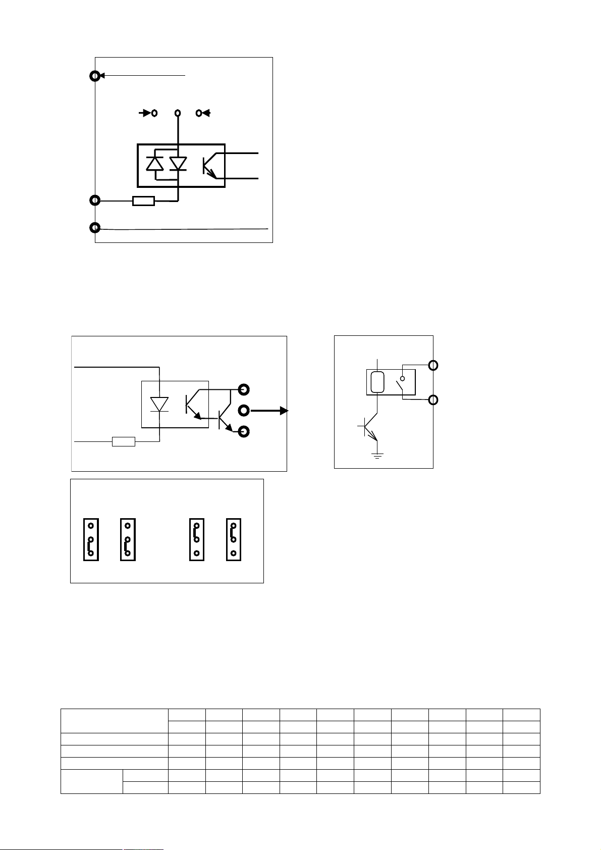
5
1.2.3 Digital Input terminals (DI1 ~ DI4 and RUN / REV)
DO1,2
NPN type DI/DO
+24V
RY2
5V
24V
DCOM
Sink/Source jumper
+24V
l DI1~DI4, RUN, REV are all identical Bi-directional digital
inputs.
RUN terminal is equal to DI5.
REV terminal is equal to DI6.
l +24V is common power supply for all DIx.
l DCOM is the command reference for these digital circuits.
l Each Digital Input can be configured individually by
To CPU
corresponding parameter. Refer to section 6, 8.
l User can select Sink (NPN) type or Source (PNP) type by
GND
jumper JP4 and JP5.
Note: The minimum input signal width is 5ms.
DI1~6
DCOM
4.7k
Common line of +24V
1.2.4 Digital Output terminals (Refer to Sec. 9)
There are three digital output signals available to the user. Two of them are designed as open collector output; another
is voltage isolated "1a" contact of relay output.
l Open collector outputs are named as DO1 and DO2, DCOM is the common point.
l The relay output is terminals RY1, RY2 (Note RY1, RY2 should drive 24V relay only.)
l Each Digital output can be configured individually by corresponding parameter. Refer to section 9.
Open Collector output
Signal
from CPU
Sink/Source Select jumper
DI/DO select PNP or NPN type
JP4
JP5
JP4
or
PNP type DI/DO
1.2.5 Hardware RESET terminal (RST)
The input hardware structure is similar to digital inputs described in Sec.1.2.3.
Terminal RST is used for reset the inverter.
l If Sink (NPN) type selected, under any circumstances, RST and DCOM shorted together will force the inverter
execute RESET, as if Power On again.
l If Source (PNP) type selected, under any circumstances, RST and 24V shorted together will force the inverter
execute RESET, as if Power On again.
1.3 Electrical Specifications
Model
PDAN/PDA/PDE/PDH -
HP 1 2 3 5 7.5 10 15 20 30 40
KW 0.75 1.5 2.2 3.7 5.5 7.5 11 15 22.5 30
KVA 2.0 3.0 4.0 6.5 9.5 13 19 25 34 46
-2xxx 5 7 11 17 24 33 46 61 90 Amp rms.
-4xxx - 4.0 5.5 8.5 12 17 23 31 45 57
2007 2015 2022 2037 2055 2075 2110 2150 2225 2300
- 4015 4022 4037 4055 4075 4110 4150 4225 4300
JP5
RY1
l JP4 upper position selects Source (PNP) input
l JP5 upper position selects Source (PNP) output
l JP4 lower position selects Sink (NPN) input
l JP5 lower position selects Sink (NPN) output
Note: The digital input terminals and digital output terminals of
PDA/H-4015, PDE-2007/2015 are “NPN” type only, there are no
JP4 and JP5 on CPU board.
Page 7
6
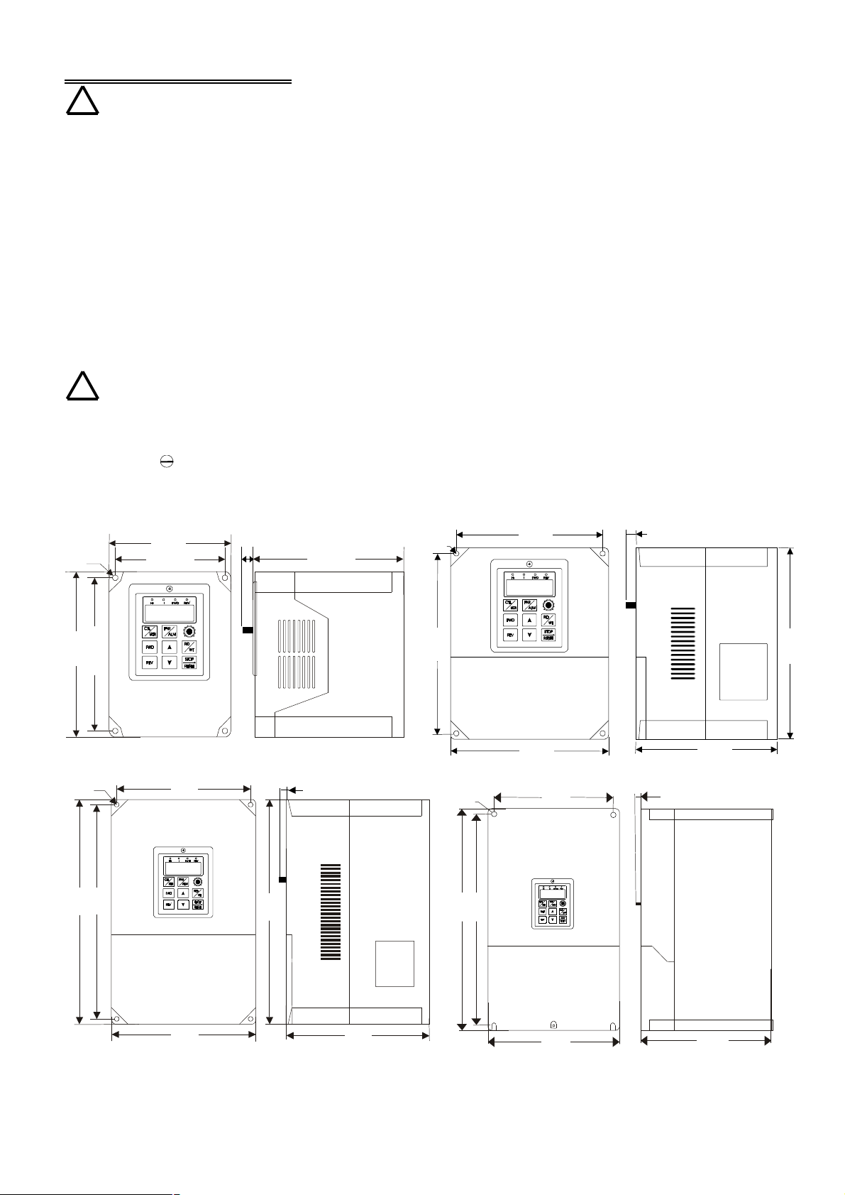
2 INSTALLATION
PDx - 2007、2015、4015
10.0
170.0
157.6
193.6
152.2
10.0
206.0
PDx - 2022、2037、4022、4037
420
250
248
226
10.0
400
Ø
178
190
Ø6.0
192
10.0
!
WARNING
l To guarantee the safe operation of the equipment it must be installed and commissioned properly by qualified
personnel in compliance with warnings laid down in these operating instructions.
l Take particular note of the general and regional installation and safety regulations regarding work on high
voltage regulations, as well as the relevant regulations regarding the correct use of tools and personal protective
gear.
l Make sure that the unobstructed clearance for each of the cooling inlets and outlets above and below the inverter
is at least 100mm.
l Make sure that a space of 40mm is kept free at the sides of the inverter to permit the cooling air to escape from
the side slits.
l Ensure that the temperature does not exceed the specified level when the inverter is installed in cubicle.
l Avoid excessive vibration and shaking of the equipment.
l Do not be obstruct the cooling fan that installed on the inverter, it is used to build proper airflow for heat sink
thermo dissipation. And do not touch the fan hole when it is running.
NOTE: Please consider the possible use of options, such as RFI suppression filters at the planning stage.
!
CAUTION
1) To open the upper cover of the inverter, follow these rules :
2) Cut off the input supply power
3) Wait 5 minutes until internal capacitor completely discharged
4) Use small minus screw driver, plug into the lock holes located at the lower edge of the cover. Then the cover
is free to open.
2.1 Outline Dimensions
125
Ø 5.5
170
157.5
286 300
112.5
300
154.5
Ø5.5
8.0
PDx - 2055、2075、4055、4075
PDx - 2110、2150、2225、4110、4150、4225
Page 8
7
2.2 Power Terminal
The upper cover must be removed in order to connect the electrical leads.
Basically, the Power terminals are divided into three portions:
l The Power line input, (R, S, T) receives power for the operation of the inverter.
l The Motor line output, (U, V, W) delivers Variable Frequency output to motor leads.
l Brake resistor connect to B, P, terminal. (The inscription of terminals may be PR or PB.)
Note: Must connect Earth properly.
!
WARNING: Never connect power line to U, V, W, P, N, B, PR, BR.
2.3 Connect Power line input to Inverter
!
WARNING and CAUTION
l Between the power line and the inverter, add NFB for system protection.
l There are static sensitive components inside the Printed Circuit Board. Avoid touching the boards or
components with your hands or metal objects.
l Only the terminal screws may be touched with the insulated screwdrivers when connecting the leads.
l Make sure to connect the power terminals tight and correctly.
l Make sure that the power source supplies the correct voltage and is designed for the necessary current.
l Make sure the motor is configured to match the input voltage.
l Protective EARTH terminal marked with must be connected properly.
l Take care that the appropriate circuit breakers with the specified current rating are connected between the
power supply and the inverter.
2.4 Connect inverter output to Motor
!
WARNING
Do not insert contactors between inverter output and motor.
For every model, "U, V, W " are the three phase output terminals, they should be connected to motor leads
directly.
2.5 Control terminal connection
!
CAUTION
All the input/output control signal lines, or remote panel lines and communication lines must be laid separately
from the high current power/motor/brake lines. They must not be fed through the same cable conduit/trucking.
Page 9
8
2.6 DC bus terminal (P, N) or Brake terminal (B, P)
!
CAUTION
Some models with power terminal marked P and N, these models does not include Brake transistor inside the inverter.
Customer may use extra Brake Transistor Module for discharge brake function.
For models that include braking transistor, the power terminal will mark P and B. User can connect suitable resistor to
the P & B terminals directly.
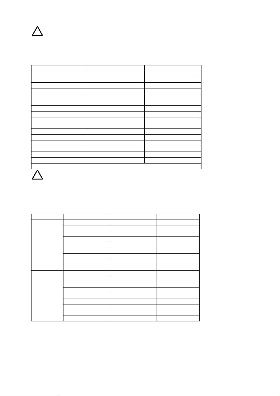
Here is the recommended table for discharge resistors:
Model Resistance (Ohm) Rating (Watt)
2007 200 80
2015 100 150
2022 60 250
2037 40 300
2055 30 500
2075 20 600
2110 15 1000
2150 10 1500
4007 750 80
4015 400 150
4022 250 250
4037 150 300
4055 100 500
4075 75 750
4110 50 1000
4150 40 1500
Discharge duty 10%
!
Warning:Never connect resistor to P & N terminal
If the terminals are P & N, must add external braking unit.
2.7 A.C.L.
When power supply capacity is larger than 500KVA and/or using thyrister, phase advance capacitor etc. from same
power supply, must fitting A.C.L. at R.S.T. power input side to curb instantaneous current and to improve power ratio.
Here is the recommended table for A.C.L.:
Voltage (V) Model Current (Arms) Induction Value
2007 6 1.8mH
2015 10 1.1mH
2022 15 0.71mH
2037 20 0.53mH
220
380/440
Note: The A.C.L. for 220V and 380V/440V have different induction values, please does not mix up.
2055 30 0.35mH
2075 40 0.26mH
2110 60 0.18mH
2150 80 0.13mH
2225 120 0.09mH
4015 5 4.2mH
4022 7.5 3.6mH
4037 10 2.2mH
4055 15 1.42mH
4075 20 1.0mH
4110 30 0.7mH
4150 40 0.53mH
4225 60 0.36mH
4300 80 0.26mH
Page 10
9
3 CONTROL PANEL
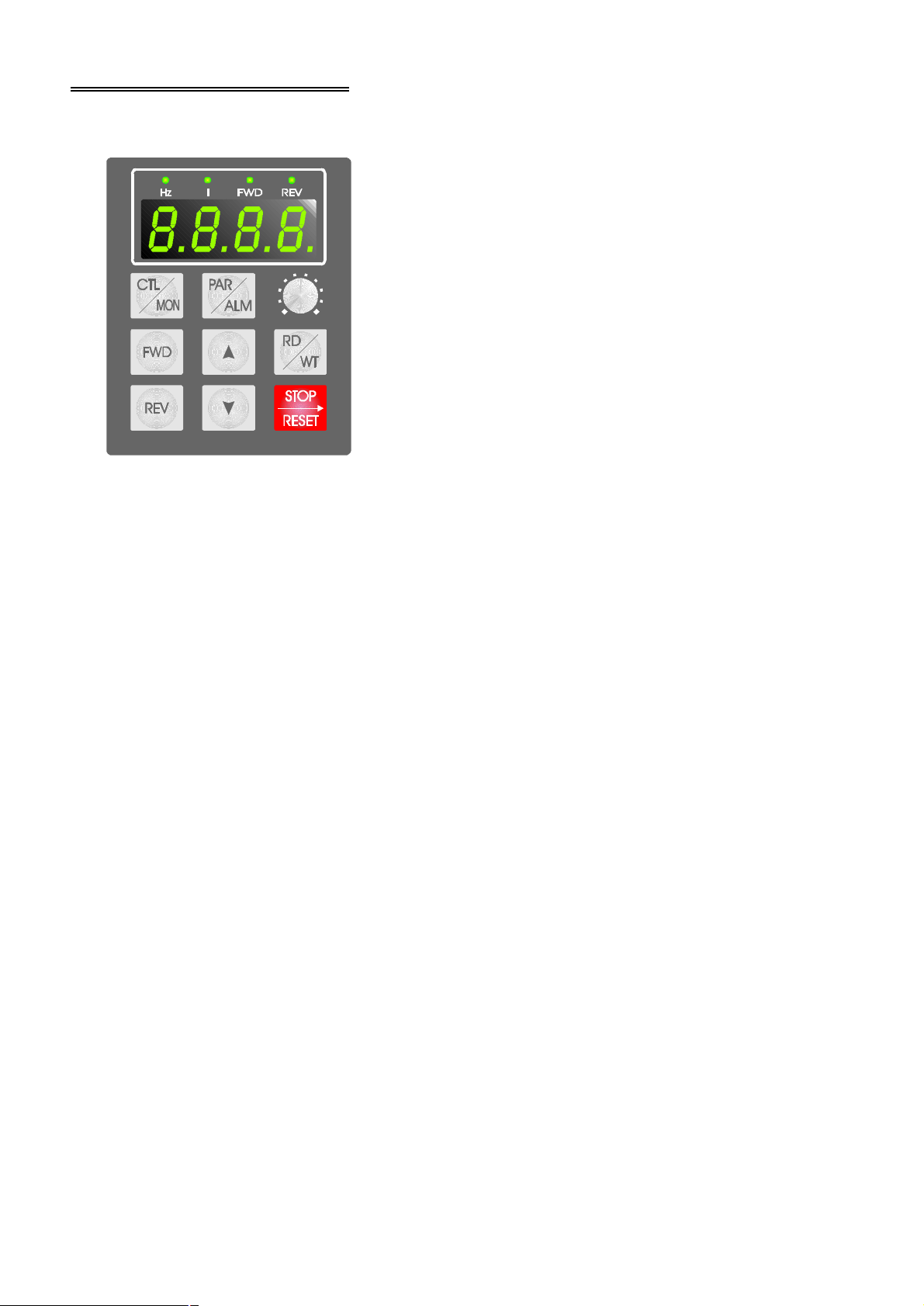
The control panel involves 4 digits 7-segment display and 4 Led-lamps, 8 keys and a potential meter (VR).
It has four possible operation modes: "CTL", "MON", "PAR" and "ALM modes, described below.
3.1 CTL mode
VR input is equivalent to AI3 input.
Push the "CTL/MON" key, will change the keypad operation between "CTL"
and "MON" Mode.
If both "HZ" and "I" Led are blank, it is under "CTL" Mode.
Under "CTL" Mode, user can control the inverter running in either direction
and may modify the desired running speed.
For normal run/stop control, use only the three keys:
FWD key is used for running the inverter in forward direction.
REV key is used for running the inverter in reverse direction.
STOP key is used to stop the inverter.
If Pr.40=3 or 8, the running frequency shall be modified by keypad, then these
keys are enabled:
RD/WT key is used to read out the data in Pr.00 (minimum value is Pr.16)
▲ key is used to increase the set frequency or the data read from Pr.00.
▼ key is used to decrease the set frequency or the data read from Pr.00.
STOP key is used for cursor shift
Procedure:
a. Under normal CTL mode, push RD/WT will enter Set Frequency mode, the display will show the value stored in
Pr.00 and blinking the data.
b. Push ▲ or ▼, the display starts to show the cursor position.
c. Push ▲ or ▼, in order to modify the Panel set frequency.
d. Push CTL/MON key will go back to normal CTL mode.
Note: If Pr.40=8, the newly modified Set Frequency will write into Pr.00 automatically.
3.2 MON mode
Push the "CTL/MON" key, will change the keypad operation between "CTL" and "MON" Mode.
Under "MON" Mode, user can control the inverter running in either direction and may monitor any two internal status
easily. (Refer to Sec.13)
If "HZ" Led is on, it is under "MON" Mode and 7-segment shows the "HZ" data. (Or the desired parameter assigned
by Pr.99)
If "I" Led is on, it is under "MON" Mode and 7-segment shows the "I" data. (Or the desired parameter assigned by
Pr.98)
FWD key is used for running the inverter in forward direction.
REV key is used for running the inverter in reverse direction.
STOP key is used to STOP the inverter.
▲ key is used to select "HZ" or "I" data shown on the 7-segment display.
▼ key is used to select "HZ" or "I" data shown on the 7-segment display.
3.3 PAR mode
Push the "PAR/ALM" key, will change the keypad operation between "PAR" or "ALM" mode.
If push PAR/ALM key, 7-segment shows "Pr.xx", it is under "PAR" Mode.
If push PAR/ALM key, 7-segment shows "0.-xx", it is under "ALM" Mode.
For PDA/E series, under PAR mode, the HZ and I lamps all ON.
Under "PAR" Mode, user can modify or monitor all the internal PARAMETERS.
To modify a parameter, follow the steps described below:
STEP 1: push "PAR/ALM" key, the 7-segment will show "Pr.nn". (nn is parameter number)
STEP 2: push ▲ or ▼ key to select desired parameter number, and "STOP" key used as cursor shift.
STEP 3: push "RD/WT" key to READ the content of the specified parameter.
The 7-segment now shows the value of this parameter.
STEP 4: push ▲ or ▼ key to modify the displayed value, and "STOP" key used as cursor shift.
STEP 5: push "RD/WT" key to WRITE the new value into parameter memory.
STEP 6: push "PAR/ALM" repeat STEP 1 to modify next parameter.
3.4 ALM mode
Push the "PAR/ALM" key, will change the keypad operation between "PAR" or "ALM" mode.
If push PAR/ALM key, 7-segment shows "0.-xx", it is under "ALM" Mode.
Under "ALM" Mode, the user can execute RESET function or monitor ALARM STATUS.
STOP/RESET key, the inverter will execute RESET function.
▲ and ▼ key are used to check ALARM History.
Page 11
10
4 SYSTEM START-UP
Many operation methods were designed into the PDA/E/H Series inverter. Here in this section, teaching you how to start
running the inverter by simplest operation method.
4.1 Reset & Initialize the inverter
When you first receiving the inverter, and not sure of the parameter value inside the inverter, please execute Memory
Initialization. The initialization sequence is first set Pr.94=1(refer to section 3 and 5.3), then change to ALM mode
until display show 0. xx. Then push STOP/RESET key to start executing software reset and memory initialization.
Or, after Pr.94=1, then connect RST terminal to DCOM, and then Inverter will execute hardware RESET immediately.
After memory initialized, most parameters (marked with TYPE: R/W in Table 5.1) will be preload to the default values.
4.2 Setup Basic Motor Parameter
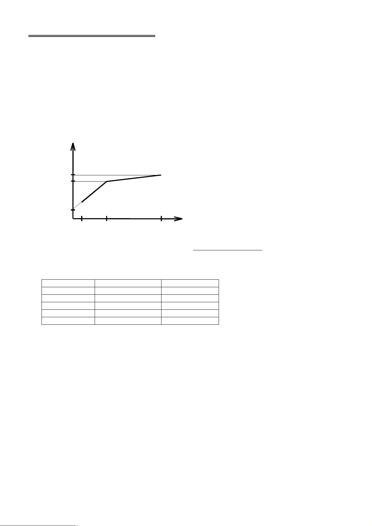
Firstly, before starting, basic V/F curve parameters must setup first. Refer to section 5.4, the description of Pr.09, Pr.10,
Pr.11, Pr.15, Pr.16 and Pr.88.
Vout
Pr.88(%)
Pr.11(%)
Pr.09(%)
Foutput
Pr.16(Hz)
Note: If Auto-Tuning had been executed, Pr.09 may be altered automatically.
Secondly, set motor rating is calculated from:
Pr.10(Hz) Pr.15(Hz)
=
gCurrentMotorRatin
%100*)(78.Pr
ttingCurrenInverterRa
4.3 PDA series Operation Mode Selection
For PDA series only, through Pr.67 selection, the inverter can operate under the following 5 different modes:
Operation Mode Description Series
Model 0 Standard V/F (I) PDA/PDE/PDH
Model 1 Standard V/F (II) PDAN/PDA/PDH
Model 2 Sensor-Less (I) PDA
Model 3 Sensor-Less (II) PDAN/PDA
Model 4 Power-Control Mode PDAN/PDA
4.3.0 Standard V/F (I) (For PDA/PDE/PDH)
Pr.67=0: The inverter delivers Sine PWM voltage waveforms to the motor winding. The current signal is used for
protection only. Output current waveform is not compensated by the feedback current signal.
Note: PDE series also operate under this mode.
4.3.1 Standard V/F (II) (For PDAN/PDA/PDH)
Pr.67=1: The inverter delivers Sine PWM waveform to motor, and check AC side output current. The distortion of
AC side current waveform due to IGBT dead time effect will be compensated in order to minimize torque ripple.
4.3.2 Sensor-Less (I) (For PDA)
Pr.67=2: When the inverter is running, it checks the output voltage, output current and the phase angle continuously.
If the motor speed changes because of loading effect, the inverter can modify its output frequency automatically.
4.3.3 Sensor-Less (II) (For PDAN/PDA)
Pr.67=3: Similar to Sensor-Less (I), the inverter operates under Sensor-less control algorithm.
Moreover, extra boost voltage is added in order to decrease the motor slip when running at low speed.
Page 12
11
4.3.4 Power (Torque) control (For PDAN/PDA)
·
=
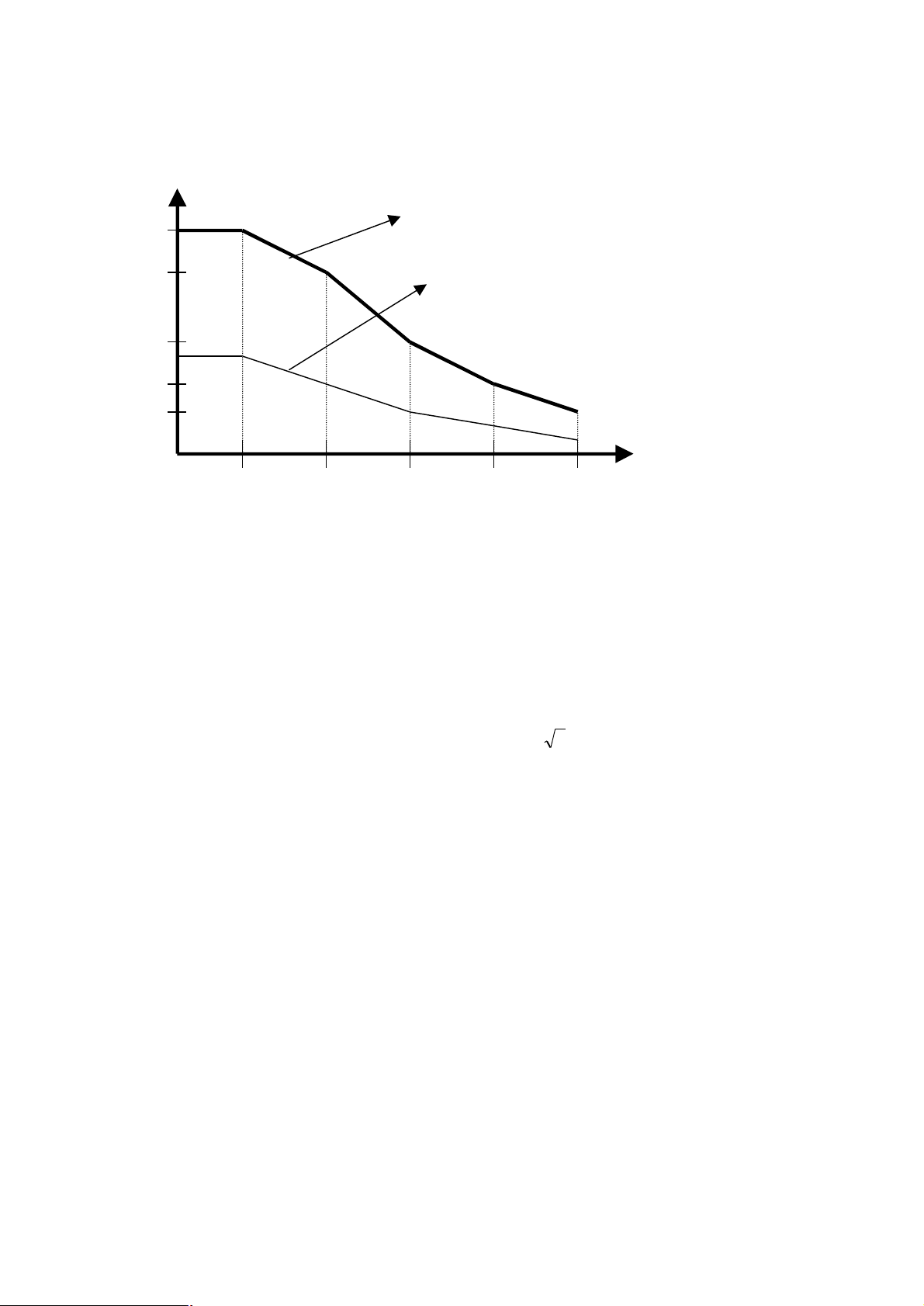
Pr.67=4: Basically its operation characteristics is similar to Pr.67=1. Moreover, the user can pre-assign the POWERLIMIT curve. Whenever the inverter output power exceeds the pre-defined limit curve, the output frequency will
decrease automatically. In addition, by using AI2 (or AI3), it is easy to modify the POWER-LIMIT curve
proportionally.
Note: In this mode, Pr.73~Pr.77 is used to define POWER LIMIT CURVE
Watt
POWER LIMIT CURVE
PL20
PL40
Proportionally modified by AI2 or AI3
PL60
PL80
PL100
Hz
20%
The POWER LIMIT CURVE can be modified by AI2 or AI3, refer to section 8.75.
Pr.72 should set to 0, because AUTO RUN function is not allowed.
PL20 (Pr.73): the POWER LIMIT value when Hzout=20% * Upper limit (Pr.15)
PL40 (Pr.74): the POWER LIMIT value when Hzout=40% * Upper limit (Pr.15)
PL60 (Pr.75): the POWER LIMIT value when Hzout=60% * Upper limit (Pr.15)
PL80 (Pr.76): the POWER LIMIT value when Hzout=80% * Upper limit (Pr.15)
PL100 (Pr.77): the POWER LIMIT value when Hzout=100% * Upper limit (Pr.15)
All PL20~PL100 parameters are expressed as “W.n”, which stands for
For example, if Pr.15=60Hz, PL20 (Pr.73)=15.2, it means the power limit at 12Hz(60Hz*20%) is:
2
=·=
The actual output power: PDA series is calculated from IdcVcapwattP
40% 60% 80% 100%*Pr.15
WattPL 1500101520
)(
WPL 10·=
n
PDAN series is calculated from
Refer to detail explanation of Pr.54 for monitoring the output current or power.
q
cos3)( ···= IoutVoutwattP
4.4 Auto Tuning
4.4.1 Auto Tuning for PDA series
For PDA series, the embedded Auto-Tuning program can search the internal characteristics of motor. For convenience
Both Dynamic Tuning and Static Tuning programs are installed.
Before start auto-tuning process, these parameters should be assigned first:
Pr.01: Main Acceleration rate
Pr.02: Main Deceleration rate
Pr.10: Base frequency (Hz) of the motor
Pr.11: Voltage (%) when the inverter output frequency reaches Base Frequency
Pr.12: Maximum Switching carrier
Pr.13: <=2.0 (KHz)
Pr.14: >=(Pr.10)÷2
Pr.15: Maximum frequency >= Pr.10
Pr.68: Sensor-Less Boost=0.0
Pr.88: Voltage (%) when the inverter output frequency reaches Upper Frequency
Pr.78: Current Rating (%) of the motor = (Motor Full Load current / Inverter Full Load current)*100%
4.4.1.1 PDA Dynamic Tuning
Set Pr.94=155, and reset the inverter, then the inverter will show “Auto” on the keypad, waiting to accept “FWD”,
“REV” or “STOP” command.
If push “FWD”(or REV), the inverter will start tuning process and motor running in forward (or reverse) direction.
Wait about 2minutes, when the motor characteristics obtained, the inverter will stop the motor and then initialize
itself automatically.
If push “STOP” key while tuning is in progress, the inverter will stop the motor immediately and show “Er.tu”.
Page 13

12
4.4.1.2 PDA Static Tuning
f
=
Set Pr.94=55, then reset the inverter, then the inverter will show “Auto” on the keypad, waiting to accept “FWD”,
“REV” or “STOP” command.
In push “FWD” or “REV”, the inverter will start tuning process by injecting direct current into the motor windings.
And while tuning, the motor should remain standstill throughout the entire tuning process.
If push “STOP” key while tuning is in progress, the inverter will stop the motor immediately and show “Er.tu”.
4.4.1.3 PDA Sensor-less related parameters
After tuning, these parameters are subject to change according the tuning results:
Pr.09 is general voltage boost value.
Pr.67 is RUN mode selection parameter
If tuning complete, Pr.67 will be set to 3, select Sensor-Less (II) compensation mode.
If tuning failed, Pr.67 will be set to 1, select standard V/F (II) mode.
Pr.68 is special voltage compensation factor
If tuning complete, Pr.68 will be used for Sensor-less voltage compensation.
If tuning failed, Pr.68 will be default to 5.0
Pr.69 is special frequency compensation factor
If tuning complete, Pr.69 will be used for Sensor-less compensation
If tuning failed, Pr.69 will be default to 50.50
4.4.1.4 PDA Tuning Fail process
When tuning process initiated, the display will show “Auto” and flashing. If push “STOP” key during this period,
the tuning process will be terminated immediately, and display will show “Er.tu” means Tuning Error.
If Error Tuning occurs, contents of these parameters will be default value.
Pr.09 = 3
Pr.67 = 1
Pr.68 = 5.0
Pr.69 = 50.50
4.4.2 Auto Tuning for PDAN series
For PDAN series, the embedded Auto-Tuning program can search the internal characteristics of motor.
Before start auto-tuning process, these parameters should be assigned first:
Pr.01: Main Acceleration rate
Pr.02: Main Deceleration rate
Pr.10: Base frequency (Hz) of the motor
Pr.11: Voltage (%) when the inverter output frequency reaches Base Frequency
Pr.15: Maximum frequency >= Pr.10
Pr.68: Sensor-Less Boost=0
Pr.78: Current Rating (%) of the motor = (Motor Full Load current / Inverter Full Load current)*100%
Pr.88: Voltage (%) when the inverter output frequency reaches Upper Frequency
4.4.2.1 PDAN Tuning
l Set Pr.94=155
l Reset the inverter, the inverter will start tuning process
4.4.2.2 PDAN Sensor-less related parameters
After tuning, these parameters are subject to change according the tuning results:
Pr.09 is general voltage boost value.
Pr.67 is RUN mode selection parameter
If tuning complete, Pr.67 will be set to 3, select Sensor-Less (II) compensation mode.
Pr.68 is special voltage compensation factor
If tuning complete, Pr.68 will be used for Sensor-less voltage compensation.
Pr.69 is special frequency compensation factor
If tuning complete, Pr.69 will be used for Sensor-less compensation
4.4.3 Gain Adjustment
Under conditions when Tuning Error occurs, or when fine adjustment is preferred for compensation accuracy,
customer can modify Pr.69 manually by the procedures described follows:
Note: Pr.69 is composed of two factors: Pr.69 = F1. F2, separated by decimal point.
F1: Low speed Phase compensation factor
Set Pr.67=1 and Pr.54=3 (refer to section 13.1), run the inverter at 5% low frequency (e.g. if Pr.10=60Hz, 5%=3Hz),
Read the POWER ANGLEfat this frequency,
Then calculate F1 according the following equation: )tan(/501
F2: High-Speed Load regulation factor
Run the motor to desired high frequency (e.g. 60Hz), using tachometer to check the speed variation between no load
and full load, then adjust the gain constant F2 in order to minimize the load regulation.
F
Page 14
13
4.5 Monitor Selection
Use Pr.98 and Pr.99 to select desired variables that you wish to monitor.
Enter MONITOR mode using LOCAL Panel:
Select MON mode by push CTL/MON key.
Pushing the CTL/MON key will change the mode between CTL and MON mode.
It is easy to distinguish that when any one of Hz or I lamp is ON, the inverter is under MON mode; if Hz or I lamp
all OFF, the inverter is under CTL mode.
The ▲ & ▼ keys are used to select the desired variable shown on 7-segment display for monitoring.
4.6 Simple application example
4.6.1 Input Motor Parameters
If the Input Line voltage is 220V, and the motor in use is
Rated Voltage 200V
Rated Frequency 50Hz
Rated Current 9Amp.
Maximum output frequency 80Hz is desired
Choose inverter model PDA-2037 (220V, 11Amp).
Then, set the following parameters according to above conditions:
Pr.95=0 and Pr.96=1, allow parameter change
Pr.10=50.00Hz, set motor Rated frequency
Pr.11=91%, set motor Rated voltage 91%=(200V/220V)*100%
Pr.15=80.00Hz, set maximum output frequency
Pr.88=100%, set maximum output voltage at maximum frequency
Pr.78=82%, set the percentage of motor rating to inverter rating 82%=(9Amp / 11Amp)*100%
Refer to Sec.4.2
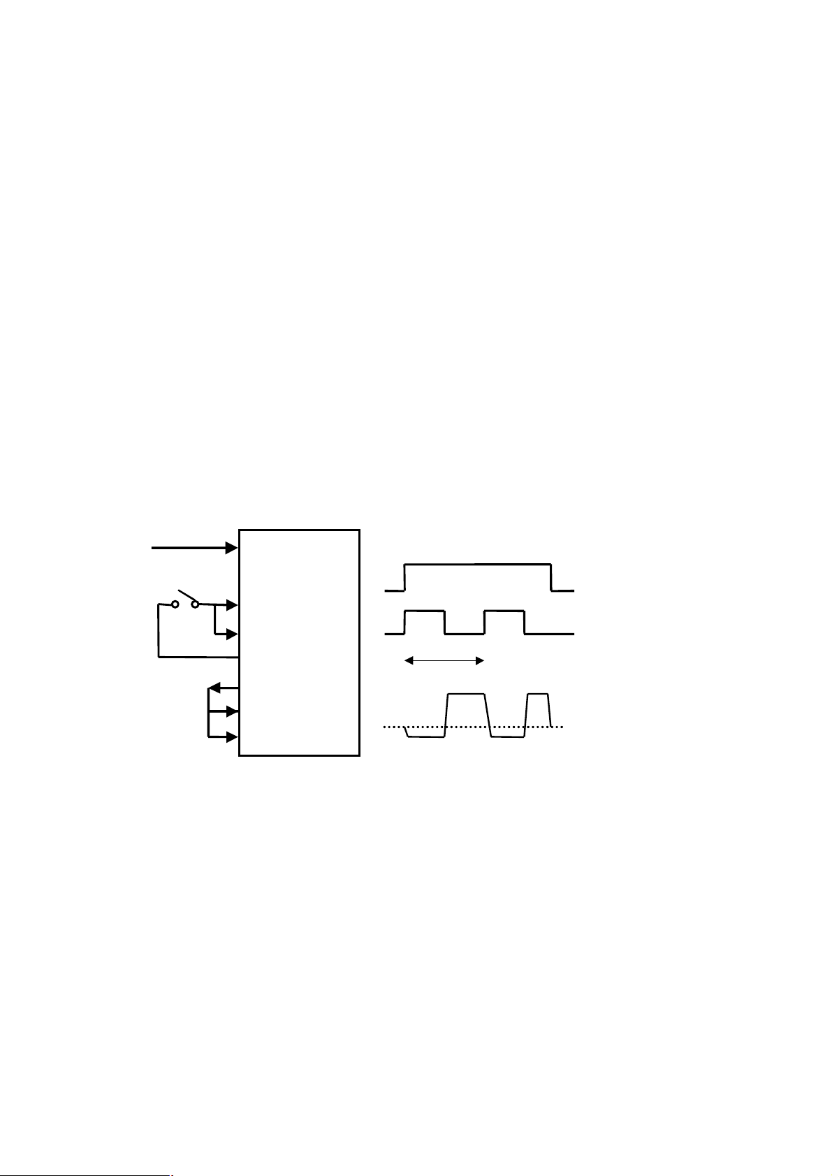
4.6.2 Application example
Panel VR
(AI3)
Start
DI5(RUN)
SW1
Set up procedure for above application:
l Pr.39=1.1 Determines the control command input from terminals
l Pr.40=25.00 Determines the set frequency may come from Panel-VR (AI3) or Pr.00
l Pr.00=60.00Hz Set predefined output frequency in Pr.00
l Pr.01=2.0Sec. Set desired acceleration time from stop to maximum speed
l Pr.02=2.0Sec. Set desired deceleration time from maximum speed to stop
l Pr.03=73 Select DI5 as RUN function
l Pr.04=74 Select DI6 as REV function
l Pr.41=36 Select DI1 as timer input
l Pr.42=88 Select DI2 as Frequency source switch (the function should combine with Pr.40). If DI2=OFF,
frequency source come from Panel-VR, else if DI2=ON, frequency source come from Pr.00
l Pr.45=43 Select DO1 as timer output
l Pr.71=20.0 Select timer ON/OFF period is 20seconds
Explanation:
l Define an auto ON/OFF timer with period equal 20seconds, using DI1, DO1 and Pr.41, 45, 71.
l When switch SW1 ON, starts inverter and enables the timer.
l The timer output will control motor forward or reverse and repeat every 20swconds.
l For the first 10seconds period, the inverter runs at 60Hz(Pr.00) reverse;
l For the second 10 seconds period, the inverter runs in forward direction with frequency determined by Panel-VR.
l When switch SW1 OFF, inverter stops.
DI1(TMIC)
DCOM
DO1(/TMOC)
DI6(REV)
DI2(88)
0V
Fwd
Rev.
Pr.71=20Sec.
AI3
Pr.00
Rev.
Page 15
14
5 PARAMETERS
5.1 Parameter List
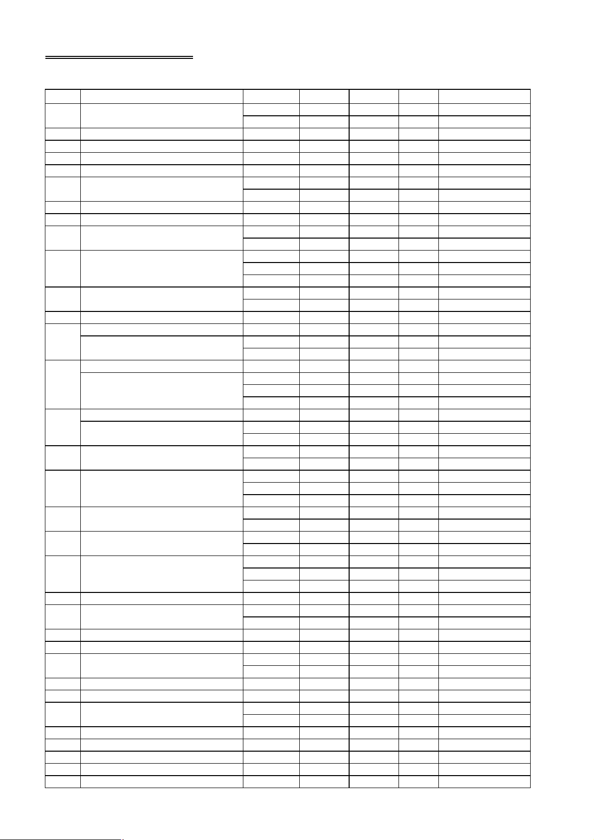
There are total 100 parameters in PDAN/PDA/PDE/PDH series inverter.
Pr.xx
Pr.00 MAIN SPEED SET
Pr.01 MAIN ACC TIME 10.0 Sec. 0.1 6553.0 R/W
Pr.02 MAIN DEC TIME 10.0 Sec. 0.1 6553.0 R/W
Pr.03 DI5 FUNCTION SELECT 73 0 99 FR/W
Pr.04 DI6 FUNCTION SELECT 74 0 99 FR/W
Pr.05 BRAKE FREQUENCY
Pr.06 BRAKE VOLTAGE 5 % 0 30 R/W
Pr.07 BRAKE TIME 1.0 Sec. 0.0 25.0 R/W
Pr.08 BRAKE DELAY TIME
Pr.09 BOOST VOLTAGE
Pr.10 BASE FREQUENCY
Pr.11 BASE VOLTAGE 100% 30 100 FR/W
Pr.12
Pr.13
Pr.14
Pr.15 UPPER FREQUENCY LIMIT
Pr.16 LOWER FREQUENCY LIMIT
Pr.17 SKIP FREQUENCY
Pr.18 SKIP WIDTH
Pr.19 JOG SPEED
Pr.20 JOG ACC/DEC 10.0 Sec. 0.1 25.0 R/W
Pr.21 SPD1 SPEED SET
Pr.22 SPD1 ACC TIME 10.0 Sec. 0.1 6553.0 R/W
Pr.23 SPD1 DEC TIME 10.0 Sec. 0.1 6553.0 R/W
Pr.24 SPD2 SPEED SET
Pr.25 SPD2 ACC TIME 10.0 Sec. 0.1 6553.0 R/W
Pr.26 SPD2 DEC TIME 10.0 Sec. 0.1 6553.0 R/W
Pr.27 SPD3 SPEED SET
Pr.28 SPD3 ACC TIME 10.0 Sec. 0.1 6553.0 R/W
Pr.29 SPD3 DEC TIME 10.0 Sec. 0.1 6553.0 R/W
Pr.30 FREE RUN STOP 0 0 1 R/W
Pr.31 REVERSE INHIBIT 0 0 1 R/W
Pr.32 POWER FACTOR & FILTER 85.20 50.00 99.99 FR/W PDAN
Parameter Name Default Min. Max. Type Remark
0.00 Hz 0.00 650.00 R/W PDAN/PDA/PDE
0.0 Hz 0.0 3000.0 R/W PDH
5.00 Hz 0.50 650.00 R/W PDAN/PDA/PDE
50.0 Hz 5.0 3000.0 R/W PDH
0.5 Sec. 0.1 1.0 R/W PDA/PDE/PDH
0.5 Sec. 0.0 1.0 R/W PDAN
3 % 0 30 FR/W PDAN
5 % 0 30 FR/W PDA/PDE
0 % 0 30 FR/W PDH
60.00 Hz 0.50 650.00 FR/W PDAN/PDA/PDE
600.0 Hz 5.0 3000.0 FR/W PDH
PWM Carrier/Carrier Transfer Point 16.0 KHz 2.0 16.9 FR/W PDAN
PWM_CARRIER
MODBUS ELAPSE TIME 3ms 3 250 FR/W PDAN
MINIMUM_CARRIER
THERMISTOR TYPE 440.8 0.0 999.9 FR/W PDAN
CARRIER_TRANSFER_POINT
16.0 KHz 2.0 16.0 FR/W PDA/PDE
18.0 KHz 2.0 18.0 FR/W PDH
2.0 KHz 0.5 16.0 FR/W PDA
0.5 KHz 0.5 16.0 FR/W PDE
2.0 KHz 2.0 18.0 FR/W PDH
30.00 Hz 0.00 650.00 FR/W PDA/PDE
300.0 Hz 0.0 3000.0 FR/W PDH
60.00 Hz 0.50 650.00 FR/W PDAN/PDA/PDE
600.0 Hz 5.0 3000.0 FR/W PDH
3.00 Hz 0.00 650.00 FR/W PDAN
3.00 Hz 0.50 650.00 FR/W PDA/PDE
30.0 Hz 2.0 3000.0 FR/W PDH
0.00 Hz 0.00 650.00 R/W PDAN/PDA/PDE
0.0 Hz 0.0 3000.0 R/W PDH
0.00 Hz 0.00 5.00 R/W PDAN/PDA/PDE
0.0 Hz 0.0 50.0 R/W PDH
10.00 Hz 0.00 650.00 R/W PDAN/PDA
10.00 Hz 0.50 650.00 R/W PDE
100.0 Hz 0.0 3000.0 R/W PDH
0.00 Hz 0.00 650.00 R/W PDAN/PDA/PDE
0.0 Hz 0.0 3000.0 R/W PDH
0.00 Hz 0.00 650.00 R/W PDAN/PDA/PDE
0.0 Hz 0.0 3000.0 R/W PDH
0.00 Hz 0.00 650.00 R/W PDAN/PDA/PDE
0.0 Hz 0.0 3000.0 R/W PDH
Page 16
15
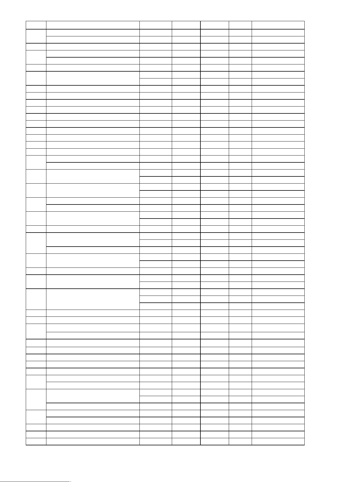
Pr.xx
Pr.33
Pr.34 UP/OP RESTART ENABLE 0 0 1 R/W
Pr.35
Pr.36 BASE BLOCK TIME 0.5 Sec. 0.1 5.0 R/W
Pr.37 AM SELECT
Pr.38 AM GAIN 255 0 255 R/W
Pr.39 CONTROL COMMAND SELECT 0.0 0.0 9.9 R/W
Pr.40 SPEED INPUT SELECT 8.08 0.00 99.99 R/W
Pr.41 DI1 FUNCTION SELECT 0 0 99 R/W
Pr.42 DI2 FUNCTION SELECT 0 0 99 R/W
Pr.43 DI3 FUNCTION SELECT 0 0 99 R/W
Pr.44 DI4 FUNCTION SELECT 0 0 99 R/W
Pr.45 DO1 FUNCTION SELECT 0 0 99 R/W
Pr.46 DO2 FUNCTION SELECT 0 0 99 R/W
Pr.47 RELAY FUNCTION SELECT 4 0 99 R/W
Pr.48
Pr.49 HZ DETECT LEVEL
Pr.50 HZ DETECT TOLERANCE
Pr.51
Pr.52 POLE
Pr.53 GEAR RATIO 100 % 0 100 R/W
Pr.54
Pr.55 A/D CHANNEL SELECT
Pr.56 A/D DATA 0 1023 M
Pr.57 HZ
Pr.58 RPM
Pr.59 Vdc (Capacitor) Vdc M
Pr.60 Vout (r.m.s. output) Vrms M
Pr.61
Pr.62 TEMPERATURE ℃ 0 100 M
Pr.63 Digital Input Terminal Status 0.0.0.0. 0.0.0.0. 1.1.1.1. M
Pr.64 RUN/REV INPUT STATUS 0.0. 0.0. 1.1. M
Pr.65 Digital Output Terminal Status 0.0.0. 0.0.0. 1.1.1. M
Pr.66 Reserve
Pr.67
Pr.68
Pr.69
Pr.70 ANALOG INPUT GAIN 50% 0 100 R/W
Pr.71 TIMER TIME 5.0 Sec. 0.2 6553.0 R/W
Pr.72 AUTO RUN MODE SELECT 0 0 6 R/W
Parameter Name Default Min. Max. Type Remark
DISCHARGE ENABLE 0 0 2 R/W PDAN/PDA/PDH
Reserve PDE
STALL LEVEL 200% 10 200 R/W PDAN/PDA/PDH
Reserve PDE
0 0 17 R/W PDAN
0 0 16 R/W PDA/PDE/PDH
Irms/Idc DETECT LEVEL 100% 0 150 R/W PDAN/PDA/PDH
Reserve PDE
30.00 Hz 0.00 650.00 R/W PDAN/PDA/PDE
300.0 Hz 0.0 3000.0 R/W PDH
5.0 Hz 0.0 25.0 R/W PDAN/PDA/PDE
50 Hz 0 250 R/W PDH
THERMAL TRIP TIME 60 Sec. 0 120 R/W PDAN/PDA/PDH
Reserve PDE
4 2 12 FR/W PDAN
4 2 12 R/W PDA/PDE/PDH
MONITOR SELECT
Reserve PDE
Irms, Idc and others
Reserve PDE
OPERATION MODE SELECT 1 0 4 FR/W PDAN/PDA
Reserve PDE/PDH
Sensor-Less Boost
Reserve PDE/PDH
SLIP constant F1/F2 50.50% 0.0 99.99 FR/W PDAN/PDA
Reserve PDE/PDH
0 0 250 R/W PDAN
0 0 27 R/W PDA/PDH
0 0 250 R/W PDAN
0 0 7 R/W PDA/PDE/PDH
Hz 0.00 650.0 M PDAN/PDA/PDE
Hz 0.0 3000 M PDH
rpm/Krpm 0.00 M PDAN
Krpm 0.00 M PDA/PDE
Krpm 0.00 M PDH
10 0 30 FR/W PDAN
5.0 0.0 20.9 FR/W PDA
M PDAN/PDA/PDH
Page 17
16
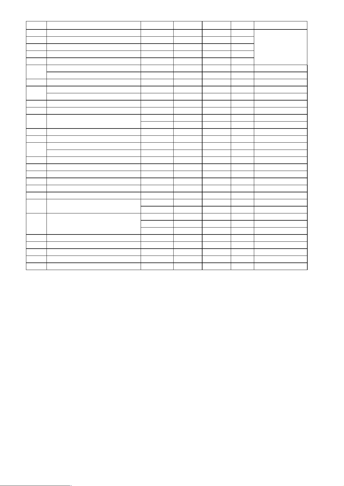
Pr.xx
Pr.73 AUTO STEP1 (or 6) PERIOD 15.0 Sec. 0.1 6553.0 R/W
Pr.74 AUTO STEP2 (or 7) PERIOD 15.0 Sec. 0.1 6553.0 R/W
Pr.75 AUTO STEP3 (or 8) PERIOD 15.0 Sec. 0.1 6553.0 R/W
Pr.76 AUTO STEP4 (or 9) PERIOD 15.0 Sec. 0.1 6553.0 R/W
Pr.77 AUTO STEP5 (or 10) PERIOD 15.0 Sec. 0.1 6553.0 R/W
Pr.78
Pr.79 RESTART TYPE SELECT 0 0 3 R/W
Pr.80
Pr.81 SPEED SEARCH DEC TIME 2.0 Sec. 0.1 25.0 R/W
Pr.82 VOLTAGE RECOVER TIME 0.5 Sec. 0.1 5.0 R/W
Pr.83 IGBT GUARD TIME
Pr.84 LINE VOLTAGE 40 1000 FR/W
Pr.85 RATED CURRENT 0.5 3000.0 FR/W
Pr.86
Pr.87 VDC ADJUST 70 140 FR/W
Pr.88 MAX. OUTPUT VOLTAGE 100% 30 100 FR/W
Pr.89 AI1 LOW 12 0 1023 FR/W
Pr.90 AI1 HIGH 1012 0 1023 FR/W
Pr.91 AI2 LOW 12 0 1023 FR/W
Pr.92 AI2 HIGH 1012 0 1023 FR/W
Pr.93 UNIT/PROTOCOL SELECT
Pr.94 RELOAD PARAMETER
Pr.95 MEMORY PROTECT 0 0 2 R/W
Pr.96 FACTORY WRITE ENABLE 0 0 1 R/W
Pr.97 VERSION R
Pr.98 MONITOR (I) 61 0 99 R/W
Pr.99 MONITOR (HZ) 57 0 99 R/W
Note:
1. Type R/W parameters are stored in EAROM memory. They can be read/write and store in the memory permanently.
2. Remark column shows the difference for specific parameter between each model. If it is blank, means this specific
Parameter Name Default Min. Max. Type Remark
Refer to Sec.4.3.4
for PDAN\PDA
torque mode, and
Appendix A for
PID function
MOTOR RATING 100% 10 100 FR/W PDAN/PDA/PDH
Reserve PDE
RESTART STALL LEVEL 150% 10 200 R/W PDAN/PDA/PDH
Reserve PDE
3.0 usec 2.0 25.0 FR/W PDAN
3.0 usec 2.0 25.5 FR/W PDA/PDE/PDH
IRMS ADJUST 100 70 140 PDAN/PDA/PDH
Reserve PDE
0.01 0.01 99.99 FR/W PDAN
0.01 0.01 7.99 FR/W PDA/PDE/PDH
0 0 250 R/W PDAN
0 0 255 R/W PDA
0 0 1 R/W PDH/PDE
Type FR/W parameters are also stored in EAROM memory. Generally, they are used for factory adjustment. Only
authorized engineers should modify them.
Type M is read only parameters for monitoring.
Type R is constant parameters.
parameter is same for all PDAN/PDA/PDE/PDH models.
5.2 Parameter Protection
Pr.95 -- MEMORY PROTECT
Pr.96 -- FACTORY WRITE ENABLE
If set Pr.95=1, all parameters (except Pr.00 and Pr.95 itself) are not allow to change.
If set Pr.95=0, parameters with R/W type are allowed to change.
If set Pr.95=0 and Pr.96=1, all parameters include FR/W type can be modified.
PDAN series: If set Pr.95=2, any further parameter change will write to RAM only, they will be changed to original
value after RESET or power off.
5.3 Parameter Initialization
5.3.1 Initialize data into R/W type parameters
Note: parameters with FR/W type will not be initialized by this method.
Follow the process to execute memory initialization
Step 1: Write Pr.95 = 0, and Pr.94 = 1
Step 2: Execute "ALM" RESET
or Step 2: Execute Hardware RESET
or Step 2: Execute Power-On RESET
After initialization process, the data in EAROM memory (R/W type) will change to the DEFAULT values listed in the
PARAMETERS LIST Table.
Page 18
17
5.3.2 Initialize data into ALL parameters (for PDAN series only)
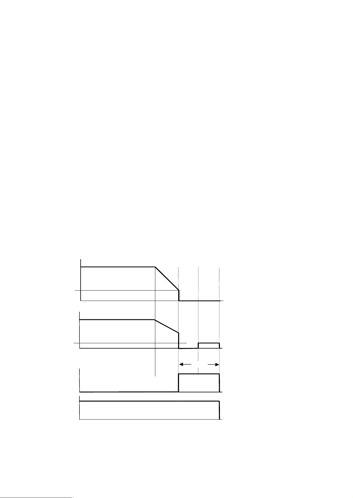
HZ A B C D time time Pr.08
Pr.06
TIMING RELATIONSHIP BETWEEN HZ & VOUT WHILE BRAKING STOP
VOUT(%)
time BRAKING
signal out
DOx
DOx_SELECT = 6
time
signal out
DOx
DOx_SELECT = 7
Pr.07
Follow the process to execute memory initialization
Step 1: Write Pr.95 = 0, and Pr.94 = 249
Step 2: Execute "ALM" RESET
or Step 2: Execute Hardware RESET
or Step 2: Execute Power-On RESET
After initialization process, all of data in EAROM memory will change to the DEFAULT values listed in the
PARAMETERS LIST Table.
5.4 Description of All Parameters
Pr.00 MAIN_SPEED_SET
Pr.00 is the Main Speed memorized in EAROM. If SPEED_SELECT=0, this MAIN_SPEED_SET parameter will be
used as the desired frequency source.
Pr.01 MAIN_ACC_TIME
Pr.02 MAIN_DEC_TIME
Pr.01 & Pr.02 are the preset ACC & DEC time while inverter running. The definition of the Pr.01 (ACC) is "the period
of time from 0.0Hz ramp up to Pr.15”. The definition of the Pr.02 (DEC) is "the period of time from Pr.15 ramp
down to 0.0Hz”.
Pr.03 DI5 FUNCTION SELECT (Refer to Section 8)
Defines the function for input terminal DI5 (or the terminal marked with “RUN”).
Pr.04 DI6 FUNCTION SELECT (Refer to Section 8)
Defines the function for input terminal DI6 (or the terminal marked with “REV”).
Pr.05 BRAKE FREQUENCY
While deceleration to stop, if the output frequency is lower than this parameter, then DC current injection braking start
action.
Pr.06 BRAKE VOLTAGE
While braking starts, this parameter defines the Voltage level of DC injection. This parameter is defined as percent of
the input voltage.
Pr.07 BRAKE TIME
This parameter defines the DC injection braking time.
Note: DC injection braking time = Pr.07 – Pr.08
Pr.08 BRAKE DELAY TIME
While deceleration, if output frequency is lower than braking frequency (Pr.05), the output frequency remains and
output voltage will gradually drop down to the brake voltage (Pr.06) then start DC injection brake process.
Pr.05
RUNNING
Note:
Point-A is the time when STOP signal input.
Point-B is the time when output HZ = Pr.05, or when EMS is ON.
Point-C is the time when DC voltage (Pr.06) feed into the motor.
Point-D is the time when injection brake period of Pr.07 is complete.
Page 19
18
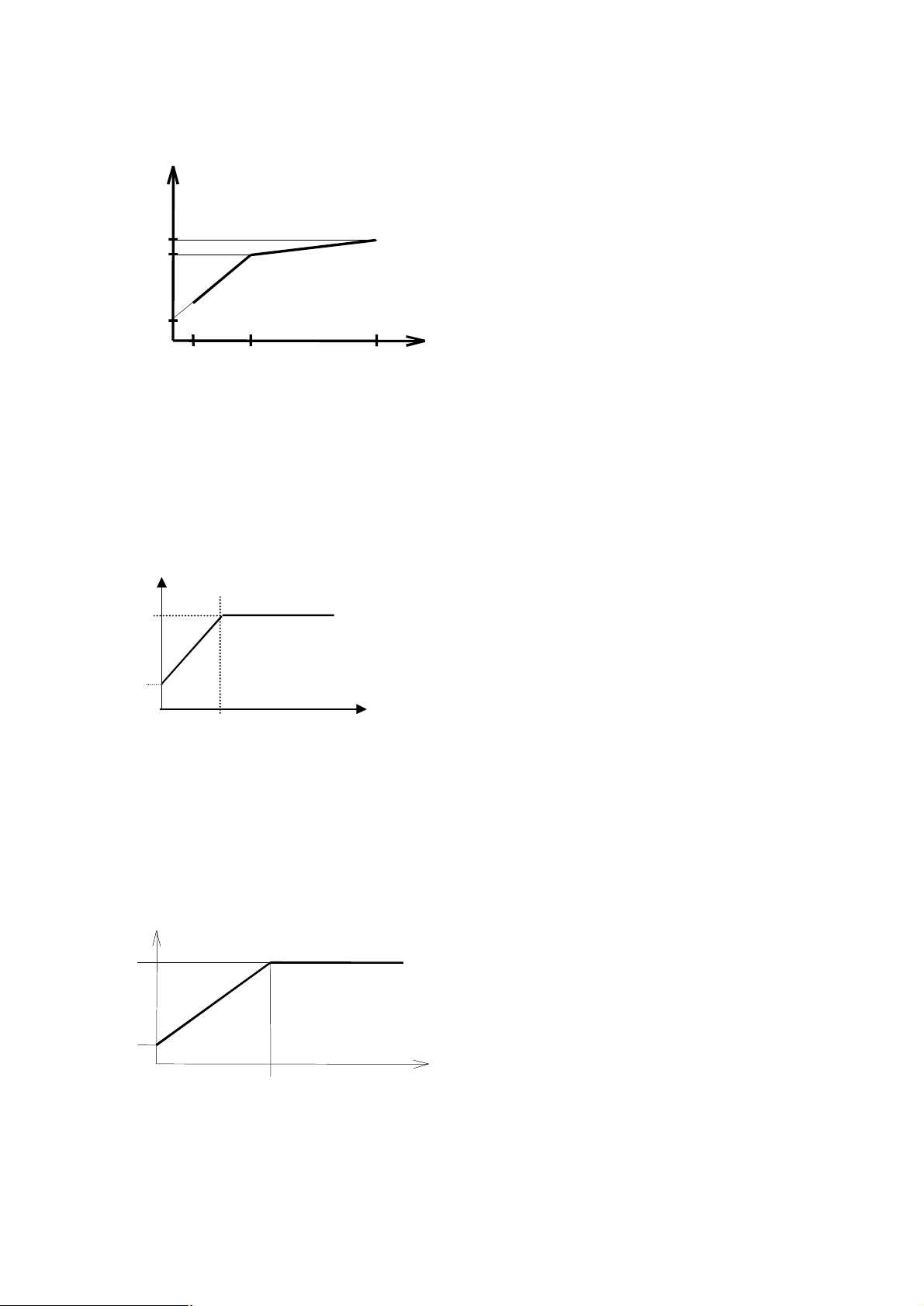
Pr.09 BOOST VOLTAGE
y
Output Frequency (Hz)
This parameter determines the minimum voltage while output frequency is low.
Pr.10 BASE_FREQUENCY (HZ)
Pr.11 BASE VOLTAGE (%)
These two parameters are determined by the motor's rated frequency and voltage.
Vout
Pr.88(%)
Pr.11(%)
Pr.09(%)
Foutput
Pr.16(Hz)
Pr.10(Hz)
Pr.15(Hz)
Pr.12 PWM_CARRIER
PDA/PDE/PDH series:
series: Defines the maximum carrier frequency. When running frequency > Pr.14, the carrier frequency will be the
value of Pr.12, otherwise it is the value of Pr.13.
PDAN series:
Pr.12 is composed of two parameters: Pr.12 = xx.y, separated by decimal point.
xx is used to define PWM CARRIER, y is used to defined CARRIER TRANSFER POINT.
MINIMUMCARRIER is fixed frequency 2KHz.
When running frequency > Transfer point , the carrier frequency will be the value xx (PWM Carrier), otherwise it is
2KHz (Minimum Carrier).
Carrier Frequency(KHz)
Pr.12=xx.y
xx
2KHz
Pr.13 PDA/PDE/PDH series: MINIMUM_CARRIER
Defines the minimum carrier frequency.
PDAN series: MODBUS Elapse time
When RS485 port is defined as MODBUS protocol, this parameter defines the maximum elapse time between two
receiving bytes.
Pr.14 PDA/PDE/PDH series: CARRIER_TRANSFER_POINT
Defines the transfer point of output frequency, when carrier frequency reaches Pr.12.
Note: Select lower carrier frequency while inverter is running at low output frequency (Hz) can decrease vibration
effect.
PWM Carrier frequency
fc(kHz)
Pr.12
Pr.13
PDAN series: Thermistor type
Defines the Thermistor type, contact factory when board changed.
Pr.15 UPPER_FREQUENCY_LIMIT
Defines maximum possible output frequency (Hz) while running. Refer to Pr.10.
Pr.16 LOWER_FREQUENCY_LIMIT
Defines minimum possible output frequency (Hz) while running. Refer to Pr.10.
Pr.14
Output frequency(Hz)
Page 20
19
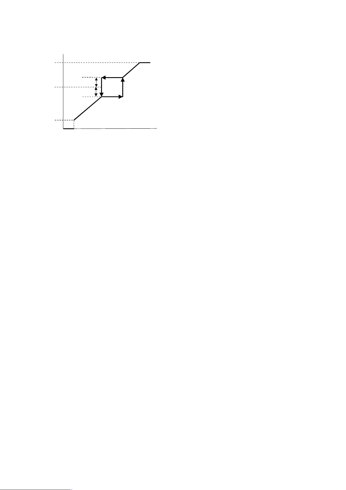
Pr.17 SKIP_FREQUENCY
Pr.18
This parameter can prevent the inverter running at the resonant point of mechanical system.
Pr.18 SKIP_BAND
This parameter defines the skip range.
HZ output
Pr.15
Pr.17
Pr.18
Pr.18
HZ desire
Pr.19 JOG SPEED (Refer to Section 8.2~8.5, 8.80~8.83 & 12)
This parameter determines the running frequency when JOG speed is required.
Pr.20 JOG ACC/DEC (Refer to 8.2~8.5, 8.84)
Defines the acceleration and deceleration rate when JOG command is in execution, or when DIx(84) is ON.
Pr.21 SPD1 SPEED SET (Refer to Section 8.2~8.5, 8.80~8.83 & 12)
This parameter determines the running frequency when SPD1 speed is required.
Pr.22 SPD1 ACC TIME (Refer to 8.2~8.5, 8.85)
Defines the acceleration rate when SPD1 command is in execution, or when DIx(85) is ON.
Pr.23 SPD1 DEC TIME (Refer to 8.2~8.5, 8.85)
Defines the deceleration rate when SPD1 command is in execution, or when DIx(85) is ON.
Pr.24 SPD2 SPEED SET (Refer to Section 8.2~8.5, 8.80~8.83 & 12)
This parameter determines the running frequency when SPD2 speed is required.
Pr.25 SPD2 ACC TIME (Refer to 8.2~8.5, 8.86)
Defines the acceleration rate when SPD2 command is in execution, or when DIx(86) is ON.
Pr.26 SPD2 DEC TIME (Refer to 8.2~8.5, 8.86)
Defines the deceleration rate when SPD2 command is in execution, or when DIx(86) is ON.
Pr.27 SPD3 SPEED SET (Refer to Section 8.2~8.5, 8.80~8.83 & 12)
This parameter determines the running frequency when SPD3 speed is required.
PDAN series: Refer to Appendix A for PID function.
Pr.28 SPD3 ACC TIME (Refer to 8.2~8.5, 8.87)
Defines the acceleration rate when SPD3 command is in execution, or when DIx(87) is ON.
PDAN series: Refer to Appendix A for PID function.
Pr.29 SPD3 DEC TIME (Refer to 8.2~8.5, 8.87)
Defines the deceleration rate when SPD3 command is in execution, or when DIx(87) is ON.
PDAN series: Refer to Appendix A for PID function.
Pr.30 FREE RUN STOP
If Pr.30 = 0, when stop, inverter gradually decreasing its output frequency and ramp down to stop. If Pr.30 = 1, when
stop, inverter disables output immediately, the motor free run.
Pr.31 REVERSE INHIBIT
If Pr.31 = 0, Inverter may run in both direction.
If Pr.31 = 1, Reverse Run is inhibited.
Pr.32 POWER FACTOR & FILTER
This parameter composed of two factors: Pr.32 = aa.bb, separated by decimal point.
aa: Rated Power Factor value from motor nameplate
bb: Filter constant for Sensor-less compensation
Pr.33 DISCHARGE_ENABLE
If Pr.33 = 0, Discharge circuit is Disabled.
If Pr.33 = 1, Discharge circuit is Enabled.
The discharge transistor will ON if the following conditions are met:
a. Inverter is Running, and
b. Inverter has no alarm, and
c. Inverter checks the VDC>117%, and
d. Only when Inverter is Deceleration.
If Pr.33 = 2, Discharge circuit is Enabled.
The discharge transistor will ON if the following conditions are met:
a. Inverter is Running, and
b. Inverter has no alarm, and
c. Inverter checks the VDC>117%
No matter the inverter is deceleration or not.
Page 21
20
Pr.34 UP/OP RESTART_ENABLE (Refer to Section 11)
q
TIME
Pr.51
150%
110%
(Irms/Pr.78)
If Pr.34 = 1, when power come back normal, the Inverter will restart automatically.
Pr.35 STALL_LEVEL
This parameter defines the current limit level (%) while STALL process.
Pr.36 BASE BLOCK TIME (Refer to Section 11)
When UP/OP occurs or DIx(8 or 18) is ON, this parameter guarantees the minimum time to disable the inverter output.
Pr.37 AM SELECT (Refer to Section 10)
Select desired variables to appear at analog output terminal.
Pr.38 AM GAIN (Refer to Section 10)
Select desired gain ratio for analog output terminal.
Pr.39 CONTROL COMMAND SELECT (Refer to Section 6)
This parameter determines the type of FWD/REV, RUN/STOP control method.
Pr.40 SPEED INPUT SELECT (Refer to Section 7)
This parameter defines the source and type for determining the running frequency.
Pr.41 DI1 FUNCTION SELECT (Refer to Section 8)
Defines the function for input terminal DI1.
Pr.42 DI2 FUNCTION SELECT (Refer to Section 8)
Defines the function for input terminal DI2.
Pr.43 DI3 FUNCTION SELECT (Refer to Section 8)
Defines the function for input terminal DI3.
Pr.44 DI4 FUNCTION SELECT (Refer to Section 8)
Defines the function for input terminal DI4.
Pr.45 DO1 FUNCTION SELECT (Refer to Section 9)
Defines the function for output terminal DO1.
Pr.46 DO2 FUNCTION SELECT (Refer to Section 9)
Defines the function for output terminal DO2.
Pr.47 RELAY FUNCTION SELECT (Refer to Section 9)
Defines the function for output RELAY terminal RY1&RY2.
Pr.48 Irms/Idc DETECTOR THRESHOLD LEVEL (Refer to Section 9.13)
This parameter is used to define the threshold level for Current Over Detector module.
Pr.49 HZ DETECTOR THRESHOLD LEVEL (Refer to Section 9.2)
Pr.50 HZ DETECTOR TOLERANCE (Refer to Section 9.2)
Pr.49 and Pr.50 are used for SPE, SPNE, SPO and SPNO output functions.
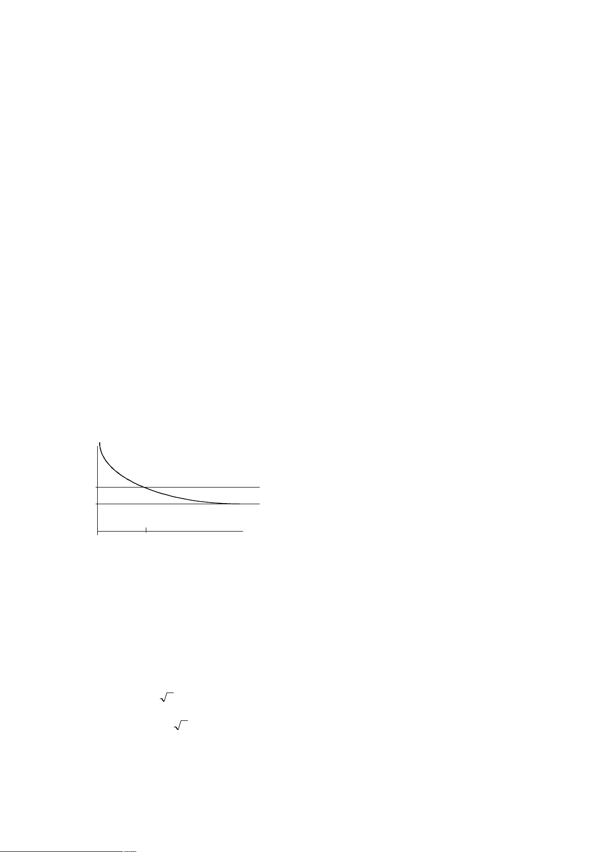
Pr.51 THERMAL TRIP TIME
This parameter defines the OVER LOAD trip time of the
INTERNAL THERMAL RELAY.
If Pr.51=0, the THERMAL RELAY function is disabled.
Pr.78 MOTOR RATING
If the inverter's rating capacity is larger than the motor in use, this
parameter can be adjusted to protect the motor.
This parameter is defined as the percentage level of the inverter
rating.
Pr.52 POLE (Refer to Section 13.1)
This parameter defines the POLE number of the motor in use.
Pr.53 GEAR_RATIO (Refer to Section 13.1)
Pole & Gear Ratio parameters will be used for RPM (Pr.58) calculation.
RPM = (120 * HZ / POLE) * GEAR_RATIO%
Pr.54 MONITOR SELECTION
More internal status or value may be monitored.
Pr.54 selects the data shown in Pr.61.
Pr.54=0: Irms (ampere)
Pr.54=1: Irms (% of inverter rating)
Pr.54=2: Irms (% of motor rating)
Pr.54=3: Power Angle q (Angle of Current Phase Lag)
Pr.54=4: Output VA=
Pr.54=5: Power Factor PF=
Pr.54=6: Watt (ac side) =
)cos(
IrmsVrms **3
)cos(***3
IrmsVrms
q
Pr.54=7: Idc (ampere) (For PDA/PDH series only)
Pr.54=8: Idc (% of inverter rating) (For PDA/PDH series only)
Pr.54=9: Watt (dc side) = Vcap*Idc (For PDA/PDH series only)
Pr.54=10: Watt (limit)
Pr.54=11: OL accumulation level
Pr.54=32: Shows timer value when it is used. (For PDAN series only)
Page 22

21
Pr.55 A/D CONVERTER CHANNEL SELECT (Refer to Section 13.3)
Pr.56 A/D CONVERSION DATA (Refer to Section 13.3)
Pr.57 HZ (Refer to Section 13.1)
Monitors the output frequency of the inverter.
Pr.58 RPM (Refer to Section 13.1)
Monitors the motor rotating speed, calculated by Pr.57 (HZ), Pr.52 (POLE), and Pr.53 (GEAR_RATIO).
RPM = ( 120 * HZ / POLE ) * GEAR_RATIO%
PDA/PDE/PDH series: Expressed in Krpm, the display shows “xx.xx” Krpm.
PDAN series: When RPM >= 10000 rpm, Expressed in Krpm, the display shows “xx.xx” Krpm,
When RPM <= 9999 rpm, Expressed in rpm, the display shows “xxxx” rpm .
Pr.59 VDC (Refer to Section 13.1)
Monitors the internal DC BUS voltage of the inverter, VDC = 1.414 * Vac (line input)
Pr.60 VOUT (Refer to Section 13.1)
Monitors the output Vrms of the inverter.
Pr.61 Irms, Idc and others (Refer to Section 13.1)
Pr.62 HEAT SINK TEMPERATURE
Monitors the temperature of internal heat sink. When the temperature exceeds 80 degree, inverter will stop and show
OH alarm.
Pr.63 Digital Input Terminal Status (Refer to Section 13.2)
Monitors the DI1~DI4 input terminal status.
Digit 3: DI1 Input Terminal Status
Digit 2: DI2 Input Terminal Status
Digit 1: DI3 Input Terminal Status
Digit 0: DI4 Input Terminal Status
Pr.64 Control Input Terminal status (Refer to Section 13.2)
Monitors the RUN & REV input terminal status.
Digit 1: RUN (or DI5) Input Terminal Status
Digit 0: REV (or DI6) Input Terminal Status
Pr.65 Digital Output Terminal status (Refer to Section 13.2)
Monitors the DO1, DO2 & RY(1,2) output terminal status.
Digit 2: DO1 Output Terminal Status
Digit 1: DO2 Output Terminal Status
Digit 0: RELAY Output Status
Pr.66 reserve
Pr.67 Operation Mode Selection
Select RUN mode as Standard V/F, Sensor-Less or Torque mode.
Refer to section4.3.
Pr.68 Sensor-Less Boost
This parameter is used under Sensor-Less mode. It will be set to suitable value during Auto-Tuning. User doesn’t have
to change it.
Refer to section4.4.
Pr.69 SLIP constant F1 / F2
Motor constant R1, R2 and L1, L2 are combined into this constant.
Refer to section4.4.
Pr.70 Analog Input Gain
Refer to Section 7.2.12, 7.2.13, 7.2.21, 7.2.22, 7.2.33, 7.2.35.
Pr.71 TIMER TIME (Refer to Section 8.7)
PDAN series: Refer to Appendix A for PID function.
Pr.72 AUTO RUN MODE SELECT (Refer to Section 12)
Pr.73 TIME PERIOD FOR AUTO RUN STEP1&6 (Refer to Section 12)
Pr.74 TIME PERIOD FOR AUTO RUN STEP2&7 (Refer to Section 12)
Pr.75 TIME PERIOD FOR AUTO RUN STEP3&8 (Refer to Section 12)
Pr.76 TIME PERIOD FOR AUTO RUN STEP4&9 (Refer to Section 12)
Pr.77 TIME PERIOD FOR AUTO RUN STEP5&10 (Refer to Section 12)
Pr.78 MOTOR RATING
Refer to the description of Pr.51.
Pr.79 RESTART TYPE SELECT (Refer to Section 11)
Pr.80 RESTART STALL LEVEL (refer to section 11)
Pr.81 SPEED SEARCH DEC TIME (Refer to Section 11)
Pr.82 VOLTAGE RECOVER TIME (Refer to Section 11)
Pr.83 IGBE GUARD TIME
This parameter defines the guard time for preventing IGBT short between upper and lower arm. Only factory can
modify this parameter. Consult factory if modification is necessary.
Page 23

22
Pr.84 INPUT SUPPLY LINE_VOLTAGE
This parameter defines the normal working voltage of the inverter.
According to this parameter, the inverter calculates all voltage dependent values.
l OP Trip Voltage (VDC) = 1.414 * Pr.84 * 130%
l UP trip Voltage (VDC) = 1.414 * Pr.84 * 70%
l OP Recover Voltage (VDC) = 1.414 * Pr.84 * 120%
l UP Recover Voltage (VDC) = 1.414 * Pr.84 * 80%
l Contactor On Voltage (VDC) = 1.414 * Pr.84 * 69%
l Contactor Off Voltage (VDC) = 1.414 * Pr.84 * 65%
Note: The "Contactor" means the device used to BY-PASS the Charging Resistor.
It may be a RELAY or a SCR instead.
There is no contactor in PDE-2007/2015
l Discharge Start Voltage (VDC) = 1.414 * Pr.84 * 117%
Note: there is no internal discharge transistor in PDE-2007/15
Pr.85 INVERTER RATED CURRENT
This parameter defines the rated output current of the inverter.
Pr.86 IRMS ADJUST
This parameter is used to adjust the IRMS data reading.
Pr.87 VDC ADJUST
This parameter is used to adjust the VDC data reading (Refer to Section 13.1).
Pr.88 MAXIMUM OUTPUT VOLTAGE (%)
The parameter determines maximum output voltage when running at maximum frequency. Refer to description of Pr.10,
Pr.11 and Pr.15.
Pr.89 AI1_LOW
This parameter is used to record the A/D converter data when "AI1" input terminal is connected to "ACOM" terminal.
(JP1 select +5V)
Pr.90 AI1_HIGH
This parameter is used to record the A/D converter data when "AI1" input terminal is connected to "+5V" voltage
source. (JP1 select +5V)
Pr.91 AI2_LOW
This parameter is used to record the A/D converter data when "AI2" input terminal is connected to "ACOM" terminal.
(JP2 select +5V) Note: this parameter also used by AI3.
Pr.92 AI2_HIGH
This parameter is used to record the A/D converter data when "AI2" input terminal is connected to "+5V" terminal. (JP2
select +5V) Note: this parameter also used by AI3.
Pr.93 UNIT_NUMBER & BAUD_RATE (only for communication option card)
While using serial communication control, this parameter is used to define the BAUD RATE, PROTOCOL and UNIT
NUMBER (or station address).
Refer to section 15
Pr.94 PARAMETER RELOAD (Refer to Section 5.3)
Pr.95 MEMORY PROTECT (Refer to Section 5.2)
Pr.96 FACTORY WRITE ENABLE (Refer to Section 5.2)
Pr.97 VERSION
This parameter indicates the software revision of this inverter.
Pr.98 MONITOR (I) (Refer to Section 13)
Pr.99 MONITOR (HZ) (Refer to Section 13)
By changing Pr.98 and Pr.99, user can select any two variables for frequent monitoring.
Note: For PDE series, Pr.61 (Irms) always shows 0.0 ampere. User can monitor other important variable by changing
this parameter.
Page 24
23
6. Selection of RUN/STOP/FWD/REV control command
Before start running the inverter, the most important step is to select the Control Command Source. You can choose
whether the control command will come from panel or terminal.
If the control command should come from terminal, then the two input terminals RUN and REV are used for controlling the
inverter.
These two input terminals are OFF when left open and will be ON when connected to DCOM terminal.
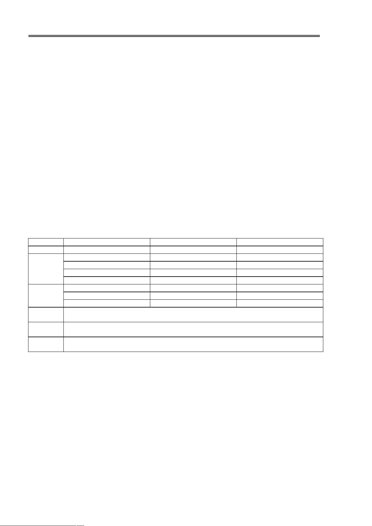
Parameter Pr.39 is used to select the source of Control Command.
CMD_SELECT Pr.39 = a. b, is composed of two selections "a" and "b" in one parameter,
If DIx(89) or DIx(90) is ON, then CMD_SELECT="b", else CMD_SELECT="a".
Refer to DIx(89) and DIx(90).
If CMD_SELECT=0
The RUN and REV terminals are disabled.
Control Command will come from the keypad panel.
Push FWD key, the inverter will run forward direction.
Push REV key, the inverter will run forward direction.
If CMD_SELECT=1
The RUN terminal will start the inverter running, and REV terminal controls the
running direction.
If CMD_SELECT=2
The RUN terminal is equivalent to FORWARD-RUN.
The REV terminal is equivalent to REVERSE-RUN.
If CMD_SELECT=3
Similar to mode-1, but will check RUN terminal at OFF position while power on.
If CMD_SELECT=4
Similar to mode-2, but will check RUN & REV at OFF position while power on.
If CMD_SELECT=5 (for PDAN series only)
When RS485 port is defined as JPS protocol, RUN/STOP command comes from RS485 Serial Port.
Note: Refer to Sec.7 concerning how to determine the running frequency.
Pr.39 "RUN" Terminal "REV" Terminal FUNCTION
0 Don’t care Don’t care Command from PANEL
OFF Don’t care STOP
1
2
3
4
5
Similar to Mode-1, When after RESET, if RUN terminal is not in OFF position, the inverter will
show "--on”, warning the user to remove the control signal.
Similar to Mode-2, When after RESET, if RUN and REV terminals are not in OFF position, the
inverter will show "--on”, warning the user to remove the control signals.
When RS485 port is defined as JPS protocol, RUN/STOP command comes from RS485 Serial Port.
(For PDAN series using JPS protocol only)
OFF Don’t care STOP
ON OFF FORWARD RUN
ON ON REVERSE RUN
OFF OFF STOP
OFF ON REVERSE RUN
ON Don’t care FORWARD RUN
Page 25
24
7. Selection of Set Frequency
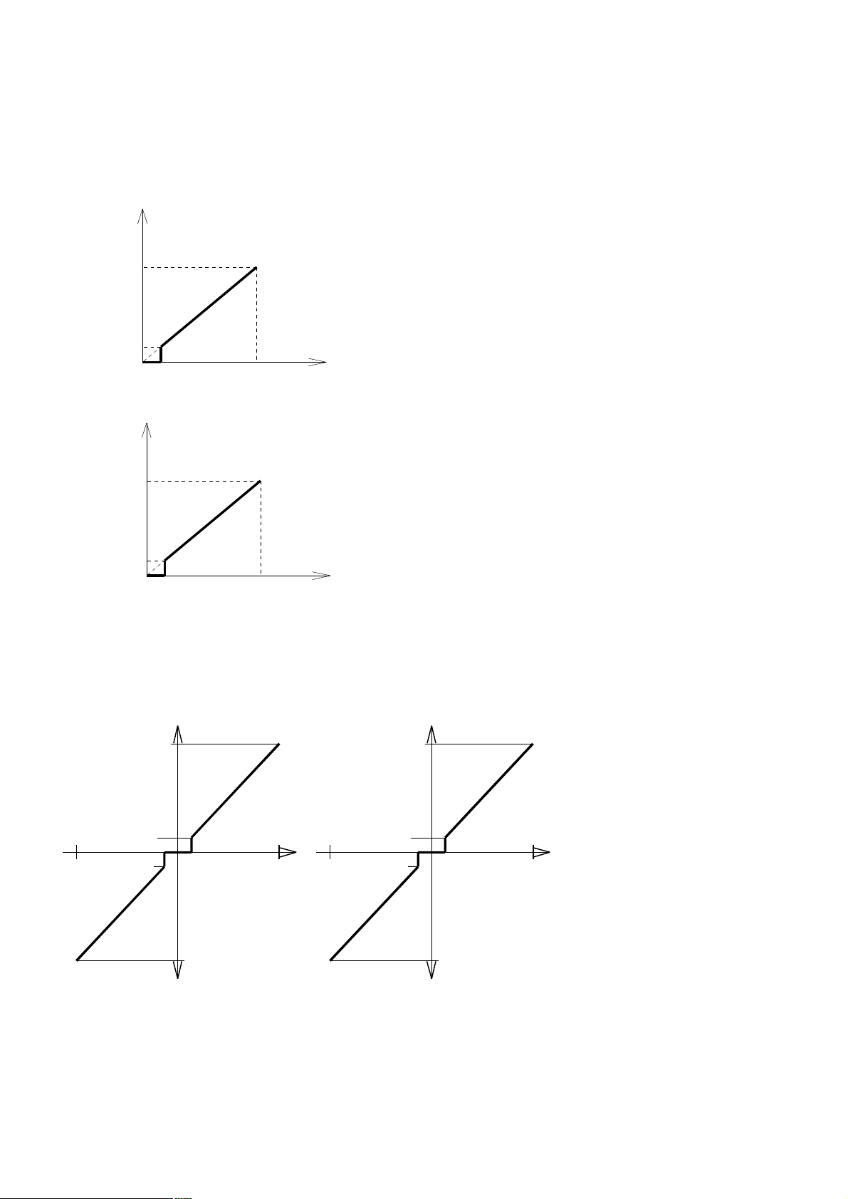
SPEED_SELECT parameter Pr.40 is used for speed input source selection. Through setting Pr.40, the speed input sources
may come from Panel, Memory, Analog input, Up/Down counter, or the combinations of the above sources.
Note that, Pr.40 = cc. dd, is composed of two selections "cc" and "dd" in one parameter. If DIx(88) or DIx(90) is ON,
then SPEED_SELECT="dd", else SPEED_SELECT="cc". Refer to DIx(88) and DIx(90).
7.1 Set Frequency Source Selection Table
Pr.40 SPEED source DIRECTION Source
0 Set value in Pr.00 Refer to Sec.6
1 AI1 Refer to Sec.6
2 AI2 Refer to Sec.6
3 Set value from Panel Refer to Sec.6
4 Both the output frequency and direction determined by AI1
5 Both the output frequency and direction determined by AI2
6 By internal U/D counter Refer to Sec.6
7 Similar to Pr.40=6, but will preload U/D counter from Pr.00 after RESET.
8 Similar to Pr.40=3, with PRELOAD from & AUTO WRITE to Pr.00
9 Similar to Pr.40=4, but will not STOP while desired frequency is lower then Pr.16 (low limit)
10 Similar to Pr.40=5, but will not STOP while desired frequency is low then Pr.16 (low limit)
11 Same as Pr.40=6.
12
13
14 Reserve
15 Reserve
16 Reserve
17 Similar to Pr.40=1, With Minimum = Pr.16 (low limit)
18 Similar to Pr.40=2, With Minimum = Pr.16 (low limit)
19 Similar to Pr.40=11, With Auto Reload from and Auto Write to Pr.00
20 Reverse to Pr.40=18, +5V(or 20mA)---> Lower Limit, 0V---> Upper Limit Frequency
21
22
23~24 Reserve
25 AI3 used as frequency source (similar to mode 2)
26 AI3 used as bi-directional frequency source (similar to mode 5)
27 AI3 as bi-directional frequency source with minimum speed (similar to mode 10)
28
29
30 AI3 as input, with minimum speed (Similar to Pr.40=18)
31 AI3 as input with reverse slope (similar to mode 20)
32 AI1 as input with reverse slope (similar to mode 20)
33
34
35
36
37 AI1 FORWARD, AI2 REVERSE
38 AI2 FORWARD, AI1 REVERSE
39 Similar to Pr.00, but runs at Pr.16 when Pr.00<Pr.16
40 Output frequency determined by PID Output
41~45 Reserve
46 Speed Command come from RS485 Serial Port (for PDAN series using JPS protocol only)
47 Reserve
48 Set Frequency = PID Boost * (PID Output + PID Bias Input from AI1)
49 Set Frequency = PID Boost * (PID Output + PID Bias Input from AI2)
50 Set Frequency = PID Boost * (PID Output + PID Bias Input from AI3)
51 Set Frequency = PID Boost * (PID Output + PID Bias Set by Pr.028)
JP1 is used for changing the configuration of analog input AI1 (refer to Sec.1.2.1.a).
It may select 0~+5V(default) or 0~+10V.
JP2 is used for changing the configuration of analog input AI2 (refer to Sec.1.2.1.b).
It may select 0~+5V(default) or 0~20mA.
JP3 is used for changing the source of AI3 (refer to Sec.1.2.1.c)
Set Frequency = AI1 * ( 100%± (Pr.70*AI2) ), With Minimum =Pr.16 (low limit)
Set Frequency = AI2± ( Pr.15 * (Pr.70*AI1) ), With Minimum = Pr.16 (low limit)
Frequency Set = Panel(Computer) Set * ( 100%± (Pr.70*AI2) )
Set Frequency = Panel(Computer) Set± ( Pr.15 * (Pr.70*AI1) ), With Minimum = Pr.16
Set Frequency = AI1 * ( 100%± (Pr.70*AI3) ), With Minimum =Pr.16 (similar to mode12)
Set Frequency = AI3± ( Pr.15 * (Pr.70*AI1) ), With Minimum = Pr.16 (similar to mode13)
Set Frequency = Panel(Computer) Set * ( 100%± (Pr.70*AI1) )
Set Frequency = Panel(Computer) Set * ( 100%± (Pr.70*AI3) )
Set Frequency = Panel(Computer) Set± ( Pr.15 * (Pr.70*AI2) ), With Minimum = Pr.16
Set Frequency = Panel(Computer) Set± ( Pr.15 * (Pr.70*AI3) ), With Minimum = Pr.16
Page 26
25
7.2 Description of Frequency Input Sources
0V
0V
7.2.0 Pr.40 = 0, Speed input come from Pr.00
Parameter Pr.00 is the MAIN_SPEED_SET parameter stored in EAROM memory.
The value once written into Pr.00 will never be altered, unless you re-write a new value again.
In this mode, the Hz value stored in Pr.00 will be used to determine the output frequency of the inverter while running.
The direction of the output phase sequence must be determined by control command.
Note: Changing the content in Pr.00 will immediately change the output frequency even if the inverter is running.
7.2.1 Pr.40 = 1, Speed input come from AI1
Hz
Pr.15
Pr.16
0 +5V(or +10V)
7.2.2 Pr.40 = 2, Speed input come from AI2
Hz
Pr.15
Pr.16
0 +5V(or 20mA)
7.2.3 Pr.40 = 3, Speed input come from Key-pad setting
The set frequency comes from keypad directly.
Or if communication option is used, set frequency comes from communication command.
The direction of the output phase sequence must be determined by control command.
Note: When start running; the minimum running frequency shall be Pr.16.
7.2.4 Pr.40 = 4, Speed input come from AI1 with Bi-direction control
Hz (forward)
Pr.15
Pr.16
Pr.16
2.5V
+5V
Pr.15
Hz (reverse)
JP1 set to +5V
In this mode, the voltage signal fed into AI1 terminal will be used to
determine the output frequency of the inverter while running.
The direction of the output phase sequence must be determined by
control command.
If the input signal reaches maximum level, the set frequency is equal to
Pr.15 (UPPER LIMIT).
If the desired set frequency is lower than Pr.16 (LOWER LIMIT), the
inverter will stop.
Note:
Set jumper JP1 to match the input voltage range.
Vin
If necessary, use Pr.89 & Pr.90 to modify the input range.
In this mode, the voltage signal fed into AI2 terminal will be used to
determine the output frequency of the inverter while running.
The direction of the output phase sequence must be determined by
control command.
If the input signal reaches maximum level, the set frequency is equal
to Pr.15 (UPPER LIMIT).
If the desired set frequency is lower than Pr.16 (LOWER LIMIT), the
inverter will stop.
Note:
Set jumper JP2 to match the input signal type and range. If
Vin
necessary, use Pr.91 & Pr.92 to modify the input range.
Hz (forward)
Pr.15
In this mode, the voltage signal fed
into AI1 terminal will be used to
determine the output frequency and
direction of the inverter.
The input signal level determines the
direction of the output phase
sequence.
If the input signal is maximum level,
Pr.16
the set frequency is equal to Pr.15
(UPPER LIMIT) in forward
Pr.16
5V
+10V
direction; and if the input signal is
zero, the set frequency is equal to
Pr.15 in reverse direction.
If the input is around half level, the
inverter will stop.
Pr.15
Hz (reverse)
JP1 set to +10V
Note: Set jumper JP1 to match the
input voltage range. If necessary,
use Pr.89 and Pr.90 to modify the
input range.
Page 27
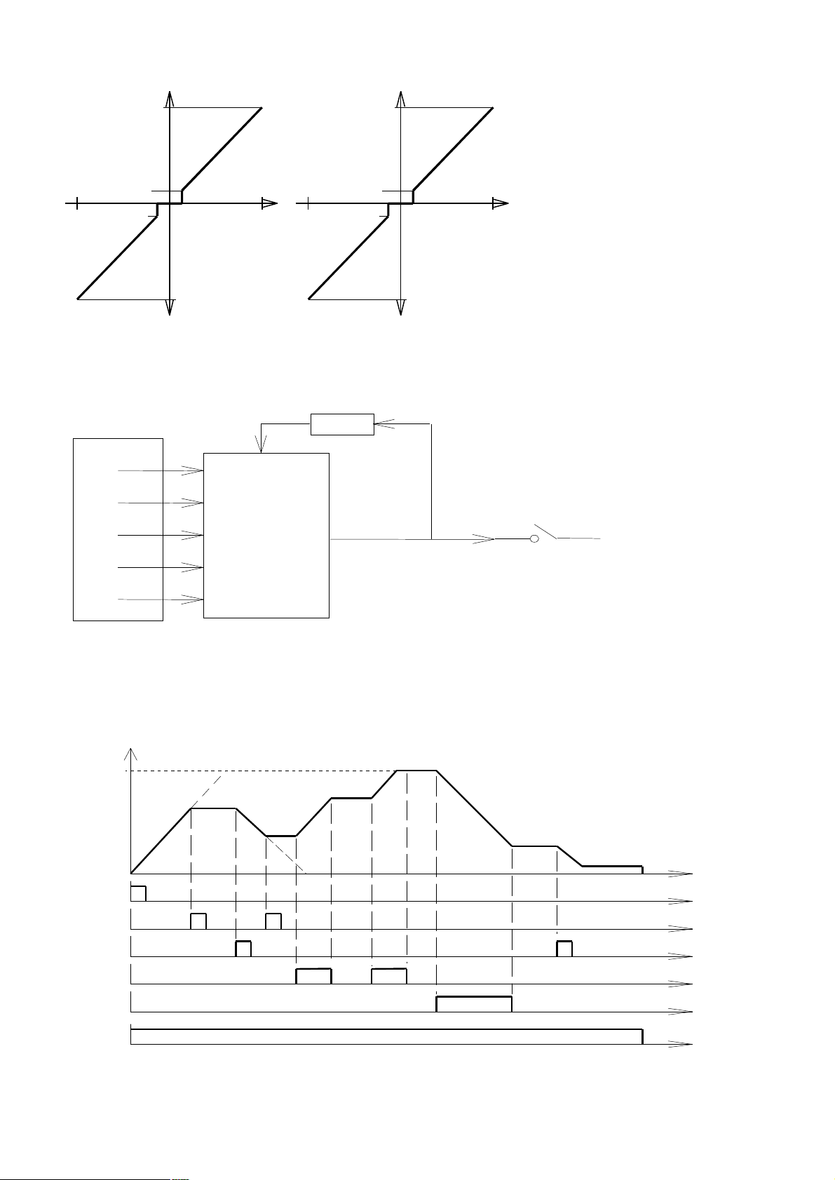
26
7.2.5 Pr.40 = 5, Speed input come from AI2 with Bi-direction control
*3
0V
0V
Hz (forward)
Pr.15
Hz (forward)
Pr.15
In this mode, the voltage signal fed into
AI2 terminal will be used to determine the
output frequency and direction of the
inverter.
The input signal level determines the
direction of the output phase sequence.
Pr.16
Pr.16
If the input signal is positive maximum
level, the set frequency is equal to Pr.15
Pr.16
2.5V
+5V
Pr.16
10mA
20mA
(UPPER LIMIT) in forward direction; and
if the input signal is zero, the set frequency
is equal to Pr.15 in reverse direction.
If the input is around half level, the
inverter will stop.
Pr.15
Hz (reverse)
JP2 set to +5V
JP2 set to 20mA
Pr.15
Hz (reverse)
Note: Set jumper JP2 to match with the
input signal type and range. If necessary,
use Pr.91 and Pr.92 to modify the input
range.
7.2.6 Pr.40 = 6, Speed input come from Internal Up/Down Counter
7.2.7 Pr.40 = 7, Speed input come from Internal Up/Down Counter with Preload from Pr.00
Note: When start running; the minimum running frequency shall be Pr.16.
*2
*4
Pr.00
UP
Preload
DOWN
LOAD
CLEAR
*1
Counter output
Pr.40=6,7,11 or 19
Hz desire
Internal
HOLD
Up/Down
Counter
Functional Block Diagram of the Internal UP/DOWN Counter
*1. If Pr.40=6, 7, 11, or 19, the counter output is used to determine the output frequency.
*2. If Pr.40=7 or 19, Data in Pr.00 will preload into the counter when Power On or after Reset.
*3. If Pr.40=19, after Up/Down execution, the content of counter will write into Pr.00 automatically.
*4. These signals come from Digital Input (DIx) terminal. Refer to Sec.8 for detail description.
Hz(using Up/Down Module)
Pr.15
Pr.16
LOAD
HOLD
CLEAR
UP
DOWN
RUN
UP/DOWN COUNTER OPERATION EXAMPLE
Page 28
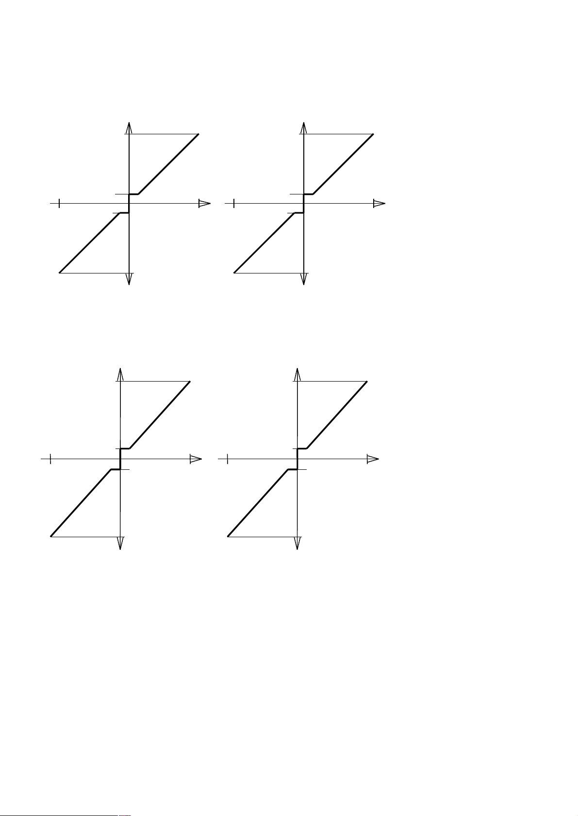
27
7.2.8 Pr.40 = 8, Similar to mode 3, with Preload from Pr.00 (and Auto Write to Pr.00)
JP1 set to +5V
JP1 set to +10V
0V
0V
JP2 set to +5V
JP2 set to 20mA
This function is similar to Pr.40=3, with only two differences:
a. When Power On or after Reset, the data in Pr.00 will preload into set frequency buffer.
b. When using LOCAL panel, after changing ser frequency, the buffer value will write back into Pr.00 automatically.
Note: When start running; the minimum running frequency shall be Pr.16.
7.2.9 Pr.40 = 9, Similar to mode 4, with minimum running speed
7.2.10 Pr.40 = 10, Similar to mode 5, with minimum running speed
7.2.11 Pr.40 = 11, Same as mode 6
7.2.12 Pr.40 = 12 , Speed input is the combination of AI1 * ( 100%± (Pr.70*AI2) )
In this mode, the desired set frequency is the combination of AI1 and AI2.
Set Frequency = AI1 * ( 100%± (Pr.70*AI2) )
Analog signal from AI1 is selected to be the master set frequency; and signal from AI2 is the proportional rate input.
If signal level of AI2 is maximum, the modification rate equal (100%+Pr.70);
and if AI2 is minimum, the modification rate is (100%-Pr.70).
Note: Minimum-running frequency is Pr.16.
Typical application is as follows:
Hz (forward)
Pr.15
Pr.16
Pr.16
Hz (reverse)
Hz (forward)
Pr.15
Pr.16
Hz (reverse)
2.5V
Pr.15
Pr.16
Pr.15
+5V
+5V
Hz (forward)
Pr.15
Pr.16
Pr.16
Hz (reverse)
Hz (forward)
Pr.15
Pr.16
Hz (reverse)
5V
Pr.15
Pr.16
Pr.15
+10V
+20mA
In this mode, the voltage signal fed
into AI1 terminal will be used to
determine the output frequency and
direction of the inverter.
The input signal level determines
the direction of the output phase
sequence.
If the input signal is maximum
level, the set frequency is equal to
Pr.15 (UPPER LIMIT) in forward
direction, and if the input signal is
zero, the set frequency is equal to
Pr.15 in reverse direction.
If the input is around half level, the
inverter will run at Pr.16 (LOWER
LIMIT).
Note: Set jumper JP1 to match
with the input voltage range. If
necessary, use Pr.89 and Pr.90 to
modify the input range.
In this mode, the voltage signal fed
into AI2 terminal will be used to
determine the output frequency and
direction of the inverter.
The input signal level determines
the direction of the output phase
sequence.
If the input signal is positive
maximum level, the set frequency
is equal to Pr.15 (UPPER LIMIT)
in forward direction; and if the
input signal is zero, the set
frequency is equal to Pr.15 in
reverse direction.
If the input is around half level, the
inverter will run at Pr.16 (LOWER
LIMIT).
Note: Set jumper JP2 to match
with the input signal type and
range. If necessary, use Pr.91
and Pr.92 to modify the input
range.
Page 29
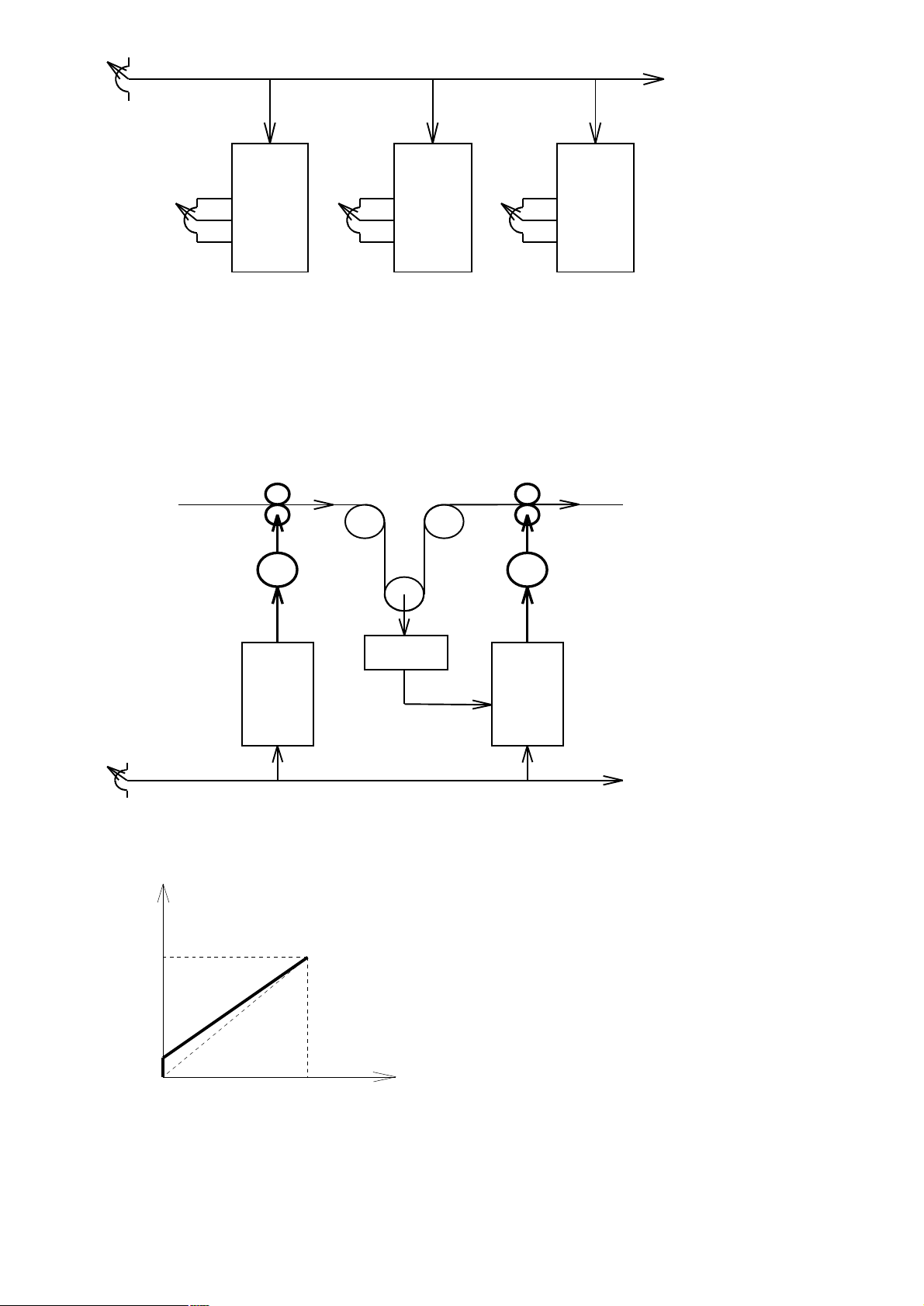
28
Master Speed Set
To other inverters
AI1
Rate 1Rate 2Rate 3
+5V
AI2
ACOM
INV1
AI1
+5V
AI2
ACOM
INV2
AI1
+5V
AI2
ACOM
INV3
7.2.13 Pr.40 = 13 , Speed input is the combination of AI2± ( Pr.15 * (Pr.70*AI1) )
In this mode, the desired set frequency is the combination of AI1 and AI2.
Set Frequency = AI2± ( Pr.15 * (Pr.70*AI1) )
Analog signal from AI2 is selected to be the major set frequency; and signal from AI1 is the auxiliary input.
If signal level of AI1 is maximum, the modification quantity is (Pr.15 * Pr.70);
and if AI1 is minimum, the modification quantity is -(Pr.15 * Pr.70).
Note: Minimum-running frequency is Pr.16.
Typical application is as follows:
M1 M2
INV1
AI2
Master Speed Set
Position
Detector
INV2
AI1
AI2
7.2.14 Pr.40 = 14 ~ 16, Reserved for factory use
7.2.17 Pr.40 = 17, Similar to mode 1, with minimum frequency = Pr.16
Hz
While the desired output frequency is lower than Pr.16
(LOWER LIMIT), the actual output frequency will maintain at
the lower frequency limit.
Note:
Pr.15
Set jumper JP1 to match with the input voltage range. If
necessary, use Pr.89 and Pr.90 to modify the input range.
Vin
Pr.16
0 +5V(or +10V)
To other inverters
Page 30
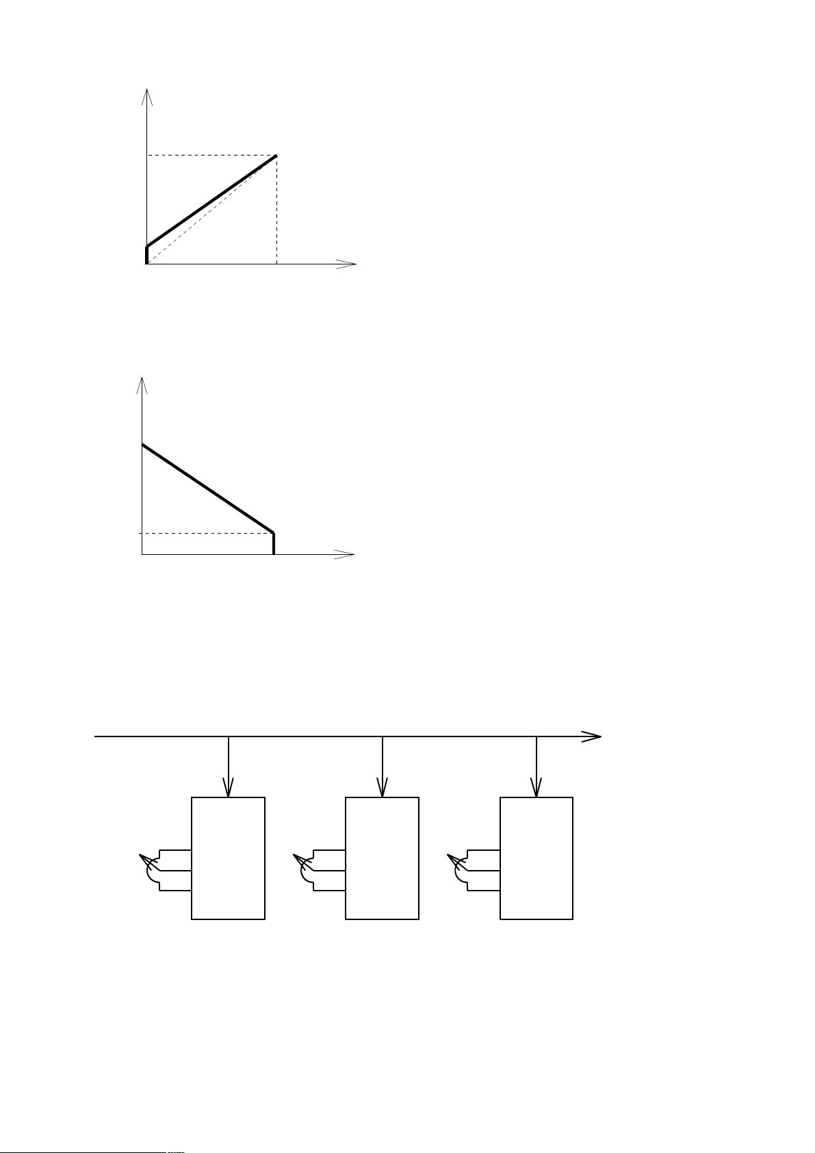
29
7.2.18 Pr.40 = 18, Similar to mode 2, with minimum frequency = Pr.16
Hz
Pr.15
Pr.16
0 +5V(or 20mA)
7.2.19 Pr.40 = 19, Similar to mode 11, with Preload and Auto Write
Refer to Sec.7.2.6, Sec.7.2.7.
7.2.20 Pr.40 = 20, Similar to mode 18, with Reverse Slope
Hz
Pr.15
Pr.16
0 +5V( or 20mA)
7.2.21 Pr.40=21, Set frequency = Panel set frequency * ( 100%± (Pr.70*AI2) )
This mode is similar to mode-12; however, Panel-Set Frequency is used instead of AI1 input.
In this mode, the desired set frequency is the combination of Panel input and AI2.
Set Frequency = Panel-Set * ( 100%± (Pr.70*AI2) )
If signal level of AI2 is maximum, the modification rate equal (100%+Pr.70);
and if AI2 is minimum, the modification rate is (100%-Pr.70).
Note: Minimum-running frequency is Pr.16.
This function is useful when master computer controls multiple inverters.
Master Speed Set by KEY-PAD Panel or Computer(from serial port)
While the desired output frequency is lower than Pr.16
(LOWER LIMIT), the actual output frequency will maintain at
the lower frequency limit.
Note:
Set jumper JP2 to match with the input signal type and
range. If necessary, use Pr.91 and Pr.92 to modify the
input range.
Vin
In this mode, the voltage signal fed into AI2 terminal will be
used to determine the output frequency of the inverter while
running.
The direction of the output phase sequence must be determined
by control command.
If the input signal reaches maximum level, the set frequency is
equal to Pr.16 (LOWER LIMIT).
On the contrary, if the input signal is zero, the set frequency is
equal to Pr.15 (UPPER LIMIT).
Note:
Set jumper JP2 to match with the input signal type and
range. If necessary, use Pr.91 and Pr.92 to modify the
Vin
input range.
Rate 1Rate 2Rate 3
+5V
AI2
ACOM
INV1
+5V
AI2
ACOM
INV2
+5V
AI2
ACOM
INV3
To other inverters
Page 31
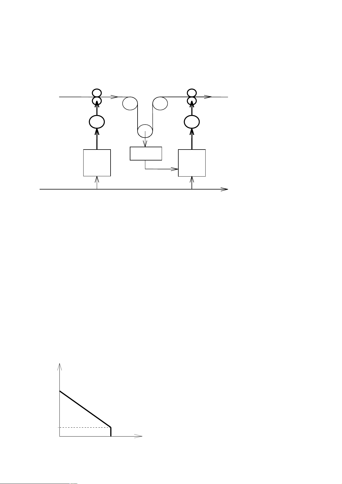
30
7.2.22 Pr.40=22, Set frequency = Panel set frequency± ( Pr.15 * (Pr.70*AI1) )
Detector
AI1
To other
M1
M2
This mode is similar to mode-13; however, Panel-Set Frequency is used instead of AI2 input.
In this mode, the desired set frequency is the combination of Panel input and AI1.
Set Frequency = Panel-Set ± ( Pr.15 * (Pr.70*AI1) )
Frequency command for Panel (or computer) is selected to be the major set frequency; and signal from AI1 is the
auxiliary input.
If signal level of AI1 is maximum, the modification quantity is (Pr.15 * Pr.70);
And if AI1 is minimum, the modification quantity is -(Pr.15 * Pr.70).
Note: Minimum-running frequency is Pr.16.
This function is useful when master computer controls multiple inverters.
INV1
Master Speed Set by KEY-PAD Panel or Computer(from serial port)
Position
INV2
7.2.23 Pr.40=23~24, reserve
7.2.25 Pr.40=25, AI3 use as frequency source (Similar to mode 2)
This mode is similar to mode2, but AI3 is used instead of AI2. Pr.91 and Pr.92 are used to define the high and low limit
of AI3. Input range is 0~+5V.
7.2.26 Pr.40=26, AI3 used as bi-directional frequency source (Similar to mode 5)
This mode is similar to mode5, but AI3 is used instead of AI2. Pr.91 and Pr.92 are used to define the high and low limit
of AI3. Input range is 0~+5V.
7.2.27 Pr.40=27, AI3 used as bi-directional frequency source with minimum speed
This mode is similar to mode10, but AI3 is used instead of AI2. Pr.91 and Pr.92 are used to define the high and low
limit of AI3. Input range is 0~+5V.
7.2.28 Pr.40=28 , Speed input is the combination of AI1 * ( 100% ± (Pr.70*AI3) )
This mode is similar to mode12, but AI3 is used instead of AI2. Pr.91 and Pr.92 are used to define the high and low
limit of AI3. Input range is 0~+5V.
7.2.29 Pr.40=29 , Speed input is the combination of AI3 ± ( Pr.15 * (Pr.70*AI1) )
This mode is similar to mode13, but AI3 is used instead of AI2. Pr.91 and Pr.92 are used to define the high and low
limit of AI3. Input range is 0~+5V.
7.2.30 Pr.40=30, Use AI3 as speed source, with minimum frequency = Pr.16
This mode is similar to mode18, but AI3 is used instead of AI2. Pr.91 and Pr.92 are used to define the high and low
limit of AI3. Input range is 0~+5V.
7.2.31 Pr.40=31, AI3 input, with Reverse Slope
This mode is similar to mode20, but AI3 is used instead of AI2. Pr.91 and Pr.92 are used to define the high and low
limit of AI3. Input range is 0~+5V.
7.2.32 Pr.40=32, AI1 input, with Reverse Slope
Hz
This mode is similar to mode20, but AI1 is used instead of AI2. In
this mode, the voltage signal fed into AI1 terminal will be used to
determine the output frequency of the inverter while running.
The direction of the output phase sequence must be determined by
control command.
Pr.15
If the input signal reaches maximum level, the set frequency is
equal to Pr.16 (LOWER LIMIT).
On the contrary, if the input signal is zero, the set frequency is
equal to Pr.15 (UPPER LIMIT).
Note: Set jumper JP1 to match with the input signal type and
Pr.16
range. If necessary, use Pr.89 and Pr.90 to modify the input
range.
Vin
0 +5V( or +10V)
Page 32

31
7.2.33 Pr.40=33, Set frequency = Panel set frequency * ( 100% ± (Pr.70*AI1) )
This function is similar to mode 21, but the modification input is AI1.
7.2.34 Pr.40=34, Set frequency = Panel set frequency * ( 100% ± (Pr.70*AI3) )
This function is similar to mode 21, but the modification input is AI3.
7.2.35 Pr.40=35, Set frequency = Panel set frequency± ( Pr.15 * (Pr.70*AI2) )
This function is similar to mode 22, but the modification input is AI2.
7.2.36 Pr.40=36, Set frequency = Panel set frequency± ( Pr.15 * (Pr.70*AI3) )
This function is similar to mode 22, but the modification input is AI3.
7.2.37 Pr.40=37, AI1 FORWARD, AI2 REVERSE
While motor run in FORWARD direction, it is same as mode 17, use AI1 as input source.
If the motor run in REVERSE direction, it is same as mode 18, use AI2 as input source.
7.2.38 Pr.40=38, AI2 FORWARD, AI1 REVERSE
While motor run in FORWARD direction, it is same as mode 18, use AI2 as input source.
If the motor run in REVERSE direction, it is same as mode 17, use AI1 as input source.
7.2.39 Pr.40=39, When start running, the output frequency is determined by Pr.00.
If in the case when Pr.00<Pr.16, the inverter will output the frequency stored in Pr.16.
7.2.39 Pr.40=40, The output frequency is determined PID Output. (for PDAN series only)
Refer to Appendix A.
7.2.41 Pr.40=41~45, reserve
7.2.46 Pr.40=46, Speed Command come from RS485 Serial Port (for PDAN series only)
When RS485 port is defined as JPS protocol, Speed Command come from RS485 Serial Port.
7.2.47 Pr.40=47, reserve
7.2.48 Pr.40=48, Set Frequency = PID Boost * (PID Output + PID Bias Input from AI1) (for PDAN series only)
7.2.49 Pr.40=49, Set Frequency = PID Boost * (PID Output + PID Bias Input from AI2) (for PDAN series only)
7.2.50 Pr.40=50, Set Frequency = PID Boost * (PID Output + PID Bias Input from AI3) (for PDAN series only)
7.2.51 Pr.40=51, Set Frequency = PID Boost * (PID Output + PID Bias Set by Pr.28) (for PDAN series only)
Refer to Appendix A.
Page 33
32
8. Selection of Digital input function
Pr.41,42,43,44
FUNCTION
COMMENT
0
NULL
NO FUNCTION
1
EMS
EMERGENCY STOP
2
SPD3
SPEED SET
3
SPD2
SPEED SET
4
SPD1
SPEED SET
5
JOG
JOG SPEED SET
6
OH
OVER HEAT ERROR,
7
TMIA
TIMER INPUT for TYPE A
8
ON_BB
BASE BLOCK if DIx is ON
9
FJR
FORWARD JOG RUN
10
RJR
REVERSE JOG RUN
11
TMIB
TIMER INPUT for TYPE B
12~14
Reserve 15
U/D COUNTER CLEAR
SET UP/DOWN COUNTER to Pr.16
16
U/D COUNTER LOAD
SET UP/DOWN COUNTER to Pr.15
17
U/D COUNTER HOLD
HOLD "Output HZ" to UP/DOWN COUNTER
18
OFF_BB
BASE BLOCK if DIx is OFF
19
U/D COUNTER UP
INCREASE UP/DOWN COUNTER
20
U/D COUNTER DOWN
DECREASE UP/DOWN COUNTER
21
ALARM CLEAR
CLEAR ALARM WHEN ALARM OCCUR
22
SET1 (FF1)
SET input of Flip/Flop-1
23
CLR1 (FF1)
CLEAR input of Flip/Flop-1
24
SET2 (FF2)
SET input of Flip/Flop-2
25
CLR2 (FF2)
CLEAR input of Flip/Flop-2
26
SET (FF1&FF2)
SET input to both FF1 & FF2
27
CLR (FF1&FF2)
CLEAR input to both FF1& FF2
28
CLK Input
Input CLOCK to Timer/Counter Block
29
Reserve 30
/OH
OVER HEAT ERROR, (input open)
31
Normal/Auto SW
Change Over Switch for Normal or Auto Run
32~35
Reserve 36
TMIC
TIMER INPUT for TYPE C
37~47
Reserve 48
Speed Hold
Hold Output Speed
49
Reserve 50
PID Enable
PID Enable
51
PID Hold
PID Integrator Hold
52
PID Clear
PID Integrator Clear
53
PID Preset
Preset PID Integrator
54
PID Bias Enable
PID Bias Enable
55
PID Boost Enable
PID Boost Enable
56-68
Reserve 69
DC-BRAKE1
DC injection brake use AI1 as brake level
70
DC-BRAKE2
DC injection brake use AI2 as brake level
71
DC-BRAKE3
DC injection brake use AI3 as brake level
72
Sensor-Less Mode Change
Select or non-select the SENSOR-LESS mode
73
RUN function
Select standard RUN function, Refer to Sec.6
74
REV function
Select standard REV function, Refer to Sec.6
75
POWER-CONTROL select
Select AI2 or AI3 for Power Control input
76
FORWARD INHIBIT
Forward run inhibit
The terminals DI1, DI2, DI3, & DI4 are multi-functioned Digital Input terminals.
【Note】All the DIx terminals are scanned once every 5.0 ms.
These four terminals are exactly identical in its hardware/software configurations.
When left open, they are OFF. And will become ON when connected to DCOM.
Each input terminal can be configured individually by corresponding DIx_SELECT parameters.
The four DIx_SELECT parameters are:
Pr.41 -- DI1_SELECT, used for DI1
Pr.42 -- DI2_SELECT, used for DI2
Pr.43 -- DI3_SELECT, used for DI3
Pr.44 -- DI4_SELECT, used for DI4
Pr.03 -- DI5_SELECT, used for DI5 (Sec. 1.2 RUN mark terminal)
Pr.04 -- DI6_SELECT, used for DI6 (Sec. 1.2 REV mark terminal)
Selection Table of Digital input function
Page 34
33
Pr.41,42,43,44
FUNCTION
COMMENT
77
REVERSE INHIBIT
Reverse run inhibit
78
PANEL FREQUENCY UP
INCREASE PANEL FREQUENCY when Pr.40=8
79
PANEL FREQUENCY DOWN
DECREASE PANEL FREQUENCY when Pr.40=8
80
SPEED SW 1
81
SPEED SW 2
82
SPEED SW 3
83
SPEED SW 4
16 SPEED SELECT
84
JOG ACC/DEC TIME
85
SPD1 ACC/DEC TIME
86
SPD2 ACC/DEC TIME
87
SPD3 ACC/DEC TIME
88
SPEED COMMAND SW
SPEED SELECT SWITCH
89
CONTROL COMMAND SW
CONTROL COMMAND SELECT SWITCH
90
SPEED & CONTROL CMD SW
SPEED AND CONTROL COMMAND SELECT
91
/TMIA
TIMER INPUT for TYPE A (complement)
92
/TMIB
TIMER INPUT for TYPE B (complement)
93
/TMIC
TIMER INPUT for TYPE C (complement)
94
TMIAX
TMIA With T=Pr.71*AI2
95
TMIBX
TMIB With T=Pr.71*AI2
96
TMICX
TMIC With T=Pr.71*AI2
97
/TMIAX
TMIA With T=Pr.71*AI2 (complement)
98
/TMIBX
TMIB With T=Pr.71*AI2 (complement)
99
/TMICX
TMIC With T=Pr.71*AI2 (complement)
ACC/DEC TIME SELECT
8.0 DIx_Select = 0, NULL function
The input terminal is disabled into OFF state when select NULL function.
8.1 DIx_Select = 1, EMS Emergency Stop function (Refer to Section 5.4, Pr.05~Pr.08)
While inverter running, if the input terminal is ON, then inverter will start delivering DC voltage instead of AC voltage
to motor. The DC voltage level is assigned by Pr.06, and will remain a period of time determined by Pr.07.
8.2 DIx_Select = 2, SPD3 (Also refer to Section 12)
8.3 DIx_Select = 3, SPD2
8.4 DIx_Select = 4, SPD1
8.5 DIx_Select = 5, JOG
In addition to Pr.00 Main_Speed_Set, there are other four pre-settable speeds: JOG Speed, SPD1, SPD2, and SPD3.
The following table lists the corresponding parameters:
PARAMETER FUNCTION COMMENT
Pr.00 MAIN SPD SET Main preset speed
Pr.01 MAIN ACC TIME ACC rate for Main speed
Pr.02 MAIN DEC TIME DEC rate for Main speed
Pr.19 JOG FREQUENCY Desired JOG Frequency
Pr.20 JOG ACC/DEC TIME ACC/DEC rate when select JOG, or DIx(84)
Pr.21 SPD1 FREQUENCY Desire SPD1 Frequency
Pr.22 SPD1 ACC TIME ACC rate when select SPD1, or DIx(85)
Pr.23 SPD1 DEC TIME DEC rate when select SPD1, or DIx(85)
Pr.24 SPD2 FREQUENCY Desire SPD2 Frequency
Pr.25 SPD2 ACC TIME ACC rate when select SPD2, or DIx(86)
Pr.26 SPD2 DEC TIME DEC rate when select SPD2, or DIx(86)
Pr.27 SPD3 FREQUENCY Desire SPD3 Frequency
Pr.28 SPD3 ACC TIME ACC rate when select SPD3, or DIx(87)
Pr.29 SPD3 DEC TIME DEC rate when select SPD3, or DIx(87)
The priority level for multi-speed operation is:
JOG > SPD1 > SPD2 > SPD3 > (16STEP) > NORMAL_SPEED_REQUEST.
NORMAL SPEED_REQUEST stands for the speed set from Pr.00, or Panel, or UP/DOWN counter, or AIx, according
to the user's selection defined in Pr.40.
Normally the JOG, SPD1, SPD2, & SPD3 functions must be combined with RUN Command.
Refer to DIx mode 9 and 10, for JOG run without RUN command.
Refer to DIx(80)~DIx(83), to determine 16STEP speed.
When inverter selects JOG speed, Pr.20 determines the acceleration and deceleration rate.
When inverter selects SPD1 speed, Pr.22, 23, determines the acceleration and deceleration rate.
When inverter selects SPD2 speed, Pr.25, 26, determines the acceleration and deceleration rate.
When inverter selects SPD3 speed, Pr.28, 29, determines the acceleration and deceleration rate.
Page 35
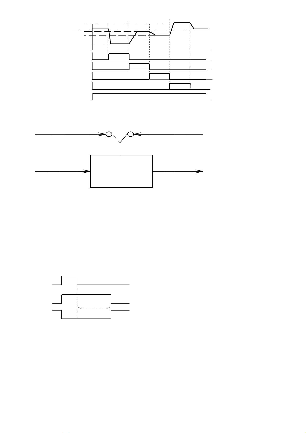
34
Normal Speed
DI2(28)
TMIA(DIx=7)
TMOA(DOx=14)
Pr.27
Pr.21
Pr.24
Pr.19
JOG
SPD1
SPD2
SPD3
time
time
time
time
time
RUN
time
8.6 DIx_Select = 6, OH (Over Heat) function (Also refer to Section 8.30)
When the input terminal is activated, the inverter will disable the output transistors, and show OH alarm message on the
display. Refer to mode-30, for complementary function.
8.7 DIx_Select = 7, TMIA
Clock In
or DI4(28)
or TMIB(DIx=11)
or TMIC(DIx=36)
Timer/Counter
Functional block diagram of Timer/Counter module
Internal Time Base
(0.1 Second)
or TMOB(DOx=20)
or TMOC(DOx=42)
Note: Only when select DI2(28) or DI4(28), the Timer/Counter Module will be configured as Counter Module.
Otherwise, it is configured as Timer Module.
When configured as a Timer, the Internal 0.1 Second time base signal is selected to be the clock input of the
Timer/Counter Module.
If configured as a Counter, the terminal of DI2 & DI4 that was assigned to mode-28 will become the clock input of the
Timer/Counter Module.
When digital input DIx is assigned to TMIA function, it serves as Input of the OFF-DELAY timer. User must assign a
digital output DOx , which select TMOA function to serve as the output of this timer. And the timer time will be
defined in Pr.71. (Refer to Sec.8.94)
When the timer input TMIA is ON, the timer output TMOA will be ON immediately.
If the TMIA become OFF, the timer will start counting time. After waiting the specified time period of Pr.71, then the
TMOA become OFF too.
TMIA
Note:
When use as Counter mode, the maximum clock input rate is
TMOA
Pr.71
1000Hz. There is only one internal Timer/Counter Block; you can
use only one Timer/Counter, either TYPE A or TYPE B or TYPE
C.
/TMOA
8.8 DIx_Select = 8, ON-BB
When any DIx selecting this function, activate the input DIx will BLOCK the BASE signal to all transistors
immediately in order to disable the inverter output. When the input is OFF again, the inverter will execute Speed Search
process.
Refer to Sec.11, the special function for Speed Search process.
Also Refer to Sec.8.18 for complement function.
8.9 DIx_Select = 9, FJR
When selected DIx is ON, it will force the inverter execute Forward-Jog-Run without RUN Command.
8.10 DIx_Select = 10, RJR
When selected DIx is ON, it will force the inverter execute Reverse-Jog-Run without RUN Command.
Page 36
35
8.11 DIx_Select = 11, TMIB
Refer to the functional block diagram of Timer/Counter module in Sec.8.7.
TMIB
Pr.71
TMOB
/TMOB
8.15 DIx_Select = 15, CLEAR the content of UP/DOWN COUNTER to Pr.16
8.16 DIx_Select = 16, LOAD the content of UP/DOWN COUNTER to Pr.15
8.17 DIx_Select = 17, HOLD the UP/DOWN COUNTER
Refer to Sec.7.6 Functional Block Diagram of Internal UP/DOWN counter.
Note: These digital function may be selected as the input terminals when Pr.40=6, 7 and 19, using the content of the
UP/DOWN counter as the NORMAL_SPEED_REQUEST.
If DIx(15) is ON, selects CLEAR function, the content of the internal UP/DOWN COUNTER will be set to Pr.16
(Lower Limit).
If DIx(16) is ON, selects LOAD function, the content of the internal UP/DOWN COUNTER will be set to Pr.15 (Upper
Limit).
If DIx(17) is ON, selects HOLD function, the UP/DOWN COUNTER will hold its value.
8.18 DIx_Select = 18, OFF-BB
When any DIx selecting this function, the input terminal must remain in activate state for normal operation. If the input
terminal is left open to OFF state, it will BLOCK the BASE signal to all transistors immediately in order to disable the
inverter output.
When the input is ON again, the inverter will execute Speed Search process. Refer to Sec.11, the special function for
Speed Search process.
Also Refer to Sec.8.8 for complement function.
8.19 DIx_Select = 19, UP
If DIx(19) is ON, the UP/COUNTER will increase its value, according to the acceleration rate specified in Pr.01.
8.20 DIx_Select = 20, DOWN
If DIx(20) is ON, the UP/COUNTER will decrease its value, according to the deceleration rate specified in Pr.02.
8.21 DIx_Select = 21, ALARM CLEAR
If user choose this function, then activate the DIx terminal will reset the inverter only when alarm had occurred.
Note: The RST terminal is used to RESET the whole inverter no matter alarm occurred or not.
8.22 DIx_Select = 22, SET Flip/Flop-1
8.23 DIx_Select = 23, CLEAR Flip/Flop-1
8.24 DIx_Select = 24, SET Flip/Flop-2
8.25 DIx_Select = 25, CLEAR Flip/Flop-2
8.26 DIx_Select = 26, SET both Flip/Flop-1 & Flip/Flop-2
8.27 DIx_Select = 27, CLEAR both Flip/Flop-1 & Flip/Flop-2
Two general purpose Flip/Flops were built in for many applications in order to minimize the necessary external
components. Each Flip/Flop block has two SET inputs, two CLEAR inputs and two complementary outputs for free
selection.
For example, Let
DI1_Select (Pr.41) = 22, select DI1 to be the SET input of FF1
DI2_Select (Pr.42) = 23, select DI2 to be the CLEAR input of FF1
DO1_Select (Pr.45)=32, select DO1 to be the output Q of FF1
then, the combination of inputs DI1, DI2 and output DO1 will serve as a Latch Relay.
Momentary ON signal apply to DI1 will cause DO1 enter ON state. On the contrary, ON signal apply to DI2 will cause
DO1 back to OFF state again.
If digital input function select is DIx_select=26, then ON input to DIx will SET both FF1 & FF2.
If digital input function select is DIx_select=27, then ON input to DIx will CLEAR both FF1 & FF2.
Note: Multiple assignment to the same input function is acceptable.
When digital input DIx is assigned to TMIB function, it serves as
Input of the ON-DELAY timer. User must assign a digital
output DOx, which select TMOB function to serve as the output
of this timer. And the timer time will be defined in Pr.71. (Refer
to Sec.8.94)
When the timer input TMIB is OFF, the timer output TMOB will
be OFF too.
Until the input TMIB is ON and continue ON for a specified
time period of Pr.71, then the TMOB will become ON.
8.12 DIx_Select = 12~14, reserve
Page 37
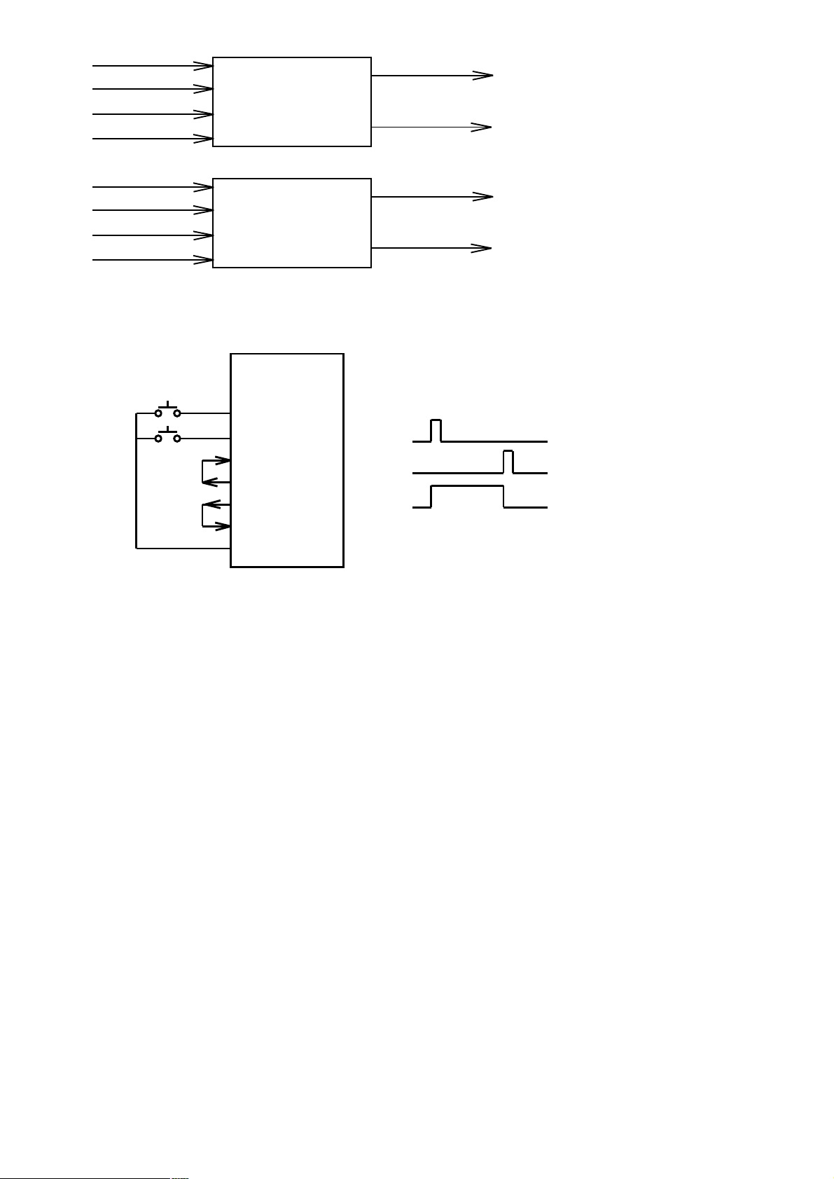
36
DIx=26
DIx=22
DIx=27
DIx=23
Set A
Set B
Clr A
Clr B
FF1
Q
_
Q
DOx=32
DOx=33
DIx=26
DIx=24
DIx=27
DIx=25
Functional Block diagram of Internal Flip/Flop Modules
Set A
Set B
Clr A
Clr B
FF2
Q
_
Q
DOx=34
DOx=35
Flip/Flop application example : Use DI1, DI2, DO1 as a LATCH RELAY.
Pr.41=22, Pr.42=23, Pr.43=23
Pr.45=4, Pr.46=32
START
STOP
RUN
START
STOP
ALARM
RUN
PDx-inverter
DI1
DI2
DI3
DO1
DO2
RUN
DCOM
8.28 DIx_Select = 28, CLOCK input of Timer/Counter
Refer to Sec.8.7, the Functional Block Diagram of the Internal Timer/Counter Module.
Note: Not every DIx input can select this function; only DI2(28) and DI4(28) are useful.
DI1(28): Used for AUTO-RUN mode, refer to Sec. 12 (for PDA/PDE/PDH series only)
DI2(28): Used for general purpose Timer/Counter, refer to Sec. 8.7, 8.11, 8.36.
DI3(28): No function
DI4(28): Used for AUTO-RUN mode, refer to Sec. 12 (for PDAN series only)
If this function is used, the Counter Module will advance one count when the input status of DIx changes from OFF to
ON.
The maximum input clock rate is limited to 1,000 Transitions/Second.
8.29 DIx_Select = 29, reserve
8.30 DIx_Select = 30, /OH function
When any digital input terminal select this function, it must remain in ON state for normal operation.
Else if the input is OFF, the inverter will disable the output transistors, and show OH alarm message on the display.
Refer to mode-6, for complementary function.
8.31 DIx_Select = 31, Normal/Auto Switch
Refer to Sec.12, the description of AUTO RUN Function.
Parameter Pr.72 determines the Auto Run Mode of the inverter.
This Digital Input function provides an easy way to change between Normal or Auto Run mode.
When the selected DIx input is OFF, then Pr.72 determines the inverter running mode.
If the input is ON, then it will force the inverter to run under Normal mode (equal to Pr.72=0).
Note: a. If Pr.72=0, selects Normal Run Mode.
b. The status change of the DIx will be effective only when the inverter is stop.
8.32 DIx_Select = 32~35, reserve
Page 38
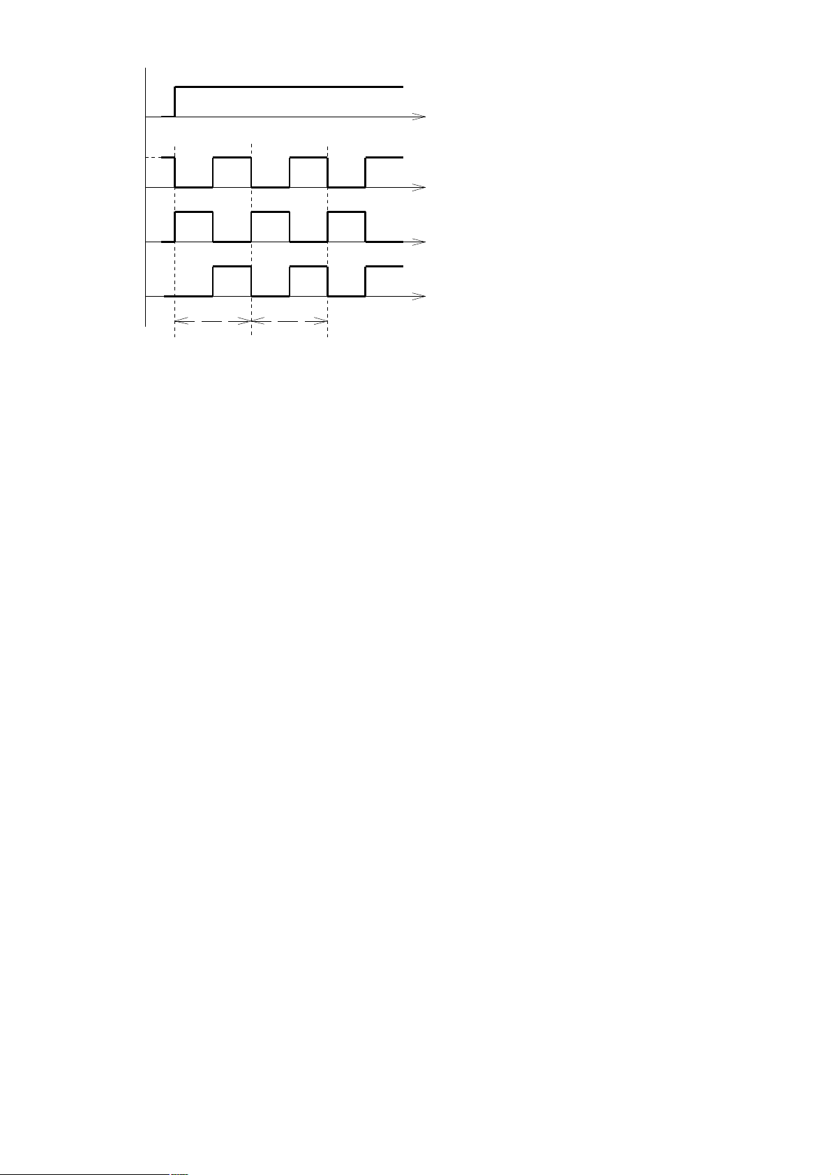
37
8.36 DIx_Select = 36, TMIC, start Astable Timer/Counter
TMIC
DIx(36)
If the input TMIC is OFF, the output TMOC is always
under ON state.
When the TMIC is ON, then the TMOC will start the
TMOC
DOx(42)
Astable ON/OFF cycle.
The period of time for one ON/OFF cycle is determined
by Pr.71. (Refer to Sec.8.94)
The duty cycle is 50%.
/TMOC
DOx(43)&
DOx(93)
TMOC
DOx(92)
If TMOC assigned by DOx(92), the TMOC output will
remain OFF, when TMIC is OFF.
Pr.71Pr.71
8.37 DIx_Select = 37~47, reserve
8.48 DIx_Select = 48, Speed Hold
When DIx(48) is ON, the inverter will stop ramp up or ramp down, and hold on present running speed.
If DIx(48) change to OFF, the inverter will resume ramp up or ramp down.
8.49 DIx_Select = 49, reserve
8.50 DIx_Select = 50, PID Enable
8.51 DIx_Select = 51, PID Hold
8.52 DIx_Select = 52, PID Clear
8.53 DIx_Select = 53, PID Preset
8.54 DIx_Select = 54, PID Bias Enable
8.55 DIx_Select = 55, PID Boost Enable
Refer to Appendix A
8.56 DIx_Select = 56~68, reserve
8.69 DC-BRAKE1
8.70 DC-BRAKE2
8.71 DC-BRAKE3
When set DIx(69 or 70 or 71) ON, the inverter will start injecting a continuous DC current into the motor winding.
Under this application, AI1, AI2 or AI3 are used to define the level of the injection current respectively.
The actual DC output voltage level is defined by Pr.06*Aix.
8.72 SENSOR-LESS Mode Change (for PDAN/PDA series only)
DIx(72) is used to toggle the operating mode between SENSOR-LESS and NON-SENSOR-LESS externally.
If Pr.67=1, and DIx(72)=ON, mode will change from Non-Sensor-Less to Sensor-Less.
If Pr.67=3, and DIx(72)=ON, mode will change from Sensor-Less to Non-Sensor-Less.
8.73 RUN function
8.74 REV function
Any digital input terminal assigned as DIx(73) will function as RUN terminal input.
Any digital input terminal assigned as DIx(74) will function as REV terminal input.
Refer to section 6 for detail RUN and REV terminal function.
8.75 Power Control Input Selection (for PDAN/PDA series only)
This function is only available under Pr.67=4, the Power Control mode.
When DIx(75) is ON, AI2 is selected in order to modify the POWER-LIMIT-CURVE.
Otherwise, if DIx(75) is OFF, or not any DIx(75) is assigned, AI3 is selected.
Refer to section 4.3.4.
8.76 FORWARD INHIBIT (for PDAN series only)
8.77 REVERSE INHIBIT (for PDAN series only)
If DIx(76)=ON, Forward Run is inhibited.
If DIx(77)=ON, Reverse Run is inhibited.
8.78 DIx_Select = 79, Increase the Panel Set frequency
8.78 DIx_Select = 79, Decrease the Panel Set frequency
While using Panel Set frequency as speed command (Pr.40=8),
if DIx(78)=ON, can increase the Panel Set frequency, and
if DIx(79)=ON, can decrease the Panel Set frequency.
8.80 DIx_Select = 80~83, 16 STEP-Speed select
DIx(80)~DIx(83) are used to assign 16-step frequency.
If DIx(2)~DIx(5) are all OFF, (no JOG, SPD1, SPD2, SPD3 function)
and if any of DIx(80)~DIx(83) is ON, then the set speed is:
Set Frequency = DIx(83)*Pr.27 + DIx(82)*Pr.24 + DIx(81)*Pr.21 + DIx(80)*Pr.19
Page 39
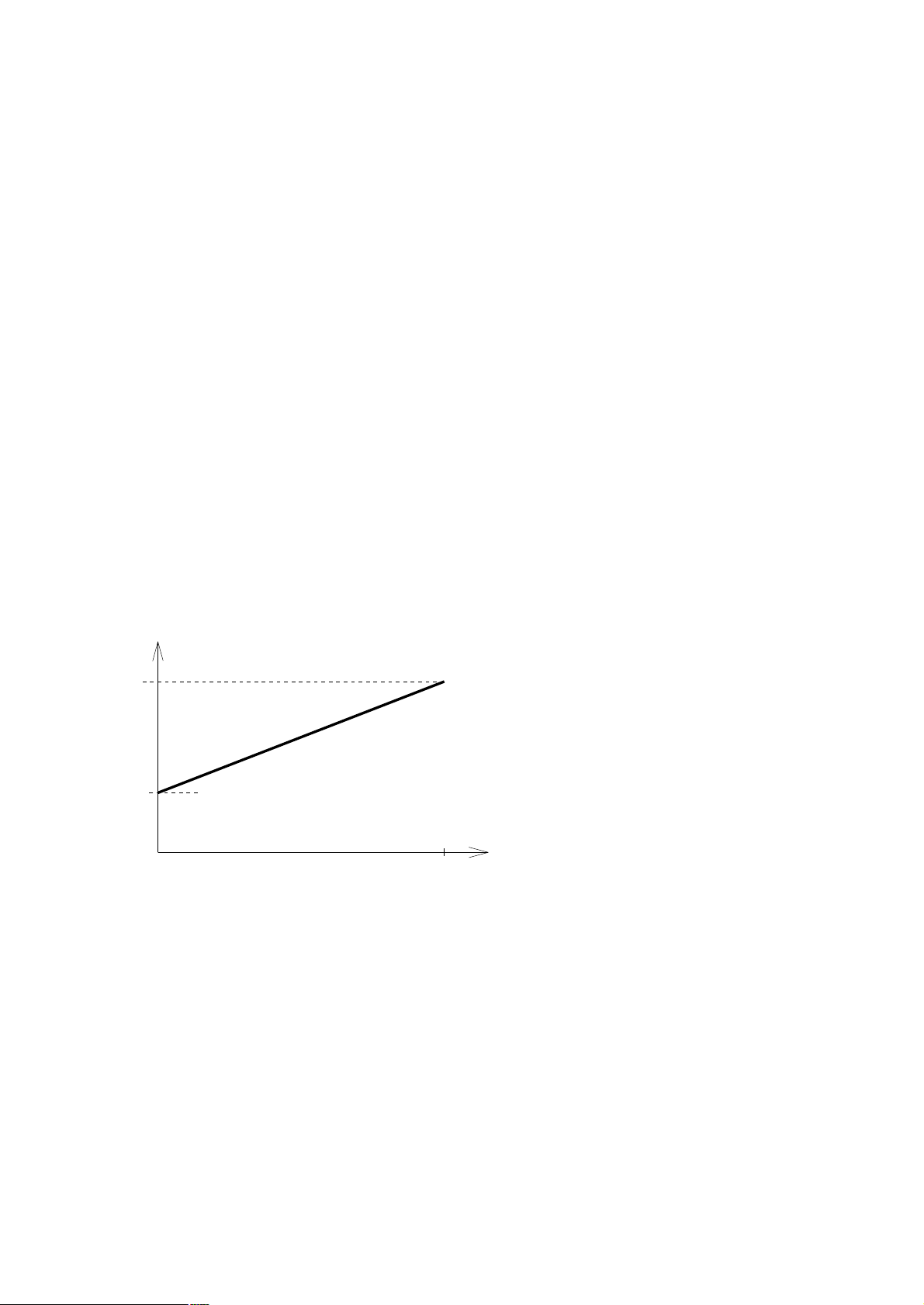
38
8.84 DIx_Select = 84~87, Select different ACC/DEC rate
If DIx(2)~DIx(5) are all OFF, then DIx(84)~DIx(87) can be used to select or change ACC/DEC rate.
DIx(84): select ACC=Pr.20, DEC=Pr.20
DIx(85): select ACC=Pr.22, DEC=Pr.23
DIx(86): select ACC=Pr.25, DEC=Pr.26
DIx(87): select ACC=Pr.28, DEC=Pr.29
8.88 DIx_Select = 88~90, Change COMMAND source
Refer to the definition of Pr.39 and Pr.40 in section 6 and section 7.
Pr.39 = a . b; contains selection a or b
Pr.40 = cc . dd; contains selection cc or dd
DIx(88) ON : Speed Command source = dd
DIx(88) OFF: Speed Command source = cc
DIx(89) ON: Control Command source = b
DIx(89) OFF: Control Command source = a
DIx(90) ON: Speed Command source = dd , and Control Command source = b
DIx(90) OFF: Speed Command source = cc , and Control Command source = a
Note: If any DIx(90) is selected, do not assign DIx(88) and DIx(89)
8.91 DIx_Select = 91, /TMIA
Complementary function of TMIA, refer to sec.8.7.
8.92 DIx_Select = 92, /TMIB
Complementary function of TMIB, refer to sec.8.11.
8.93 DIx_Select = 93, /TMIC
Complementary function of TMIC, refer to sec.8.36.
8.94 DIx_Select = 94~99, TIMER TIME MODIFICATION
DIx(94) = TMIAX
DIx(95) = TMIBX
DIx(96) = TMICX
DIx(97) = /TMIAX
DIx(98) = /TMIBX
DIx(99) = /TMICX
Similar to TIMA~TMIC, but the time can be varied by AI2 input.
T (Timer Time)
Pr.71
Pr.71*(Pr.91/1024)
AI2 input
+5V
Page 40
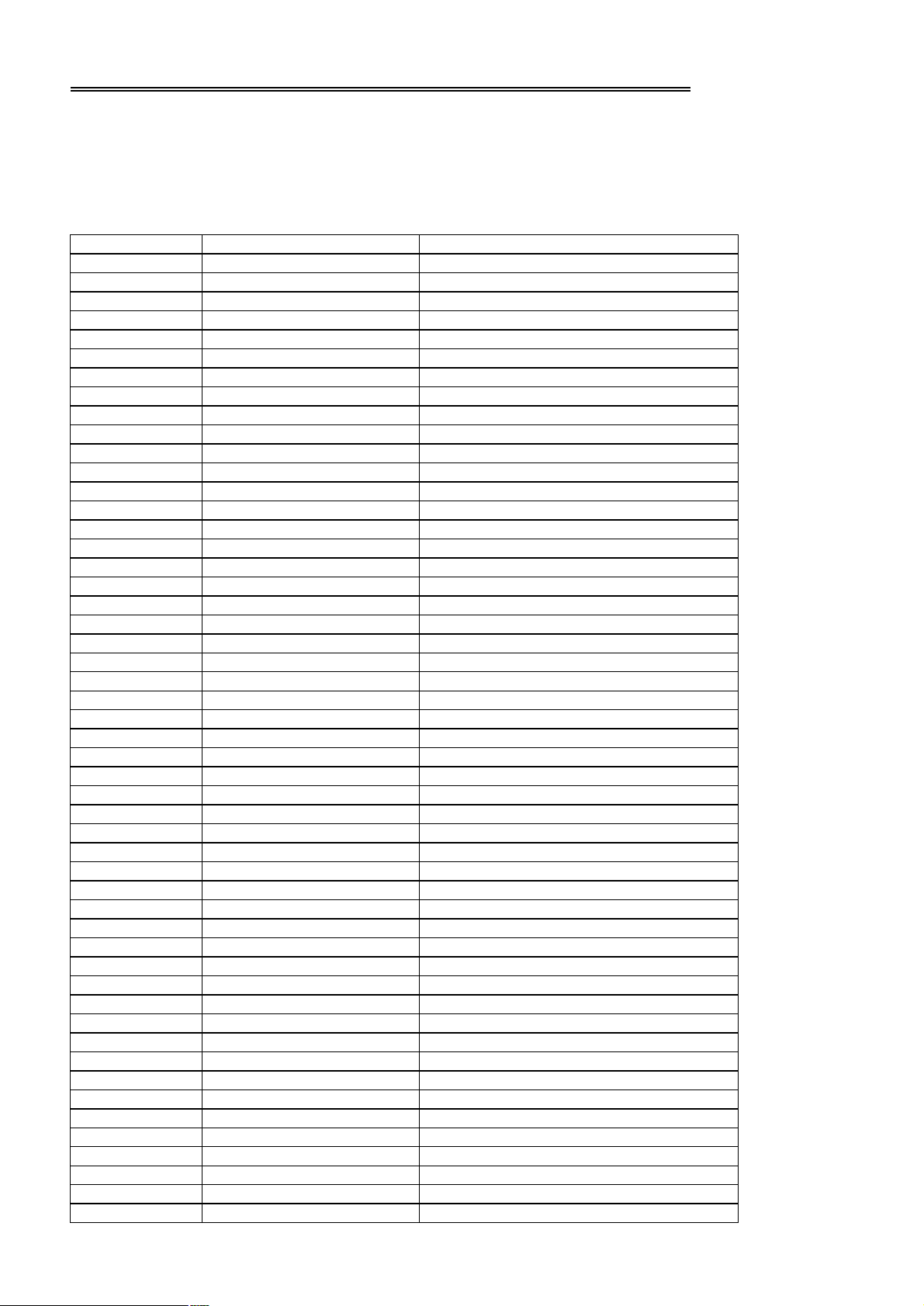
39
9. Selection of Digital output and Relay function
The DO1, DO2, RY1 and RY2 terminals are defined as multi-functional DIGITAL OUTPUTS.
The output circuit structure of DO1 & DO2 is Transistor OPEN COLLECTOR outputs.
The RY1and RY2 pair terminals are NORMAL OPEN(1a) contacts of the output RELAY.
The parameters for configuring the digital outputs are:
Pr.45 -- DO1_SELECT, used for DO1 output function select
Pr.46 -- DO2_SELECT, used for DO2 output function select
Pr.47 -- RELAY_SELECT, used for Relay output function select
Each of the three digital outputs may select any of the following output functions:
Pr.45,46,47 FUNCTION COMMENT
0 OFF ALWAYS OFF
1 NOT RUN NOT RUNNING
2 SPE SPEED EQUAL
3 SPNE SPEED NOT EQUAL
4 ALM ALARM
5 NALM NO ALARM
6 BRAKING UNDER BRAKING
7 RUNNING UNDER RUNNING
8 SPO SPEED OVER
9 SPNO SPEED NOT OVER
10 SPA SPEED ARRIVE
11 SPNA SPEED NOT ARRIVE
12 DIR OUTPUT DIRECTION
13 IRMS-LEVEL0 Irms>Pr.48
14 TMOA TIMER OUTPUT TYPE A
15 SPZ ZERO SPEED
16 SPNZ NOT ZERO SPEED
17 STALLING OUTPUT WHILE STALLING
18~19 Reserve
20 TMOB TIMER OUTPUT TYPE B
21 STEP1 AUTO RUNNING AT STEP 1
22 STEP2 AUTO RUNNING AT STEP 2
23 STEP3 AUTO RUNNING AT STEP 3
24 STEP4 AUTO RUNNING AT STEP 4
25 STEP5 AUTO RUNNING AT STEP 5
26 STEP6 AUTO RUNNING AT STEP 6
27 STEP7 AUTO RUNNING AT STEP 7
28 STEP8 AUTO RUNNING AT STEP 8
29 STEP9 AUTO RUNNING AT STEP 9
30 STEP10 AUTO RUNNING AT STEP 10
31 Reserve
32 Q1(FF1) Output of Flip/Flop-1
33 /Q1(FF1) Complement Output of FF1
34 Q2(FF2) Output of Flip/Flop-2
35 /Q2(FF2) Complement Output of FF2
36~37 Reserve
38 ALWAYS ON The Output terminal always ON
39 Reserve
40 /TMOA Complement of TMOA
41 /TMOB Complement of TMOB
42 TMOC TIMER OUTPUT TYPE C
43 /TMOC Complement of TMOC
44 X32CLK (only DO1) Output clock rate = 32 * Pr.57 (HZ)
45 X16CLK (only DO1) Output clock rate = 16 * Pr.57 (HZ)
46 X8CLK (only DO1) Output clock rate = 8 * Pr.57 (HZ)
47 X4CLK (only DO1) Output clock rate = 4 * Pr.57 (HZ)
48 X26CLK (only DO1) Output clock rate = 2 * Pr.57 (HZ)
49 X1CLK (only DO1) Output clock rate = 1 * Pr.57 (HZ)
50 IDC-LEVEL0 Idc>Pr.48 (PDA/PDH series only)
51 IDC-LEVEL1 Idc>AI1 (PDA/PDH series only)
52 IDC-LEVEL2 Idc>AI2 (PDA/PDH series only)
Page 41
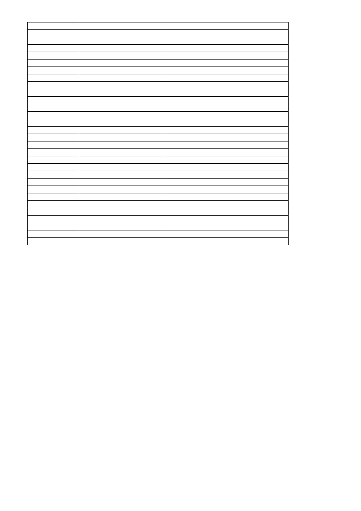
40
Pr.45,46,47 FUNCTION COMMENT
53 IDC-LEVEL3 Idc>AI3 (PDA/PDH series only)
54 IRMS-LEVEL1 Irms>AI1
55 IRMS-LEVEL2 Irms>AI2
56 IRMS-LEVEL3 Irms>AI3
57 POWER-LIMIT Under Power-Limit status (PDAN series only)
58~69 Reserve
70 RUN & AI1-Compare-HIGH RUNNING & AI1 > Pr.74
71 RUN & AI1-Compare-LOW RUNNING & AI1 < Pr.74
72 RUN & AI2-Compare-HIGH RUNNING & AI2 > Pr.75
73 RUN & AI2-Compare-LOW RUNNING & AI2 < Pr.75
74 RUN & AI3-Compare-HIGH RUNNING & AI3 > Pr.76
75 RUN & AI3-Compare-LOW RUNNING & AI3 < Pr.76
76~77 Reserve
78 OL-WARNING OL level >50%
79 /OL-WARNING OL level <50%
80 AI1-Compare-HIGH AI1 > Pr.74
81 AI1-Compare-LOW AI1 < Pr.74
82 AI2-Compare-HIGH AI2 > Pr.75
83 AI2-Compare-LOW AI2 < Pr.75
84 AI3-Compare-HIGH AI3 > Pr.76
85 AI3-Compare-LOW AI3 < Pr.76
86 ACCELERATING Under acceleration status
87 DECELERATING Under Deceleration status
88 DISCHARGING Under Discharging status
89 Reserve
90 FWD FORWARD RUNNING
91 REV REVERSE RUNNING
92 TMOC TMOC ENABLE AFTER TMIC ON
93 /TMOC Same as DOx(43)
Note: When power on, or the inverter will executing INITIALIZE function, all of the outputs will go OFF for a short
period of reset.
9.0 NULL function
The output status of DOx will always under OFF state when selecting this mode.
This function is complement function of Always ON function. Refer to Sec.9.38.
This function is useful when a master computer controls the inverter. The master computer can control these digital
outputs for other peripheral, independent to the inverter operation.
9.1 NOT RUNNING function (complement of Sec.9.7)
The output status of DOx will be ON when the inverter is under standby mode.
Inverter under standby mode means the output transistors are all OFF.
If the inverter starts running or under DC injection braking mode, the output status will become OFF.
Page 42
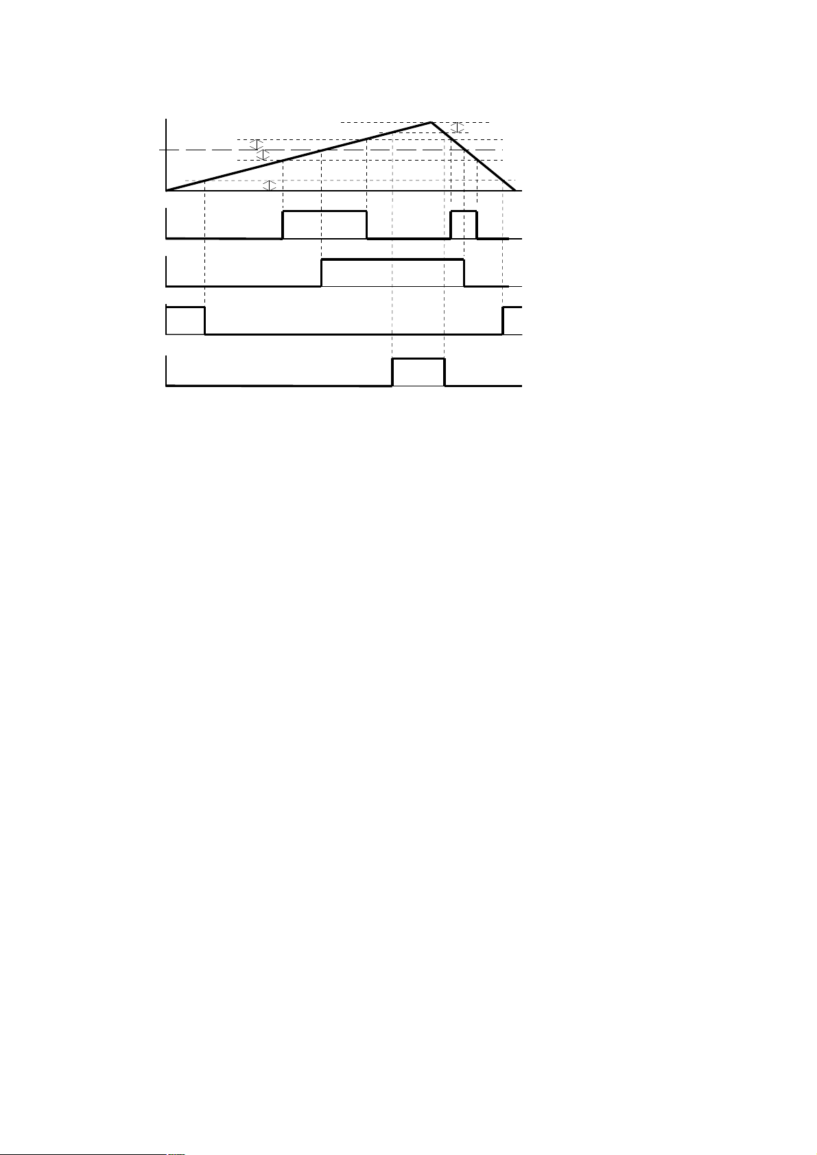
41
9.2 SPE Speed Equal function
9.3 SPNE Speed Not Equal function (complement of Sec.9.2)
HZ output
Set Frequency
Pr.49
Pr.50
Pr.50
Pr.50
Pr.50
time
SPE
time
SPO
SPZ
SPA
time
time
time
The output status of DOx(2) will ON, if the output frequency is EQUAL to the preset frequency defined in Pr.49.
Definition of EQUAL means: Difference is within the allowable tolerance defined in Pr.50.
* Relative functions are SPO, SPZ, and SPA.
9.4 ALARM output function (complement of Sec.9.5)
The output status of DOx(4) is normally OFF when the inverter detects no error.
If error occurs, the output DOx(4) will ON immediately.
9.5 NOT ALARM output function (complement of Sec.9.4)
DOx(5) = /DOx(4)
9.6 BRAKING function (Refer to Section 5.4, Pr.05~Pr.08)
The output DOx(6) will ON, when the inverter is under DC injection braking mode.
9.7 RUNNING function (Refer to Section 5.4, Pr.05~Pr.08)
The output DOx(7) is OFF when the inverter is under standby mode (not running).
If the inverter starts running or under DC injection braking mode, the output DOx(7) will ON.
9.8 SPO Speed Over function (Refer to Section 9.2)
The output status of DOx(8) will ON, if the absolute value of output frequency is OVER the preset frequency defined
in Pr.49. (i.e. Pr.57>Pr.49)
9.9 SPNO Speed Not Over function (complement of Sec.9.8)
DOx(9) = /DOx(8)
9.10 SPA Speed Arrive function (Refer to Section 9.2)
The output status of DOx will ON, if the output frequency is EQUAL to the Set frequency.
Definition of EQUAL means: Difference between output Hz and desired frequency is within the allowable
tolerance defined in Pr.50.
Note: the SPA signal is always OFF if inverter is not running or is under DC injection braking.
9.11 SPNA Speed Not Arrive function (complement of Sec.9.10)
DOx(11) = /DOx(10)
9.12 DIRECTION output function
The output status of DOx(12) will ON, if the output frequency >=0.
The output status of DOx will be OFF, if the output frequency <0 .
Refer to Sec.9.90 & 9.91
9.13 IRMS-LEVEL0
DOx(13) output will ON, if Irms>Pr.48.
Irms is root mean square current value of inverter output.
9.14 TMOA Timer Output A-type function (Refer to Section 8.7)
Refer to the Functional block diagram of Timer/Counter module in Sec.8.7 and the related descriptions.
9.15 SPZ Speed Zero function (Refer to Section 9.2)
The output status of DOx will ON, if the output frequency is EQUAL to Zero. (Pr.57<Pr.50)
9.16 SPNZ Speed Not Zero function (complement of Sec.9.15)
DOx(16) = /DOx(15)
9.17 STALLING function
While inverter running, if the output current exceeds hardware limit (150%), the output frequency will decrease
automatically to reduce the output current. Inverter running under such condition is called Stalling, and output status
DOx(17) will become ON to indicate this situation.
9.18~19 reserve
Page 43

42
9.20 TMOB Timer Output B-type function (Refer to Section 8.11)
Refer to the Functional block diagram of Timer/Counter module in Sec.8.7 and the related descriptions in Sec.8.11.
9.21 STEP1 output indicating Auto running at step1 (Refer to Section 12.2)
9.22 STEP2 output indicating Auto running at step2 (Refer to Section 12.2)
9.23 STEP3 output indicating Auto running at step3 (Refer to Section 12.2)
9.24 STEP4 output indicating Auto running at step4 (Refer to Section 12.2)
9.25 STEP5 output indicating Auto running at step5 (Refer to Section 12.2)
9.26 STEP6 output indicating Auto running at step6 (Refer to Section 12.2)
9.27 STEP7 output indicating Auto running at step7 (Refer to Section 12.2)
9.28 STEP8 output indicating Auto running at step8 (Refer to Section 12.2)
9.29 STEP9 output indicating Auto running at step9 (Refer to Section 12.2)
9.30 STEP10 output indicating Auto running at step10 (Refer to Section 12.2)
9.31 Reserve
9.32 Q1 output of Flip/Flop-1 (Refer to Section 8.22)
DOx(32) is Q output of Flip/Flop-1.
9.33 /Q1 output of Flip/Flop-1 (Refer to Section 8.22)
DOx(33) is /Q output of Flip/Flop-1.
9.34 Q2 output of Flip/Flop-2 (Refer to Section 8.22)
DOx(34) is Q output of Flip/Flop-2.
9.35 /Q2 output of Flip/Flop-2 (Refer to Section 8.22)
DOx(32) is /Q output of Flip/Flop-2.
9.36~37 Reserve
9.38 Always ON
The output status of DOx(38) is always under ON state when selecting this mode.
This function is complement function of NULL function. Refer to Sec.9.0.
This function is useful when the inverter is controlled by a master computer, or under TEST mode.
The master computer can control these digital outputs for other peripheral, independent to the inverter operation.
9.39 reserve
9.40 /TMOA Complement function of TMOA
DOx(40) = /DOx(14)
9.41 /TMOB Complement function of TMOB
DOx(41) = /DOx(20)
9.42 TMOC Timer Output C-type function (Refer to Section 8.36)
9.43 /TMOC Complement function of TMOC
DOx(43) = /DOx(42)
9.44 X32CLK output clock rate = 32 * Pr.57 (HZ)
9.45 X16CLK output clock rate = 16 * Pr.57 (HZ)
9.46 X8CLK output clock rate = 8 * Pr.57 (HZ)
9.47 X4CLK output clock rate = 4 * Pr.57 (HZ)
9.48 X2CLK output clock rate = 2 * Pr.57 (HZ)
9.49 X1CLK output clock rate = 1 * Pr.57 (HZ)
DOx(44)~DOx(49) are used for generating an output clock.
The maximum output clock rate should limit within 3KHz.
This clock output is only available for DO1.
After select one of these functions, user must execute RESET in order to change DO1 into XnCLK function. On the
contrary, if change from XnCLK into other DOx function, also execute RESET after selection is changed.
9.50 IDC-LEVEL0
DOx(50) output will ON, if Idc>Pr.48.
Idc is current value in DC bus.
Note: this function is for PDA/PDH series only.
9.51 IDC-LEVEL1
DOx(51) is similar to DOx(50), but AI1 is used as the comparison level.
Actual comparison method is : Idc(%) > 150% * AI1
Note: this function is for PDA/PDH series only.
9.52 IDC-LEVEL2
DOx(52) is similar to DOx(50), but AI2 is used as the comparison level.
Actual comparison method is: Idc(%) > 150% * AI2
Note: this function is for PDA/PDH series only.
9.53 IDC-LEVEL3
DOx(53) is similar to DOx(50), but AI3 is used as the comparison level.
Actual comparison method is: Idc(%) > 150% * AI3
Note: this function is for PDA/PDH series only.
Page 44

43
9.54 IRMS-LEVEL1
DOx(54) is similar to DOx(13), but AI1 is used as the comparison level.
Actual comparison method is : Irms(%) > 150% * AI1
9.55 IRMS-LEVEL2
DOx(55) is similar to DOx(13), but AI2 is used as the comparison level.
Actual comparison method is: Irms(%) > 150% * AI2
9.56 IRMS-LEVEL3
DOx(56) is similar to DOx(13), but AI3 is used as the comparison level.
Actual comparison method is: Irms(%) > 150% * AI3
9.57 POWER-LIMIT
DOx(57) will ON, if under Power-Limit condition. (Refer to section 4.3.4)
9.58 ~ 9.69 reserve
9.70 RUN & AI1-COMPARE-HIGH
9.71 RUN & AI1-COMPARE-LOW
9.72 RUN & AI2-COMPARE-HIGH
9.73 RUN & AI2-COMPARE-LOW
9.74 RUN & AI3-COMPARE-HIGH
9.75 RUN & AI3-COMPARE-LOW
DOx(70)~DOx(75) are used to detect the input level of AIx and inverter running respectively.
Pr.74 is used as the comparison level for AI1.
Pr.75 is used as the comparison level for AI2.
Pr.76 is used as the comparison level for AI3.
Under this application, the value of Pr.74, Pr.75 and Pr.76 should set in the range 0.0~1023.0.
AI1 input level can be monitored by checking Pr.56 when Pr.55=3.
AI2 input level can be monitored by checking Pr.56 when Pr.55=4.
AI3 input level can be monitored by checking Pr.56 when Pr.55=5.
Example: DOx(80) will ON, if inverter running and AI1 input level > Pr.74.
DOx(81) will ON, if inverter running and AI1 input level < Pr.74.
9.78 OL-WARNING
9.79 /OL-WARNING
The OL level can be monitored at Pr.61 when Pr.54=11.
DOx(78) will ON, if OL level >50%.
DOx(79) is complement function of DOx(78).
Refer to Pr.54, for monitoring the OL accumulation level.
9.80 AI1-COMPARE-HIGH
9.81 AI1-COMPARE-LOW
9.82 AI2-COMPARE-HIGH
9.83 AI2-COMPARE-LOW
9.84 AI3-COMPARE-HIGH
9.85 AI3-COMPARE-LOW
DOx(80)~DOx(85) are used to detect the input level of AIx respectively.
Pr.74 is used as the comparison level for AI1.
Pr.75 is used as the comparison level for AI2.
Pr.76 is used as the comparison level for AI3.
Under this application, the value of Pr.74, Pr.75 and Pr.76 should set in the range 0.0~1023.0.
AI1 input level can be monitored by checking Pr.56 when Pr.55=3.
AI2 input level can be monitored by checking Pr.56 when Pr.55=4.
AI3 input level can be monitored by checking Pr.56 when Pr.55=5.
Example: DOx(80) will ON, if AI1 input level > Pr.74.
DOx(81) will ON, if AI1 input level < Pr.74.
9.86 ACCELERATING
DOx(86) will ON, if inverter is increasing its output frequency.
9.87 DECELERATING
DOx(87) will ON, if inverter is decreasing its output frequency.
9.88 DISCHARGING
DOx(88) will ON, if the voltage of internal capacitor goes too high.
9.89 reserve
9.90 RUNNING FORWARD
DOx(90) = ON, when the inverter is Running in FORWARD direction.
9.91 RUNNING REVERSE
DOx(91) = ON, when the inverter is Running in REVERSE direction.
9.92 TMOC with Disable
When DIx(36)=TMIC is ON, this output function is the same as DOx(42).
If DIx(36) is OFF, then DOx(92) will always OFF.
9.93 /TMOC
Same as DOx(43)
Page 45
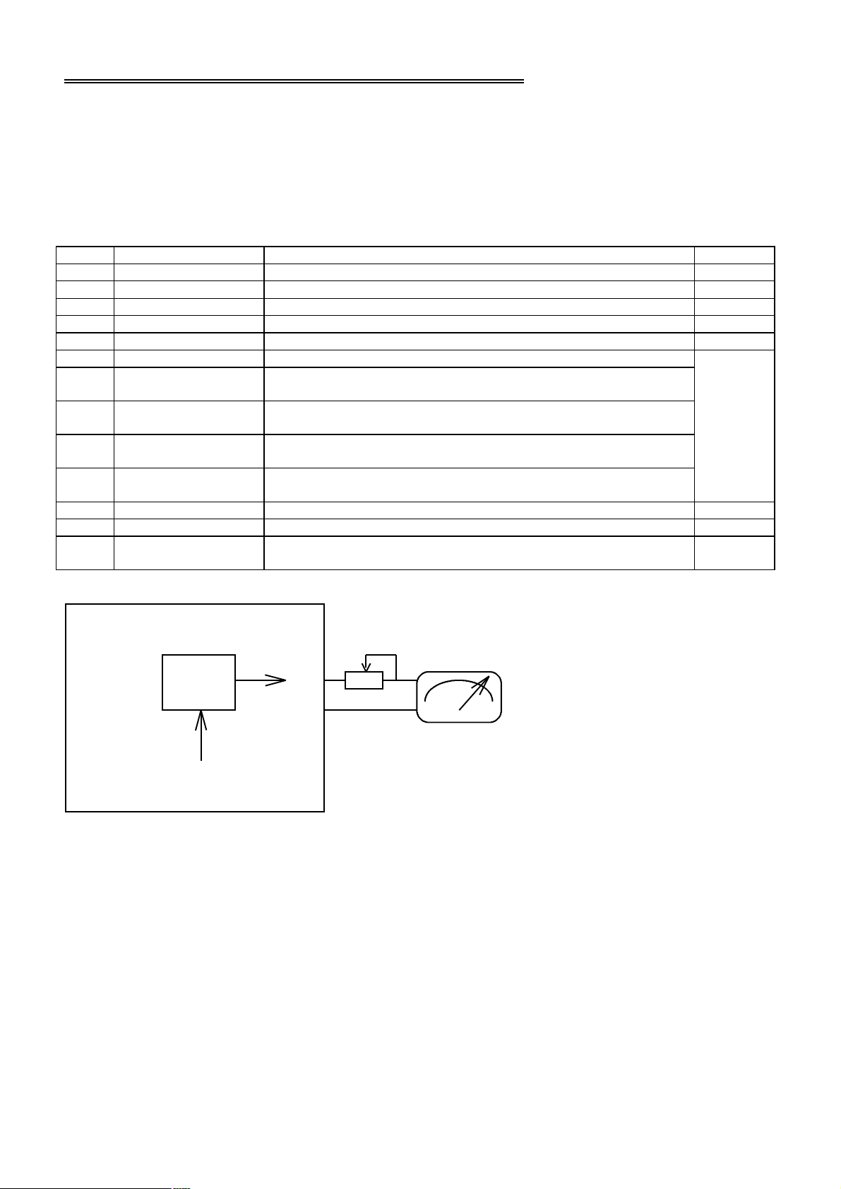
44
10. Selection of Analog output function
This section describes the definition of analog output voltage between "AM" & "ACOM".
Refer to Section-1.2.2 for the internal circuit structure.
Relative parameter
Pr.37 -- AM_SELECT
Pr.38 -- AM_GAIN
Auxiliary Analog Output Terminal "AM" is provided for analog meter display, or other applications
Requiring the analog output signal.
"AM_SELECT" is used to select desired signal, which will output to AM terminal.
"AM_GAIN" is used to fine tuning the output voltage level.
User may select any of the four signals in the Table for output to the "AM" terminal.
Pr.37 AM Terminal Function Output Ratio Remarks
0 HZ Signal +5V*((Pr.57) / (Pr.15))
1 Reserve
2 Vdc Signal +5V*((Pr.59) / 1000)
3 Vout Signal +5V*((Pr.60) / (2 * Pr.84))
4~6 Reserve
7 PID Output +5V*(PID Output)
8 PID Output +
Bias Input from AI1
9 PID Output +
Bias Input from AI2
10 PIDoutput +
Bias Input from AI3
11 PID Output +
Bias Set by Pr.28
12 Constant voltage +5V*((Pr.38)/255)
13~16 Reserve
17 Heat Sink Temperature +5V*((Pr.62)/100) For PDAN
Recommend interface circuit to external analog meter:
If DIx(54)=ON, +5V*(PID Boost * (PID Output + Bias Input from AI1))
If DIx(54)=OFF, +5V*(PID Boost * PID Output)
If DIx(54)=ON, +5V*(PID Boost * (PID Output + Bias Input from AI2))
If DIx(54)=OFF, +5V*(PID Boost * PID Output)
If DIx(54)=ON, +5V*(PID Boost * (PIDoutput + Bias Input from AI3))
If DIx(54)=OFF, +5V*(PID Boost * PID Output)
If DIx(54)=ON, +5V*(PID Boost * (PID Output + Bias Set by Pr.28))
If DIx(54)=OFF, +5V*(PID Boost * PID Output)
Refer to
Appendix
A
series only
PD inverter
Gain
(Pr.38)
AM
5k
ACOM
Desired output
signal select by Pr.37
First use Pr.37 to select desired output signal.
And let Pr.38=250.
Then adjust variable resistor for trimming to correct position.
If necessary, modify Pr.38 for fine-tuning.
Refer to Sec.1.2 for hardware structure.
Analog Meter
1V/1mA
Page 46
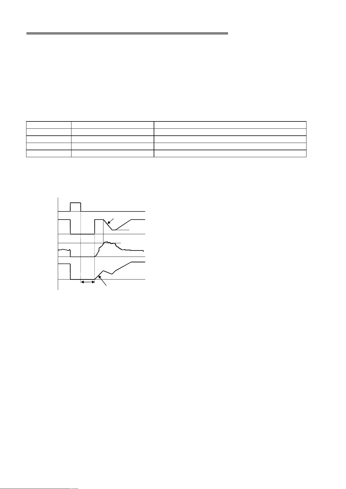
45
11. Speed search and Base Block function
*
time
Irms
Pr.79 to Pr.82 are used to define the inverter's speed searching characteristics for restart process.
The Speed Search function may be initiated by two methods:
By Digital Input to initiate the speed search process
Let DIx(8), selects "Base Block" function to any Digital input. If DIx(8) is ON, then the inverter will disable IGBT output
causing the motor FREE RUN to stop.
When DIx OFF again, the inverter will still remain in the BLOCK state for a period of time defined in the parameter BASE
BLOCK TIME (Pr.36). After the period of BASE BLOCK TIME, Then the restart process begins.
Power comes back normal after UP/OP alarm to initiate the speed search process
LET Pr.34 = 1, enables UP/OP restart function. If "UP" or "OP" alarm appear while inverter running, Then the inverter will
disable IGBT output causing the motor FREE RUN.
When Power come back to normal again, the inverter will still remain in the BLOCK state for a period of time defined in
the parameter BASE BLOCK TIME (Pr.36). After the period of BASE BLOCK TIME, Then the restart process begins.
PARAMETER FUNCTION DESCRIPTION
Pr.79 RESTART TYPE SELECT RESTART TYPE
Pr.80 RESTART STALL LEVEL STALL LEVEL WHILE RESTARTING
Pr.81 RESTART DEC TIME DEC TIME WHILE SPEED SEARCH
Pr.82 VOLTAGE RECOVER TIME VOLTAGE INCREASING RATE WHILE RESTARTING
Pr.79=0: No restart speed search process. Inverter will start from Pr.04.
Pr.79=1: Speed search begins from previous running frequency.
Pr.79=2: Speed search begins from UPPER LIMIT frequency (Pr.15).
Pr.79=3: Speed search begins from SET SPEED.
BB
Hz
Pr.81
Speed Match
time
time
Pr.80 (PDE=150%)
time
Vout
Pr.36
*Note: Pr.79 selects the search start frequency.
After BASE BLOCK TIME, the following steps describe the speed search process:
l Send out a frequency Hz which is selected by Pr.79, and Let Vout =0.
l Maintain the initial frequency, and increase the output voltage Vout according to the rate defined by Pr.82. During
this period, monitor the current until it reaches the level defined in Pr.80.
l Use Pr.81 as deceleration rate to decrease the output frequency Hz and output voltage Vout. Wait until Irms is less
than Pr.80 that means now the inverter output frequency matches the motor speed.
l Now the inverter output frequency can start ramp to desired target frequency.
Pr.82
Page 47
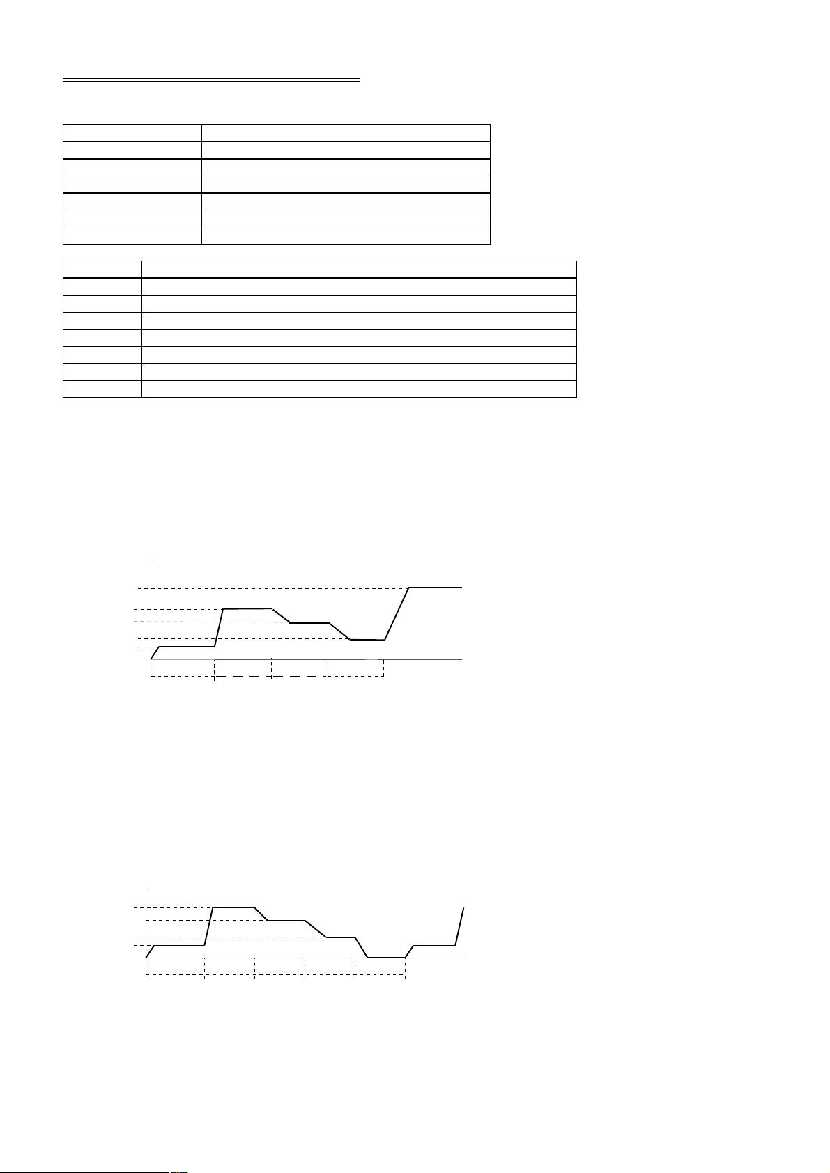
46
12. AUTO RUN Function
12.1 Auto Mode Selection & Running
TABLE OF PARAMETERS USED FOR AUTO MODE.
PARAMETER FUNCTION
Pr.72 AUTO MODE SELECT
Pr.73 AUTO STEP 1(or 6) JOG_SPD_PERIOD
Pr.74 AUTO STEP 2(or 7) SPD1_SPD_PERIOD
Pr.75 AUTO STEP 3(or 8) SPD2_SPD_PERIOD
Pr.76 AUTO STEP 4(or 9) SPD3_SPD_PERIOD
Pr.77 AUTO STEP 5(or 10) MANI_SPD_PERIOD
TABLE OF AUTO MODE FUNCTIONS
Pr.72 AUTO FUNCTION DESCRIPTION
0 NO AUTO FUNCTION
1 STEP RUN & MAINTAIN SPEED
2 STEP RUN, STOP & REPEAT
3 STEP RUN, STOP & CHANGE DIRECTION REPEAT
4 STEP RUN, & REPEAT
5 STEP RUN, & CHANGE DIRECTION REPEAT
6 SIMILAR TO MODE 4, BUT REPEAT FROM STEP2
Pr.72 = 1 STEP RUN & MAINTAIN
STEP1 inverter running as if JOG command is applied.
Pr.73 (JOG_PERIOD) determines time.
STEP2 inverter running as if SPD1 command is applied.
Pr.74 (SPD1_PERIOD) determines time.
STEP3 inverter running as if SPD2 command is applied.
Pr.75 (SPD2_PERIOD) determines time.
STEP4 inverter running as if SPD3 command is applied.
Pr.76 (SPD3_PERIOD) determines time.
STEP5 inverter running at specified MAIN speed as if it is in normal mode.
Pr.00
Pr.21
Pr.24
Pr.27
Pr.19
Pr.73
Example speed pattern of AUTO STEP RUN Type 1
Pr.72 = 2 STEP RUN, STOP & REPEAT
STEP1 inverter running as if JOG command is applied.
Pr.73 (JOG_PERIOD) determines time.
STEP2 inverter running as if SPD1 command is applied.
Pr.74 (SPD1_PERIOD) determines time.
STEP3 inverter running as if SPD2 command is applied.
Pr.75 (SPD2_PERIOD) determines time.
STEP4 inverter running as if SPD3 command is applied.
Pr.76 (SPD3_PERIOD) determines time.
STEP5 inverter running as if STOP command is applied.
Pr.77 (HALT_PERIOD) determines time.
AFTER STEP5, REPEAT FROM STEP1.
Pr.74
Pr.75
Pr.76
Pr.21
Pr.24
Pr.27
Pr.19
Pr.73Pr.74Pr.75Pr.76Pr.77
Example speed pattern of AUTO STEP RUN Type 2
REPEAT
time
Page 48
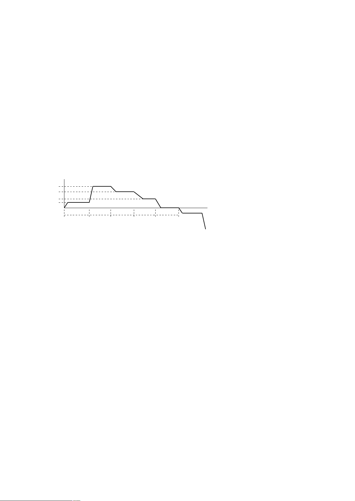
47
Pr.72 = 3 STEP RUN, STOP & CHANGE DIRECTION REPEAT
STEP1 inverter running as if JOG command is applied.
Pr.73 (JOG_PERIOD) determines time.
STEP2 inverter running as if SPD1 command is applied.
Pr.74 (SPD1_PERIOD) determines time.
STEP3 inverter running as if SPD2 command is applied.
Pr.75 (SPD2_PERIOD) determines time.
STEP4 inverter running as if SPD3 command is applied.
Pr.76 (SPD3_PERIOD) determines time.
STEP5 inverter running as if STOP command is applied.
Pr.77 (HALT_PERIOD) determines time.
AFTER STEP5, CHANGE DIRECTION
STEP6 inverter running as if JOG command is applied.
Pr.73 (JOG_PERIOD) determines time.
STEP7 inverter running as if SPD1 command is applied.
Pr.74 (SPD1_PERIOD) determines time.
STEP8 inverter running as if SPD2 command is applied.
Pr.75 (SPD2_PERIOD) determines time.
STEP9 inverter running as if SPD3 command is applied.
Pr.76 (SPD3_PERIOD) determines time.
STEP10 inverter running as if STOP command is applied.
Pr.77 (HALT_PERIOD) determines time.
AFTER STEP10, REPEAT FROM STEP1.
Pr.21
Pr.24
Pr.27
Pr.19
REVERSE
& REPEAT
Pr.73Pr.74Pr.75Pr.76Pr.77
Example speed pattern of AUTO STEP RUN Type 3
Pr.72 = 4 STEP RUN & REPEAT
This mode is similar to mode2.
From STEP1 to STEP4, its operation is exactly the same as mode2.
Under STEP5 period, the inverter will run at MAIN speed instead of STOP command.
AFTER STEP5, REPEAT FROM STEP1.
Pr.72 = 5 STEP RUN & CHANGE DIRECTION REPEAT
This mode is similar to mode3.
From STEP1 to STEP4, its operation is exactly the same as mode3.
Under STEP5 period, the inverter will run at MAIN speed instead of STOP command.
From STEP6 to STEP9, its operation is exactly the same as mode3.
Under STEP10 period, the inverter will run at MAIN speed instead of STOP command.
AFTER STEP10, REPEAT FROM STEP1.
Page 49
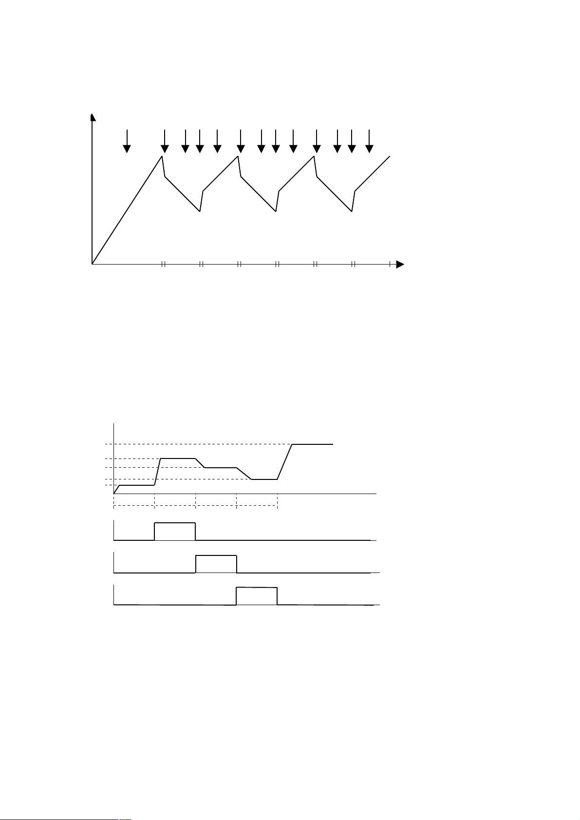
48
T1T2T3T4T5T2T3T4T5T2T3T4T5
Pr.72 = 6 STEP RUN & REPEAT from STEP-2
This mode is similar to mode4.
From STEP1 to STEP5, its operation is exactly the same as mode4.
After STEP5, the procedure jumps to STEP2 and repeat.
START: SETP1-->STEP2 ~ -->STEP5-->STEP2 ~ -->STEP5-->STEP2 ~ -->STEP5 ........
1 2 3 4 5 2 3 4 5 2 3 4 5
12.2 Auto Run Status Output
During AUTO RUNNING, there are special DOx functions reserved for AUTO STEP EQUAL application. (Refer to
Section 9.21~9.30)
EXAMPLE:
If user wishes to activate the DOx outputs when inverter is auto running,
if LET DO1(22), select STEP2
DO2(23), select STEP3
DO3(24), select STEP4
THEN DO1 terminal will become ON, while the inverter is running at STEP2
DO2 terminal will become ON, while the inverter is running at STEP3
RELAY terminals will become ON, while the inverter is running at STEP4
Pr.00
Pr.21
Pr.24
Pr.27
Pr.19
Pr.73Pr.74Pr.75Pr.76
DO1(22)
DO2(23)
RELAY(24)
EXAMPLE: Timing Relationship waveform of "STEP EQUAL OUTPUT " Function.
time
time
time
time
Page 50

49
13. MONITOR function
0000
. . . .
While Panel is in MON mode, user can select which two statuses are to be monitored.
Pr.98 is used to assign the parameter to be monitored, when "I" LED is on.
Pr.99 is used to assign the parameter to be monitored, when "HZ" LED is on.
For example, the default value in Pr.99 is 57. That means, 7-segment will display the value of Pr.57 while "HZ" LED is on.
Note: For PDE series, Irms (Pr.61)=0. User can choose another important parameter for monitoring.
13.1 Operating Status Check
Parameters from Pr.57 ~ Pr.61 are inverter running status for user monitoring purpose.
Pr.57 HZ HZ status shows the running frequency.
Pr.58 RPM RPM status is calculated by HZ status.
RPM = (120 * HZ / POLE) * GEAR_RATIO%
Refer to Section 5.4, description of Pr.52 & Pr.53.
Pr.59 Vdc Vdc is the DC voltage measured from internal Smoothing Capacitor.
Vdc = Pr.87(%) * Pr.56 (when Pr.55=0)
Pr.60 Vout Vout is the Root-Mean-Square value of inverter output voltage.
Pr.61 IRMS (or other status)
Through Pr.54, other status can be selected for display.
Pr.54=0: Irms (ampere)
Pr.54=1: Irms (% of inverter rating)
Pr.54=2: Irms (% of motor rating)
Pr.54=3: Power Angle q (Angle of Current Phase Lag)
Pr.54=4: Output VA= IrmsVrms **3
Pr.54=5: Power Factor PF= )cos(q
Pr.54=6: Watt (ac side) = )cos(***3
Pr.54=7: Idc (ampere) (For PDA/PDH series only)
Pr.54=8: Idc (% of inverter rating) (For PDA/PDH series only)
Pr.54=9: Watt (dc side) = Vcap*Idc (For PDA/PDH series only)
Pr.54=10: Watt (limit)
Pr.54=11: OL accumulation level
Pr.54=32: Shows timer value when it is used. (For PDAN series only)
Pr.62 TEMPERATURE of HEAT SINK in Centigrade.
IrmsVrms
q
13.2 Terminal Status Check
User can easily check the input or output terminal status from following parameters:
TERMINAL STATUS is easily verified by select the corresponding parameter number.
Pr.63 Digital Input Terminal Status
Monitors the DI1~DI4 input terminal status.
Digit 3: DI1 Input Terminal Status
Digit 2: DI2 Input Terminal Status
Digit 1: DI3 Input Terminal Status
Digit 0: DI4 Input Terminal Status
DI1
DI2 DI3 DI4
Input Terminal Status
Page 51
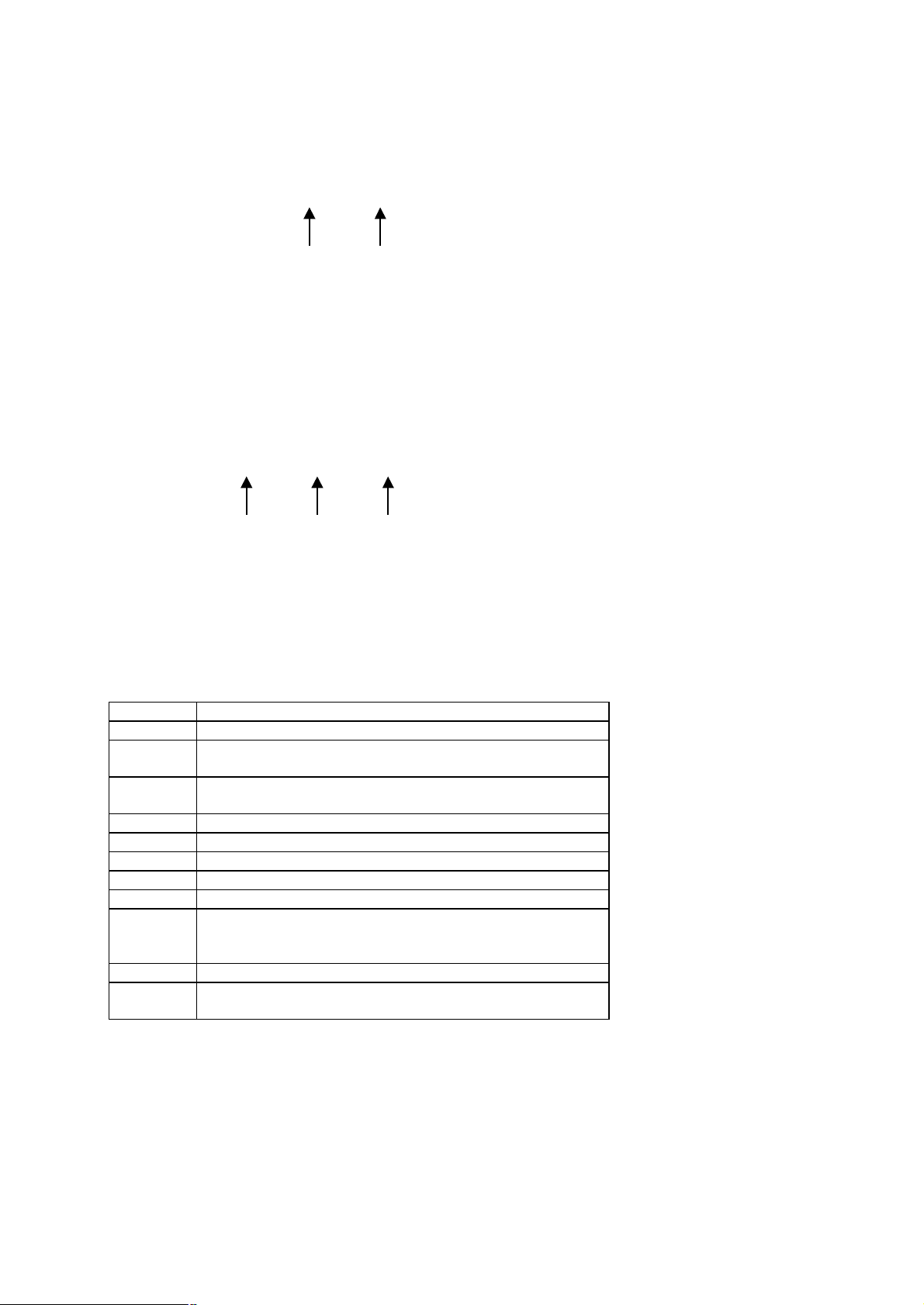
50
Pr.64 Control Input Terminal status
0000
. . . .
0 000
. . . .
Monitors the RUN & REV input terminal status.
Digit 1: RUN Input Terminal Status
Digit 0: REV Input Terminal Status
RUN
Control Input Terminal status
Pr.65 Digital Output Terminal Status
Monitors the DO1, DO2 & RY (1,2) output terminal status.
Digit 2: DO1 Output Terminal Status
Digit 1: DO2 Output Terminal Status
Digit 0: RELAY Output Status
DO1 DO2 RELAY
Digital Output Terminal Status
REV
13.3 A/D Converter Check
Pr.55 A/D CHANNEL SELECT
Pr.56 A/D CONVERSION DATA
Use Pr.55 to select the desired channel for monitoring, then the 10-bits A/D converter of CPU will execute Analog to
Digital conversion and put the conversion result in Pr.56.
The range of the converted data is from 0 to 1023 corresponding to full range input.
Pr.55 Pr.56 (A/D DATA)
0 VDC channel A/D value
1 Iv channel A/D value
Note: For PDAN series only.
2 Iw channel A/D value
Note: For PDAN series only.
3 AI1 channel A/D value
4 AI2 channel A/D value
5 AI3 channel A/D value
6 Thermistor A/D value
7 Reserve
8 Shows QUEUE content while using RS-485 communication
port to write parameter
Note: For PDAN series only.
9-31 Reserve
32 Shows COUNTER value when it is used.
Note: For PDAN series only.
Page 52
51
14. MAINTENANCE & ERROR MESSAGE
Monthly maintenance
a. Inverter running
Monitor and record the running status (ex. output current). Compare the data with the previous recorded.
b. Inverter power off
Check and Ensure all ventilation Fans are un-obstructed.
Examine the input and output power terminals for signs of overheating.
Three-Monthly maintenance
Perform monthly maintenance as described above.
Remove any accumulated dust from the equipment. Using a suction type cleaner with a non-conducting nozzle.
Error Messages:
ERROR CODE MESSAGE DESCRIPTION
n. -- NO ALARM
n. OP OVER VOLTAGE
n. UP UNDER VOLTAGE Note: n=0, present alarm type.
n. OL OVER LOAD n=1, alarm type before.
n. OH OVER HEAT n=2, alarm type twice before.
n. OC OVER CURRENT when normal run n=3, alarm type three times before.
n. CA OC when acceleration
n. CD OC when deceleration
n. CB OC when braking
n. CS OC detect by Software
Counter Measure
OP: Check input voltage or modify deceleration rate
UP: Check input voltage
OL: Check load current
OH: If external Digital Input causes the OH, check external input source.
Otherwise, check the working temperature of HEAT SINK, and check the load current, or decrease carrier frequency.
OC: Check motor wiring, or check inverter itself.
CA: Decrease acceleration rate.
CD: Decrease deceleration rate.
CB: Modify Pr.05, Pr.06, Pr.07, Pr.08.
CS: Check inverter by qualified engineer.
Page 53
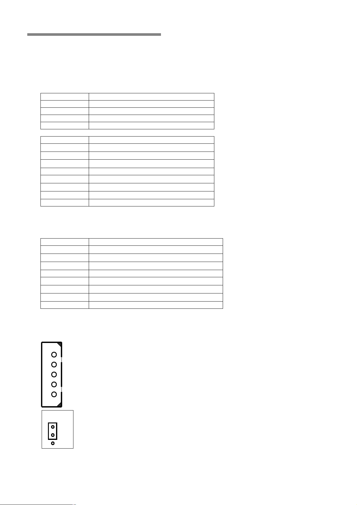
52
15. RS485 Communication
JP6
NO
15.1 RS485 Communication port related parameter
While using serial communication control, this parameter is used to define the BAUD RATE, PROTOCOL and UNIT
NUMBER (or station address).
15.1.1 PDAN series Communication Parameter
Pr.93=PB.ID (P: Protocol, B: Baud Rate,ID: Unit Number):
1. ID is used to assign the communication address while this inverter controlled by RS485 port. ID=01~99
2. P: Protocol
Setting Protocol
P=0 JPS Protocol, parameter number format “nn”
P=1 JPS Protocol, parameter number format “nnn”
P=2 Modbus Protocol, no parity, 8bit binary
P=3 JPS Modbus Protocol, no parity, 8bit binary
3. B: Baud Rate
Setting Baud Rate
B=0
B=1
B=2
B=3 Reserve
B=4
B=5
B=6
B=7 Reserve
4800bps,2stopbits
9600bps,2stopbits
19200bps,2stopbits
4800bps,1stopbits
9600bps,1stopbits
19200bps,1stopbits
15.1.2 PDA/PDE/PDH series Communication Parameter
Pr.93= B.ID (B: Baud Rate, ID: Unit Number):
1. ID is used to assign the communication address while this inverter controlled by RS485 port. ID=01~99
2. B: Baud Rate
Setting Baud Rate
B=0
B=1
B=2
B=3 Reserve
B=4
B=5
B=6
B=7 Reserve
4800bps,7 bit data,Even Parity,2 Stop Bit
9600bps,7 bit data,Even Parity,2 Stop Bit
19200bps,7 bit data,Even Parity,2 Stop Bit
4800bps,7 bit data,Even Parity,1 Stop Bit
9600bps,7 bit data,Even Parity,1 Stop Bit
19200bps,7 bit data,Even Parity,1 Stop Bit
15.2 RS485 Configuration
PDAN series build in RS485 communication port on CON6 of CPU board, the definition of CON6 is:
CON6 (JAM-SC25-05WS)
1:+5V
2: 0V
3:Sig+ (A)
4:Sig- (B)
5:leave this pin open
TR
JP6 jumper of CPU board is used to select with/without Terminal Resistor.
JP1 on TR position, select with Terminal Resistor.
JP1 on NO position, select without Terminal Resistor.
Page 54
53
l RS485 port can use to control multiple inverter by connect the signal in parallel.
l The option of RS485/232 card is used to convert RS485 into RS232.
l The option of standard cable (CABLE_RS485) is used to transform JAM connector (CON6) into standard 9 pin D-
sub Male connector. The definition the D-sub connector is:
9 pin D-sub Male Connector Definition JAM Connector (CON6)
PIN1~3 N.C.
PIN4 A (SIG+) PIN3
PIN5 B (SIG-) PIN4
PIN6 0V PIN2
PIN7~9 N.C.
Note: PDA/PDE/PDH series must use RS485/232 option card when using serial communication control。
15.3 JPS Protocol & Format
All code transfer between Computer and Drive are ASCII code, and the “CR” code (0x0D) must add to the end of each
command string.
Data Format: 7 Bit data,Even Parity。
15.3.1 Computer to Inverter
Computer may send three types of message to drive.
15.3.1.1 Control Command (No response will send back from drive)
Format: “C,uu,cc,fffff”
C: Head of COMMAND String.
uu: ID of drive, from 00 to 99.
If the “uu” code in command string is “00”, all drives can be controlled at the same time.
cc: Control command code, from 00 to 15.
The “cc” number is actually converted from four bits binary data.
cc= 8 * Bit-3 (JOG) + 4 * Bit-2 (Reverse) + 2 * Bit-1 (RUN) + Bit-0 (Reset)
Control Code Function
cc=00 Stop
cc=01 Reset
cc=02 Forward Run
cc=06 Reverse Run
cc=10 Forward JOG Run
cc=14 Reverse JOG Run
fffff: Set Frequency.
PDAN/PDA/PDE series: from 00000 to 65000, representing desired
Hz = 0.00 to 650.00
PDH series: from 00000 to 30000, representing desired
Hz = 0.0 to 3000.0
15.3.1.2 Write Command (No response will send back from drive)
format: “W,uu,nn,ddddd” or “W,uu,nnn,ddddd”
W: Head of WRITE String.
uu: ID of drive, from 00 to 99.
If the “uu” code in command string is “00”, all drives can be controlled at the same time.
nn(n) : PDAN series: If Protocol P=0, Parameter format is “nn”, from 00 to 99
If Protocol P=1, Parameter format is “nnn”, from 000 to 999
PDA/PDE/PDH series: Parameter format is “nn”, from 00 to 99
ddddd : data value, from 00000 to 65535.
If data exceed upper or lower limit (shown in parameter table) will be trimmed within
boundary automatically.
15.3.1.3 Read Command (Drive will send back P-string after receive this string)
Format: “R,uu,nn” or “R,uu,nnn”
R: Head of READ String
uu: ID of drive, from 01 to 99.
Do not specify uu=00 for Read Command while multiple drives are under control.
nn(n) : PDAN series: If Protocol P=0, Parameter format is “nn”, from 00 to 99
If Protocol P=1, Parameter format is “nnn”, from 000 to 999
PDA/PDE/PDH series: Parameter format is “nn”, from 00 to 99
Page 55
54
15.3.2 Drive to Computer
Drive will send back Parameter data and its Status after receive Read Command from computer.
Format: “P,uu,nn,tt,ddddd,s,aaaa” or “P,uu,nnn,tt,ddddd,s,aaaa”
P: P stands for PARAMETER String
uu: ID of drive, from 00 to 99.
This number is defined in Pr.093 of each drive.
nn(n) : PDAN series: If Protocol P=0, Parameter format is “nn”, from 00 to 99
If Protocol P=1, Parameter format is “nnn”, from 000 to 999
PDA/PDE/PDH series: Parameter format is “nn”, from 00 to 99
tt: Data type of this parameter, from 00 to 22.
tt Data Type Data Range Format
0 Read/Write, store in EAROM 00000~65535 999.99
1 Read/Write, store in EAROM 00000~65535 9999.9
2 Read/Write, store in EAROM 00000~65535 99999
3 Read/Write, store in EAROM 00000~00255 999.99
4 Read/Write, store in EAROM 00000~00255 9999.9
5 Read/Write, store in EAROM 00000~00255 99999
6 Read/Write, store in EAROM 00000~00001 99999
7 Read/Write, store in RAM 00000~65535 99999
8 Read only, store in RAM 00000~65535
s: Drive output status, from 0 to 9.
s = 1: Drive Reverse Running
s = 2: Drive Forward Running.
s = 3: Drive Stop
else, undefined.
aaaa: Alarm history, from 0000 to 9999
The drive can record 4 Alarm messages.
Most significant digit stands for oldest Alarm message.
Least significant digit stands for present Alarm message.
Refer to section 14.2 for Alarm code.
9 Read only, store in RAM 00000~65535 999.99
10 Read only, store in RAM 00000~65535 9999.9
11 Read only, store in RAM 00000~65535 99999
12 Read only, store in RAM 00000~00255 999.99
13 Read only, store in RAM 00000~00255 9999.9
14 Read only, store in RAM 00000~00255 99999
15 Read only, store in RAM 00000~00001 99999
16 Read only, store in RAM 00000~00015 99999, (Binary)
17 Read only, store in RAM 00000~00007 99999, (Binary)
18 Read only, store in RAM 00000~00003 99999, (Binary)
19 Read only, store in RAM 00000~01023 99999
20 Read only, store in RAM 00000~00001 99999, (Hex)
22 Read only, store in RAM 00000~00001 99999, (Hex)
ddddd: Data value, from 00000 to 65535.
999.99, if data >32767 which is (65536-ddddd)
15.4 Modbus Protocol
PDAN series: Standard Modbus protocol and JPS Modbus protocol are built in to the inverter as standard, please
contact our application department for details.
Page 56
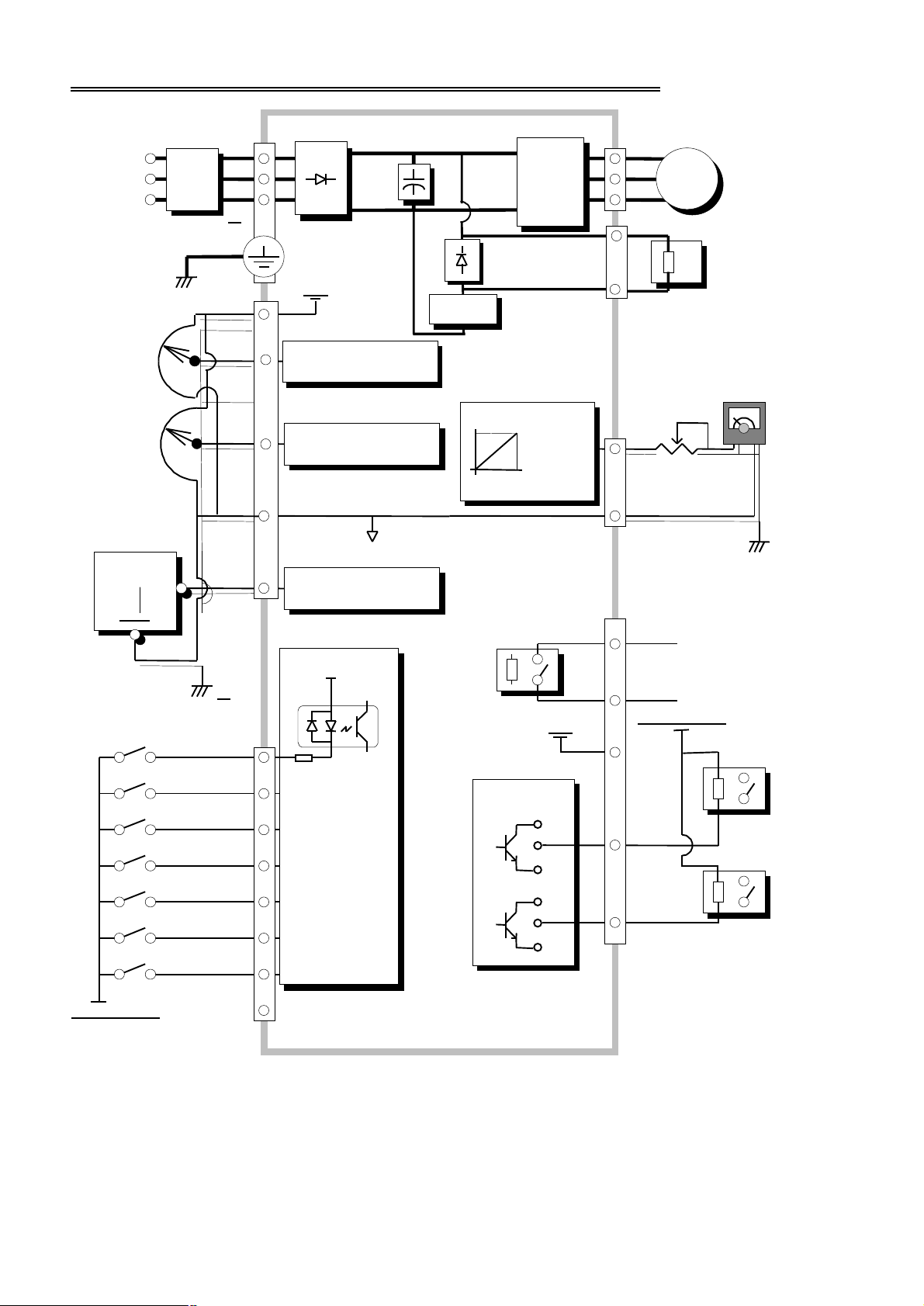
55
16. BLOCK DIAGRAM OF PDA INVERTER
S T E
5V
AM
*2
*4 *4
*5
*5
R
POWER
SOURCE
*1
+5V
BRAKE
POTENTIAL
METER
POTENTIAL
METER
ANALOG
SIGNAL
GND
AI3
AI2
ACOM
AI1
AI3 or PANEL
SELECT BY JP3
V
+5V or 20mA RANGE
SELECT BY JP2
+10V or +5V RANGE
SELECT BY JP1
IGBT
Pr.37
SELECT
U
V
MOTOR
W
P
B or N
ACOM
RY1
*3
*2
MAX. RATING
24VDC, 1A
RY2
24V or DCOM
*6
DI1
DI2
DI3
DI4
RUN
REV
RST
DCOM
PHOTO
ISOLATED
DIGITAL
INPUT PORT
X 7
24V
OPEN
COLLECTER
24V or DCOM
24V
DO1
DO2
MAX. RATING
24VDC, 50mA
*7
Note:
1. Apply NFB before power line input to inverter.
2. The analog signal wires should be shielded & connected to the Earth.
3. Refer to Sec.2.6, in order to select suitable discharging resistor.
4. For models with P & N, must use separate Brake Discharge Unit and do not connect resistor to the P, N terminals
directly.
5. To select Sink (NPN) type or Source (PNP) type by Jumper JP4 & JP5. Refer to section 1.2.3 & 1.2.4.
6. Connect to DCOM if Sink (NPN) type selected; connect to 24V if Source (PNP) type selected.
7. Connect to 24V if Sink (NPN) type selected; connect to DCOM if Source (PNP) type selected
Page 57
56
Appendix A
:
PID Function
The PID function is for PDAN series only.
A-1 PID Parameter
Pr.73 PID Input Select
This parameter composed by “X” & “Y” separated by decimal point, the X value is used to select the PID Set signal
source for PID block, and the Y value is used to select the PID FB signal source for PID block.
The equivalent source for selection value “X” or “Y” is:
Pr.73 Description
0 Constant value defined by Pr.27 (0.00~100.00%)
1
2
3
4
5
6
10 DI2(28) Clock Input, the value calculate as:
Pr.28 PID PID Bias (0.1~100.0%)
Pr.29 PID Boost (0.0~500.0%)
Pr.74 PID Preset (0.1~100.0%)
Pr.75 PID P Gain
Pr.76 PID I Gain
Pr.77 PID D Gain
Note: when use PID block function, do not use other function of Pr.73~77
From Analog Input AI1,0 ~ +5V è 0~0x7FFF
From Analog Input AI2,0 ~ +5V è 0~0x7FFF
From Analog Input AI3,0 ~ +5V è 0~0x7FFF
From Analog Input AI1,+5V ~ 0 è 0~0x7FFF
From Analog Input AI2,+5V ~ 0 è 0~0x7FFF
From Analog Input AI3,+5V ~ 0 è 0~0x7FFF
0x7FFF * (Clocks Input from DI2(28) per 13.2ms / Pr.71)
A-2 Digital Input Function
DIx Function Description
50 PID Enable If DIx(50) = OFF, PID block disabled.
If DIx(50) = ON, PID block enabled.
51 PID Hold If DIx(51) = OFF, PID Integrator normal.
If DIx(51) = ON, PID Integrator Hold.
52 PID Clear If DIx(52) = ON, PID Integrator Clear.
53 PID Preset If DIx(53) = ON, PID Integrator preset to the value defined by Pr.74
54 PID Bias Enable If DIx(54) = ON, Bias = Bias Input Enable.
If DIx(54)=OFF, Bias = 0
55 PID Boost Enable If DIx(55) = ON, Boost = Pr.29 (0.0~500.0%)
If DIx(55) = OFF, Boost = 100.0%.
when DIx(55) = ON, PID output will hold on original value, it is
similar to DIx(51)
A-3 Speed Source
Pr.40 Speed Source
40 Set Frequency = PID Output
48 If DIx(54) = ON, Set Frequency = (PID Boost * (PID Output + Bias Input from AI1))
If DIx(54) = OFF, Set Frequency = (PID Boost * PID Output)
49 If DIx(54) = ON, Set Frequency = (PID Boost * (PID Output + Bias Input from AI2))
If DIx(54) = OFF, Set Frequency = (PID Boost * PID Output)
50 If DIx(54) = ON, Set Frequency = (PID Boost * (PID Output + Bias Input from AI3))
If DIx(54) = OFF, Set Frequency = (PID Boost * PID Output))
51 If DIx(54) = ON, Set Frequency = (PID Boost * (PID Output + Bias Set by Pr.28))
If DIx(54) = OFF, Set Frequency = (PID Boost * PID Output
A-4 Analog Function
Pr.37 AM Output
7 PID Output
8 If DIx(54) = ON, AM = +5V * (PID Boost * (PID Output + Bias Input from AI1))
If DIx(54) = OFF, AM = +5V * (PID Boost * PID Output)
9 If DIx(54) = ON, AM = +5V * (PID Boost * (PID Output + Bias Input from AI2))
If DIx(54) = OFF, AM = +5V * (PID Boost * PID Output)
10 If DIx(54) = ON, AM = +5V * (PID Boost * (PID Output + Bias Input from AI3))
If DIx(54) = OFF, AM = +5V * (PID Boost * PID Output)
11 If DIx(54) = ON, AM = +5V * (PID Boost * (PID Output + Bias Set by Pr.28))
If DIx(54) = OFF, AM = +5V * (PID Boost * PID Output)
Page 58
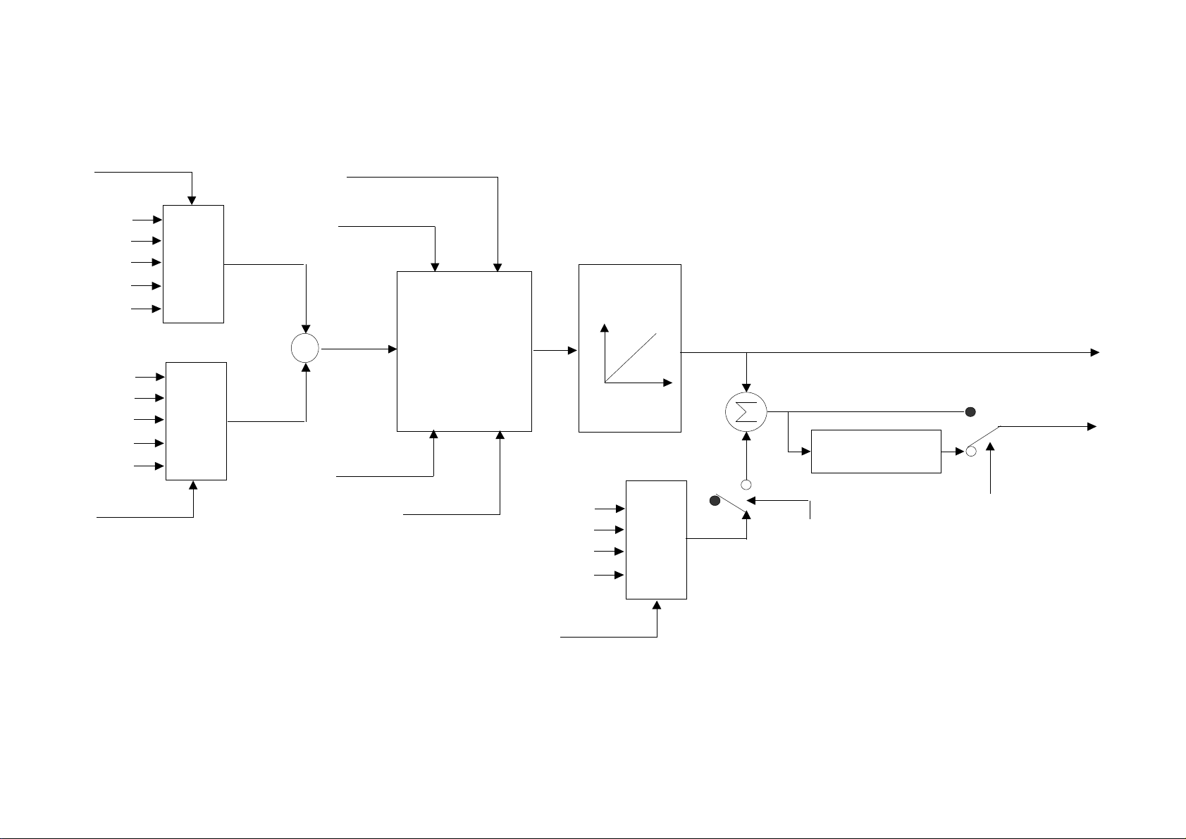
57
A-5 PID Function Block
-
Set Selection (X)
PID Integrator Clear DIx(52)
Pr.27
AI-1
AI-2
AI-3
DI-2
Pr.73=X.Y
Pr.27
AI-1
AI-2
AI-3
DI-2
FB Selection (Y)
Switch
Switch
PID SET
+
PID FB
PID Integrator Hold DIx(51)
PID Process
ERROR
Σ
PID Enable DIx(50)
PID Preset DIx(53)
Preset(Pr.74)
P Gain(Pr.75)
I Gain(Pr.76)
D Gain(Pr.77)
D Time=200ms
Pr.28
AI-1
AI-2
AI-3
+
Switch
PID Output
PID Output
PID + Bias Output
Gain=Pr.29/100.0
Boost Enable DIx(55)
Bias Enable DIx(54)
Bias Select
Page 59

JPS
JOINT PEER SYSTEC CORP.
() 1R/Q6HF=KRQJKH6WQGIORRU
;LQVKH'LVW7DLFKXQJ&LW\7DLZDQ
TEL: 886--26866 FAX: 886--24889
http://www.jps.com.tw
E-mail: MSV[email protected]
 Loading...