

Page 1

COPYRIGHT
The copyright in programs entered in this machine is
exclusively the property of JPM (Automatic Machines) Limited.
Copyright on all illustrated panels and artwork is also exclusively
the property of JPM (Automatic Machines) Limited.
Copying or any other form of transferring of any program or
artwork thereof from any such machine to any other machine is
expressly forbidden without the written authority ofthe Company.
JPM (Automatic Machines) Ltd.
Hadfield Road, Leckwith Trading Estate.
South Glamorgan, CF1 8AQ. Cardiff ,
Telephone 0222-223000
Telex 497806. Fax 0222238214.
Page 2

2
Page 3

3
MPS2 SYSTEM Contents
page
INSTALLATIONPROCEDURE 1
INTRODUCTION 2
SYSTEM CAPABlLITIES 3-4
POWERSUPPLY-ELECTRICALSPECIFICATION 5-6
POWER SUPPLY CONNECTOR DETAILS. 7
PRINCIPLE OF MULTIPLEXED LAMP SYSTEM 8
MULTIPLEXING-TECHNICAL DESCRIPTION 9
MS111 MULTI COINACCEPTOR TOP ENTRY& SIDE ENTRY 10
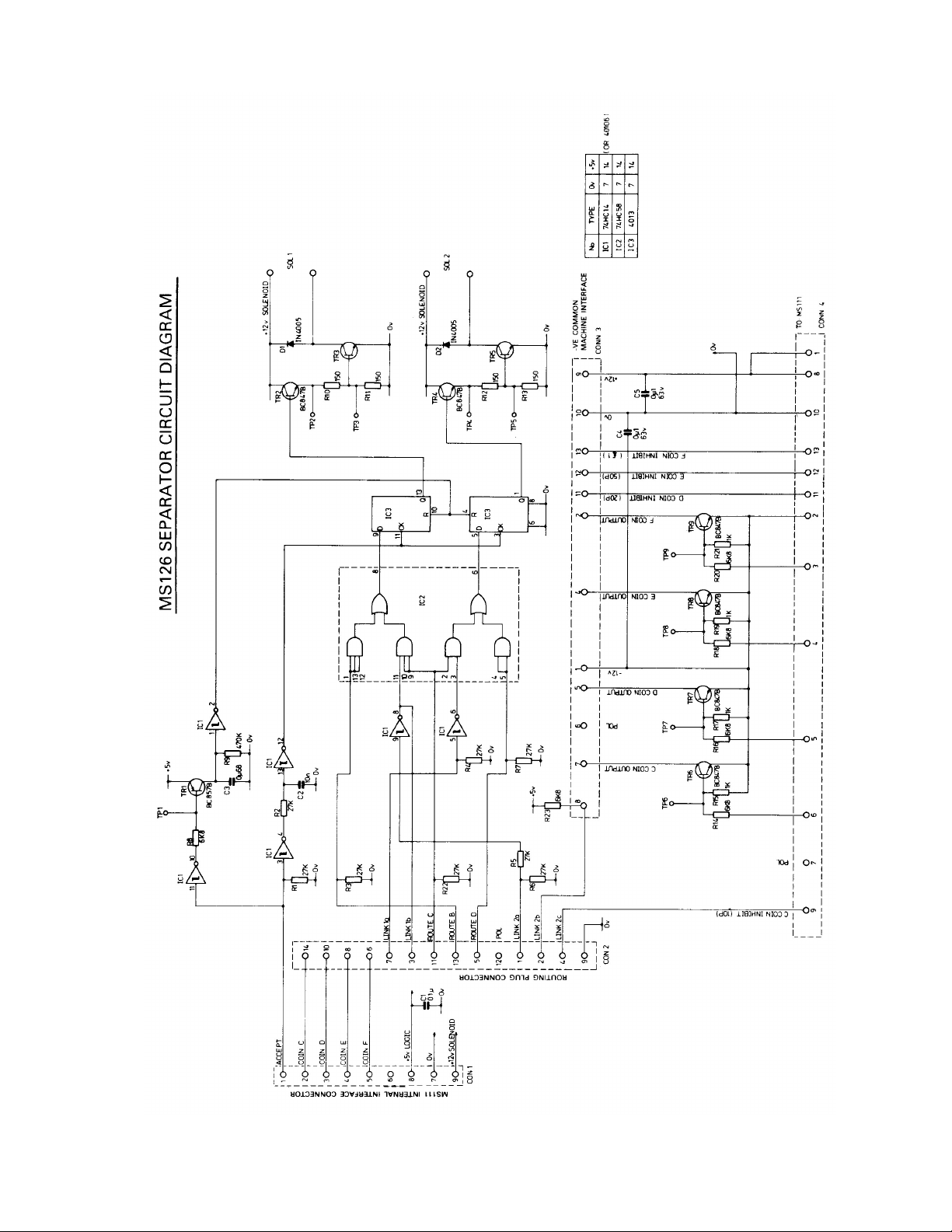
MS126 SEPARATOR 11
MS126 ROUTING CONFIGURATION 12-13
MS126 SEPARATOR CIRCUITDIAGRAM 14
MAIN BOARD - TECHNICAL DESCRIPTION 15-20
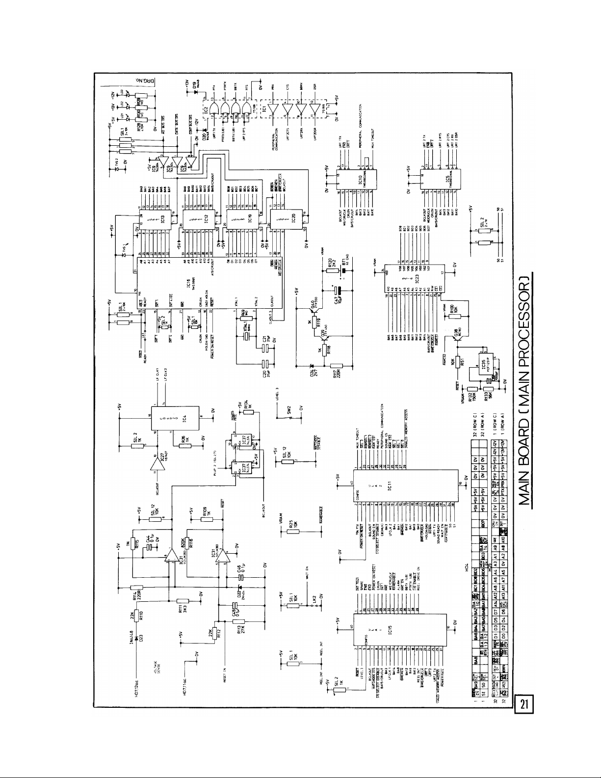
MAIN BOARD - MAIN PROCESSOR CIRCUIT DIAGRAM 21
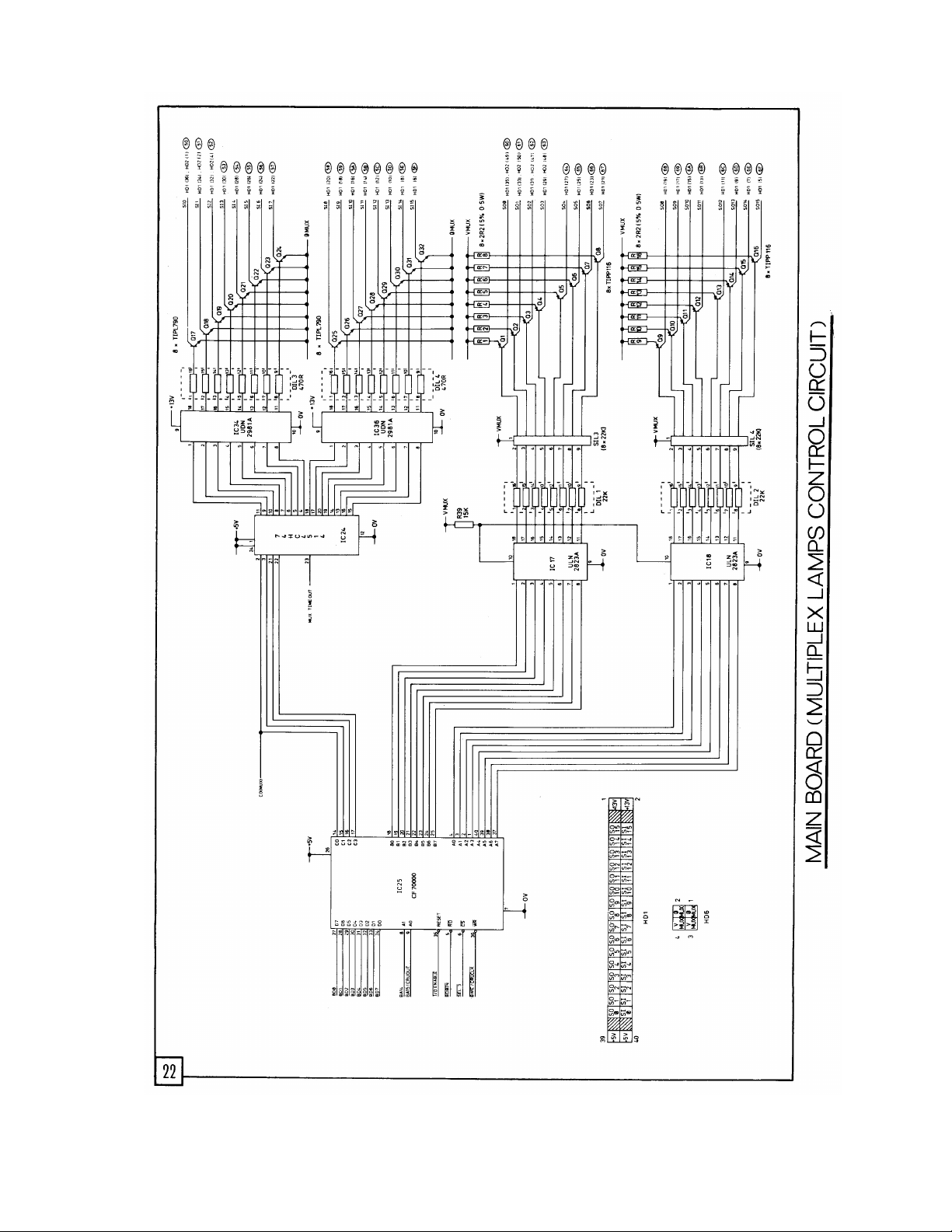
MAIN BOARD - MULTIPLEXER CIRCUIT DIAGRAM 22
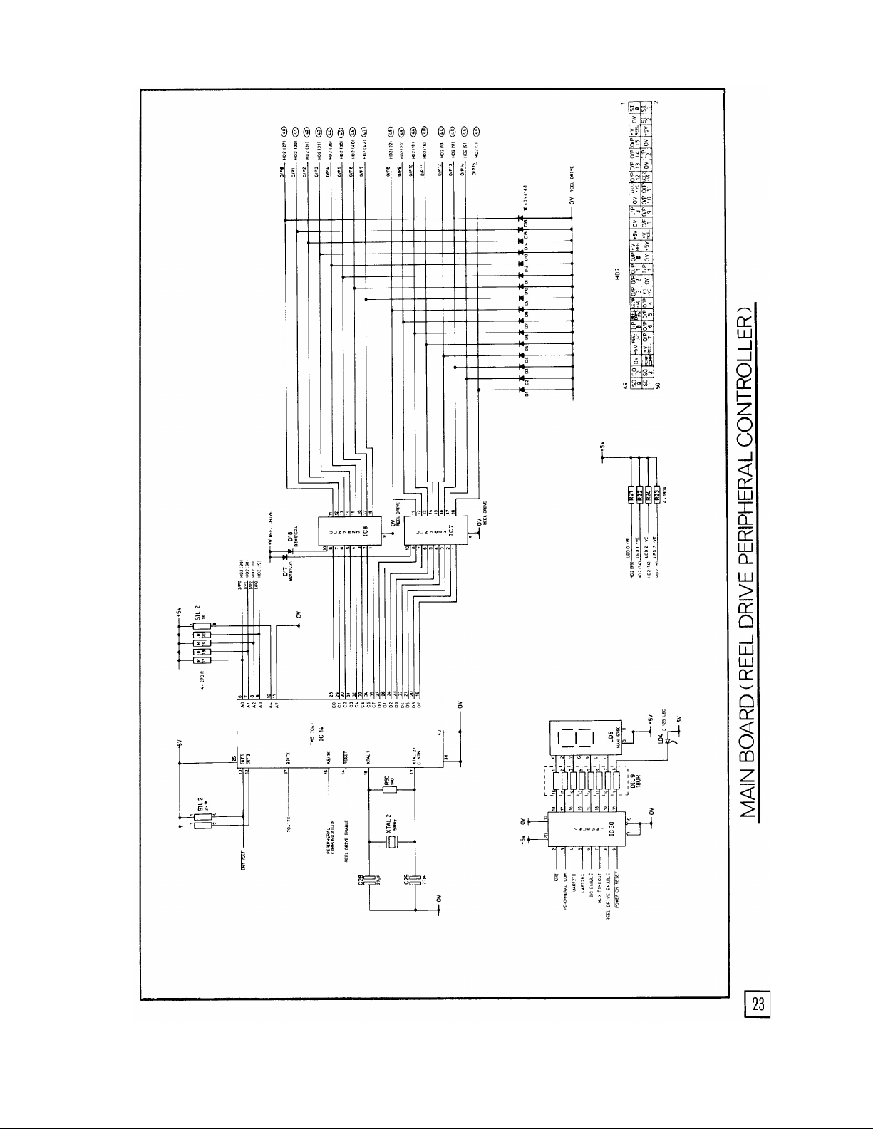
MAIN BOARD – REEL DRIVE PERIPHERAL CONTROLLER CIRCUIT DIAGRAM. 23
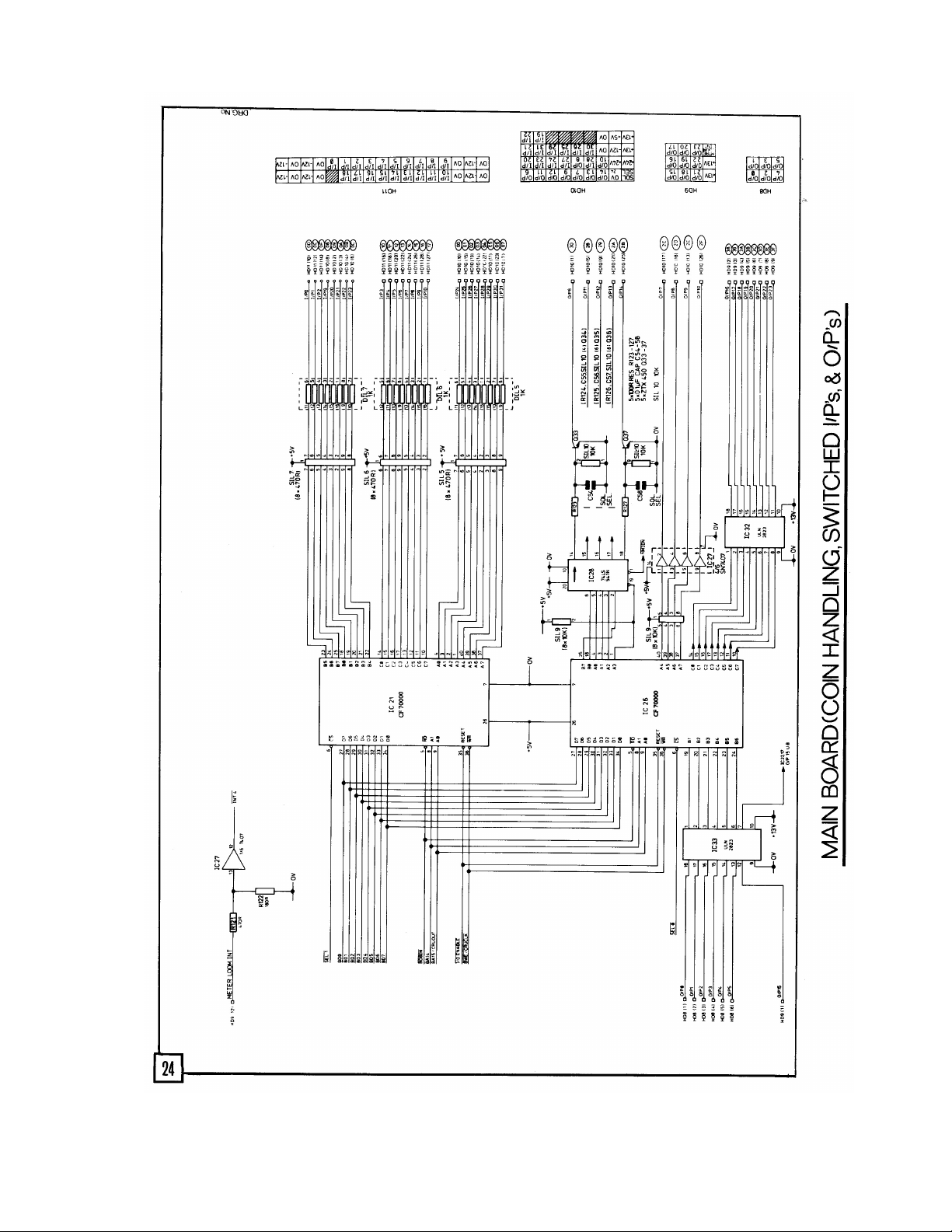
MAIN BOARD - COIN HANDLING, SWITCHED I/P'S & O/P'S CIRCUIT DIAGRAM. 24
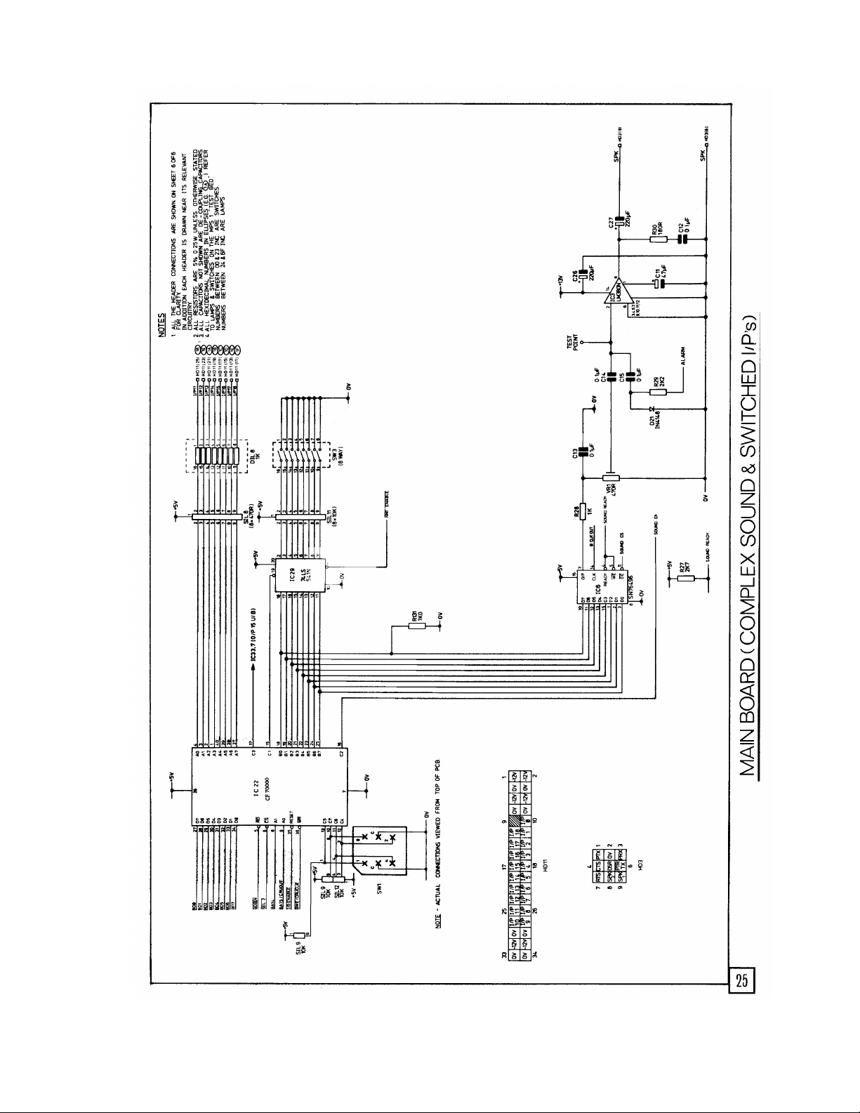
MAIN BOARD - COMPLEX SOUND AND SWITCHED INPUTS DIAGRAM. 25
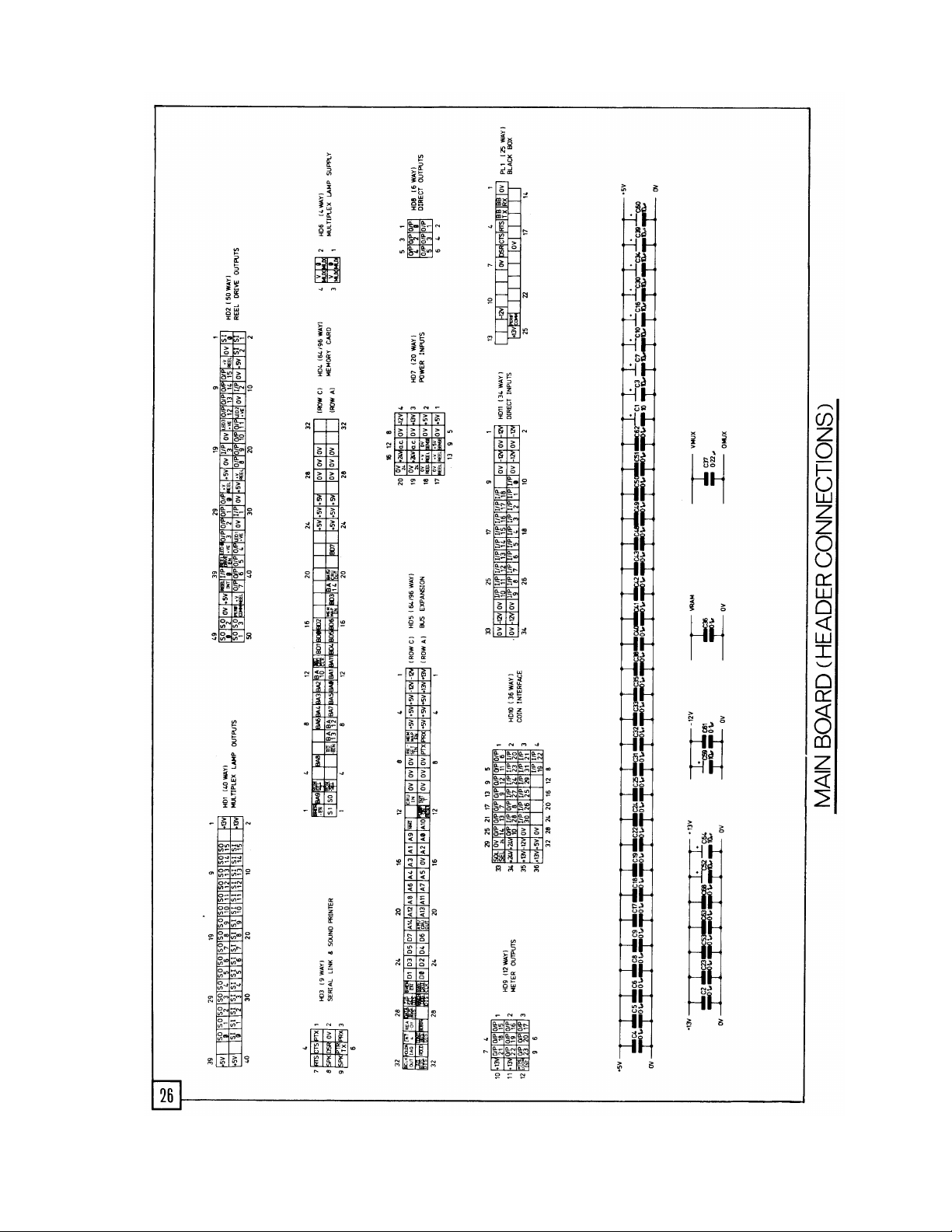
MAIN BOARD – HEADER CONNECTIONS DIAGRAM 26
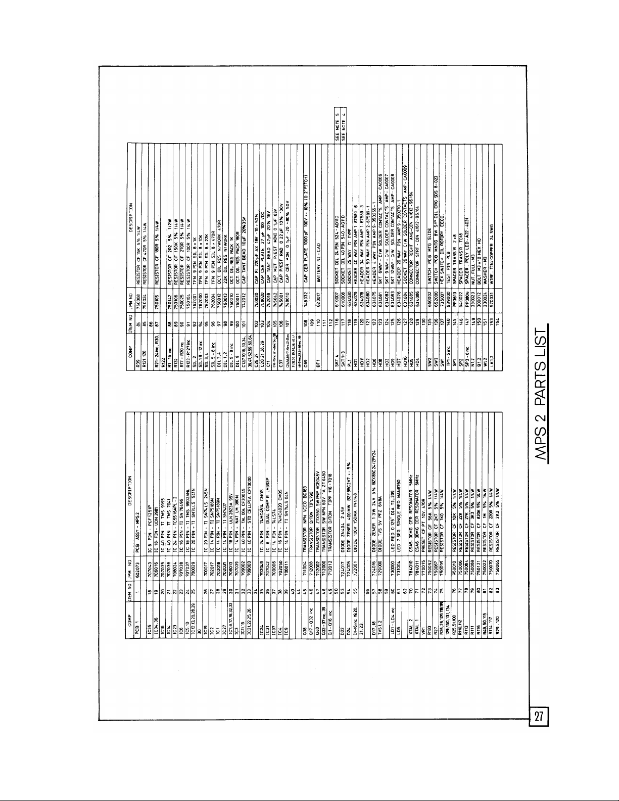
MAIN BOARD PARTSLIST 27
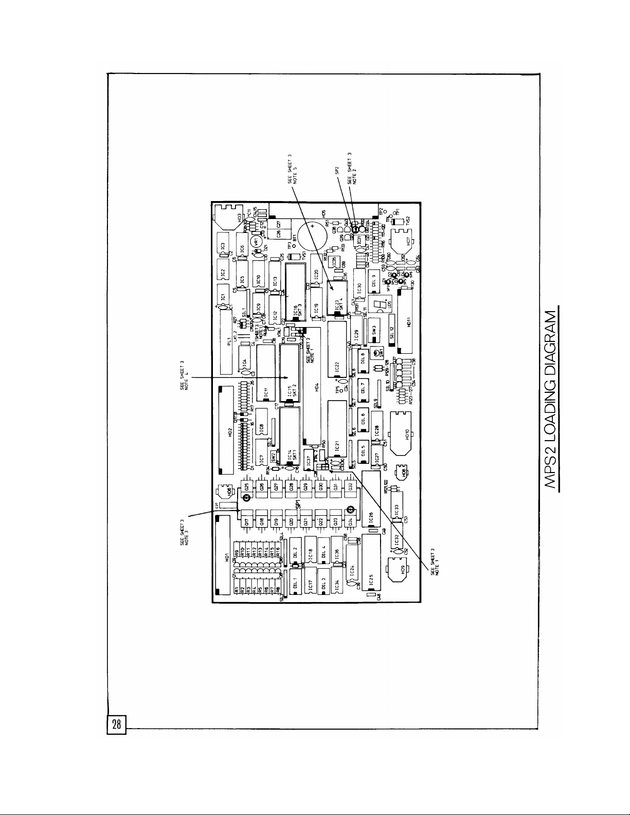
MAIN BOARD LOADING DIAGRAM. 28
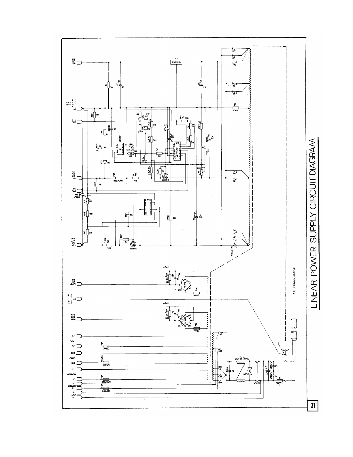
LlNEAR POWER SUPPLY - TECHNICAL DESCRIPTION 29-30
LlNEAR POWER SUPPLY - CIRCUIT DIAGRAM 31
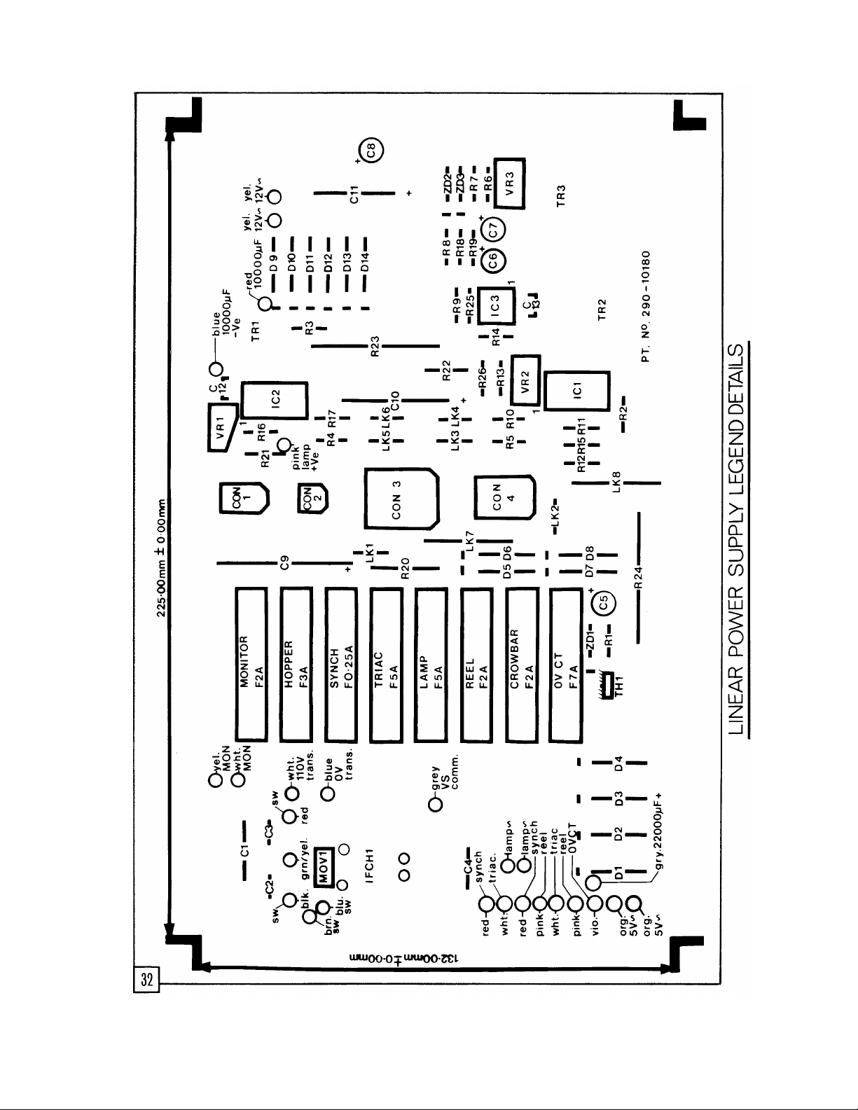
LlNEAR POWER SUPPLY - LOADING DIAGRAM 32
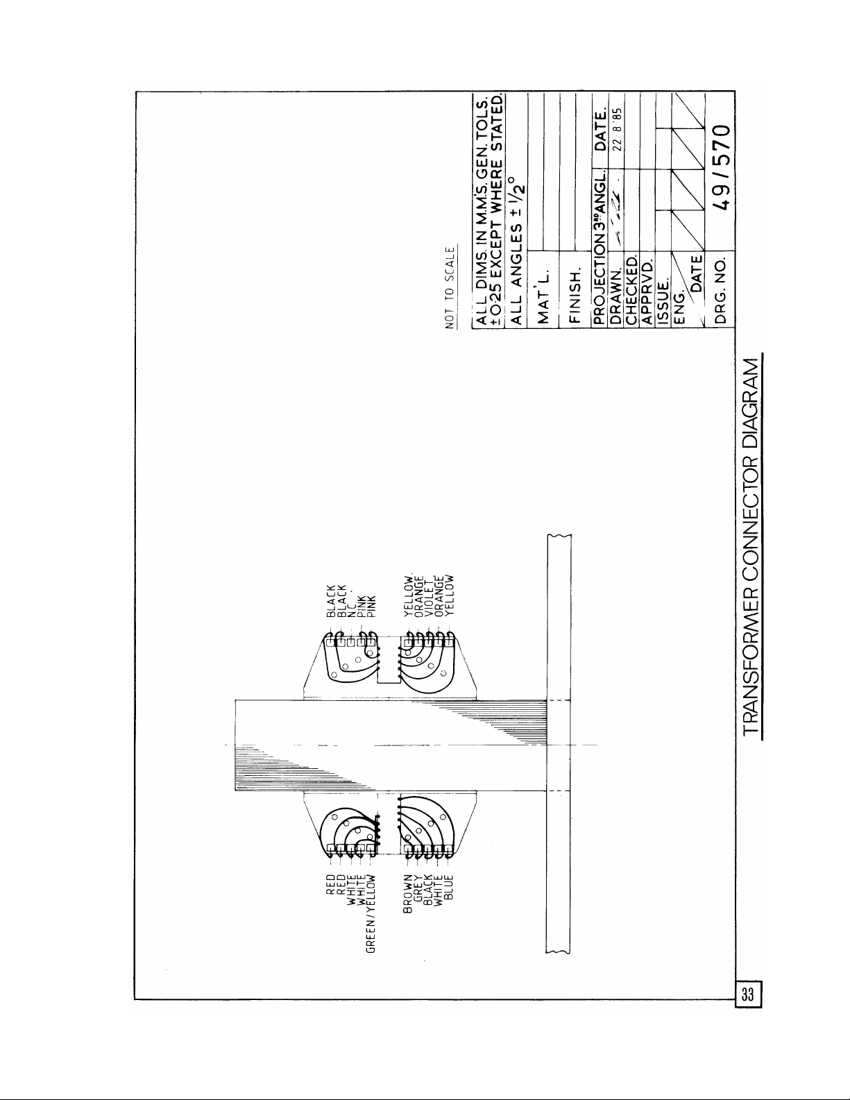
LlNEAR POWER SUPPLY - TRANSFORMER COLOUR CODE. 33
LlNEAR POWER SUPPLY - PARTSLIST 34
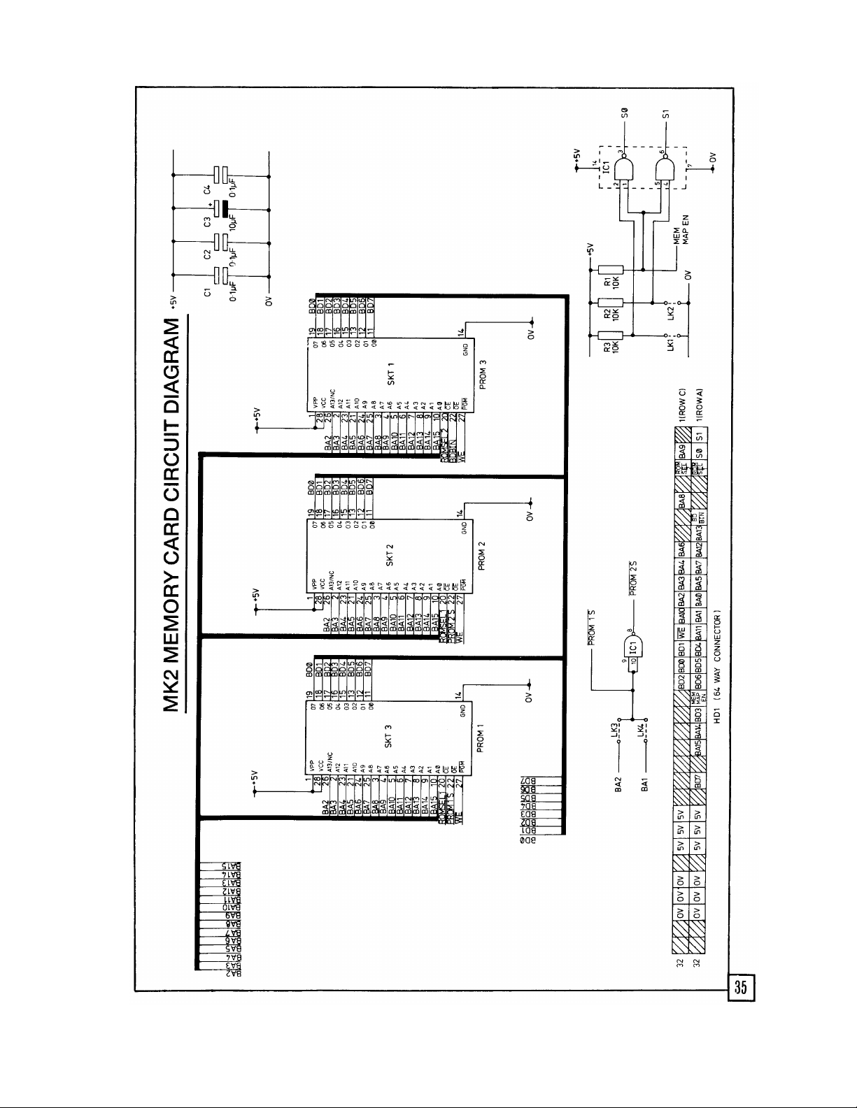
MK2 MEMORY CARD – CIRCUIT DIAGRAM 35
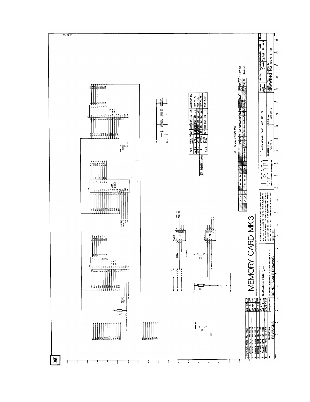
MK3 MEMORY CARD – CIRCUIT DIAGRAM 36
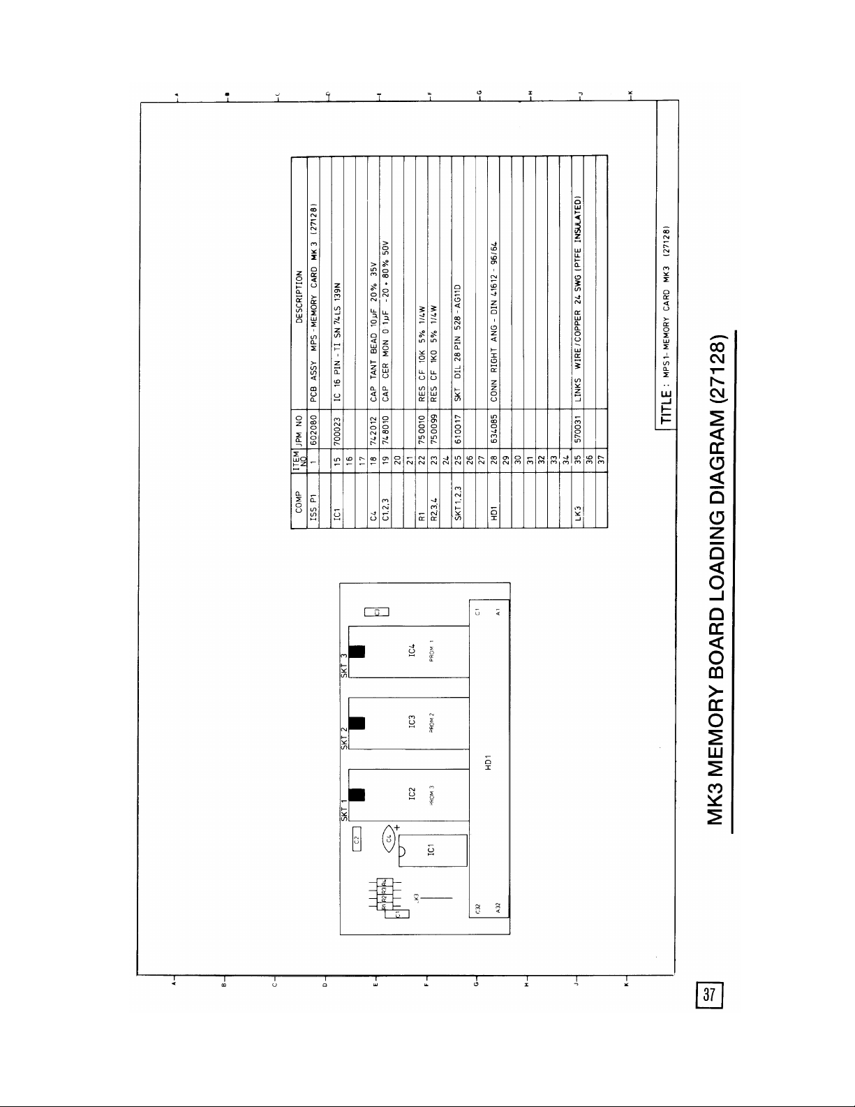
MK3 MEMORY BOARD - LOADING DIAGRAM (27128) 37
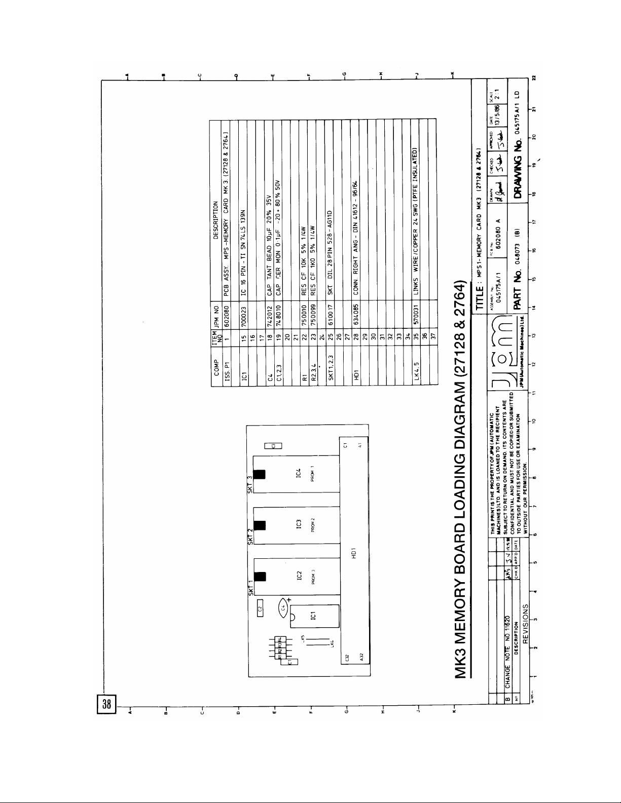
MK3 MEMORY BOARD - LOADING DIAGRAM (27128 & 2764) 38
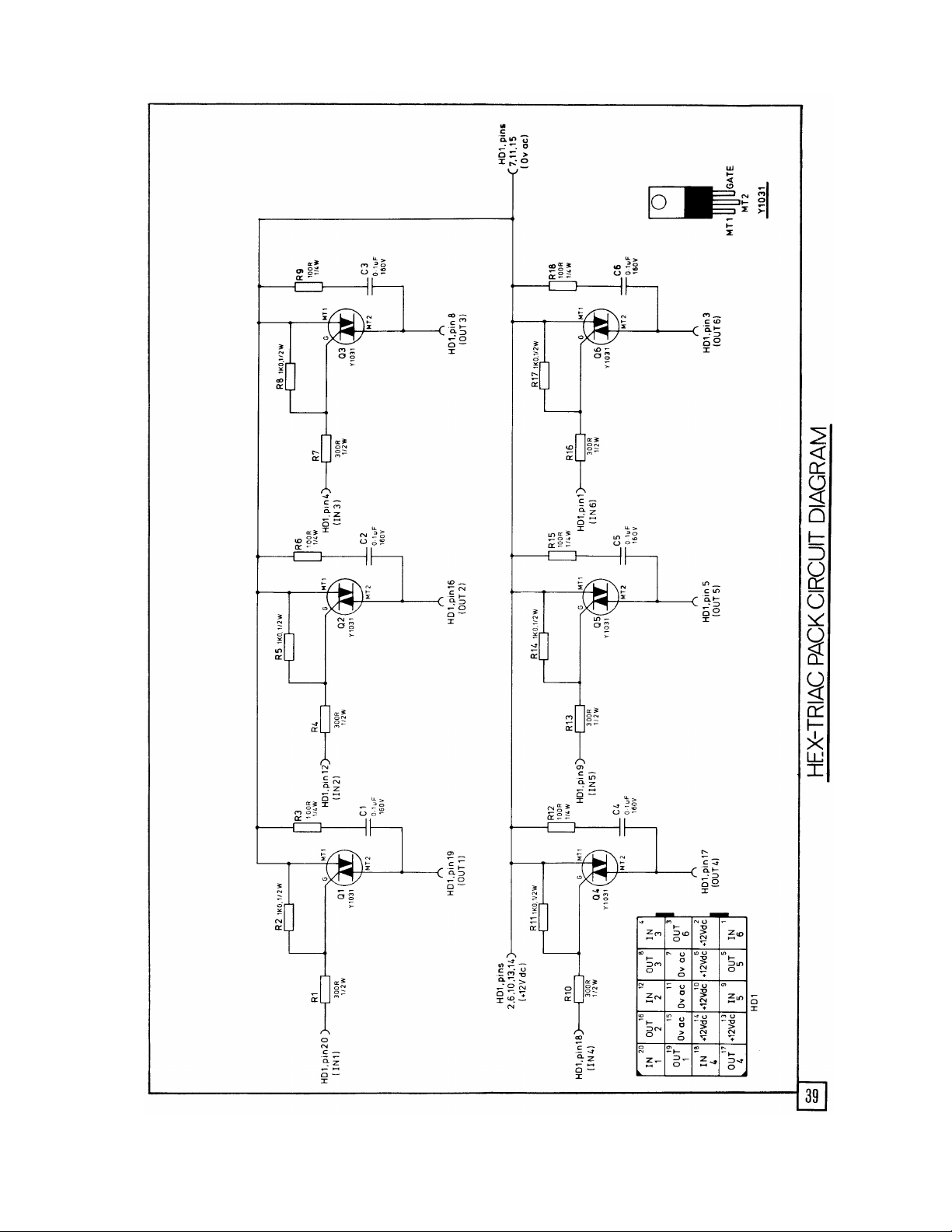
HEX TRIAC PACK - CIRCUIT DIAGRAM 39
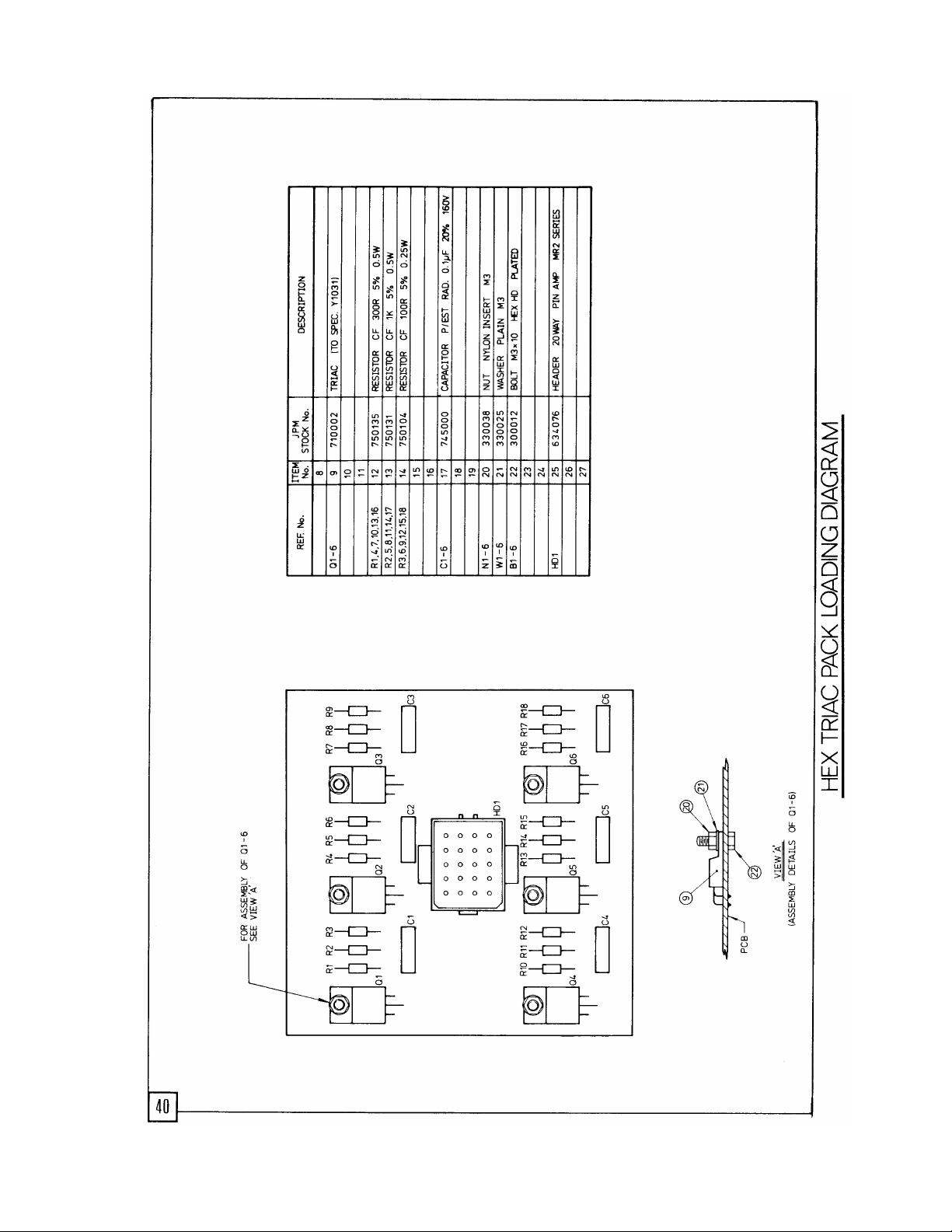
HEX TRIAC PACK – LOADING DIAGRAM 40
15 DIGIT DRIVER BOARD - TECHNICAL DESCRIPTION. 41
15 DIGIT DISPLAY BOARD – TECHNICAL DESCRIPTION. 41
2 DIGIT DISPLAY BOARD – TECHNICAL DESCRIPTION. 41
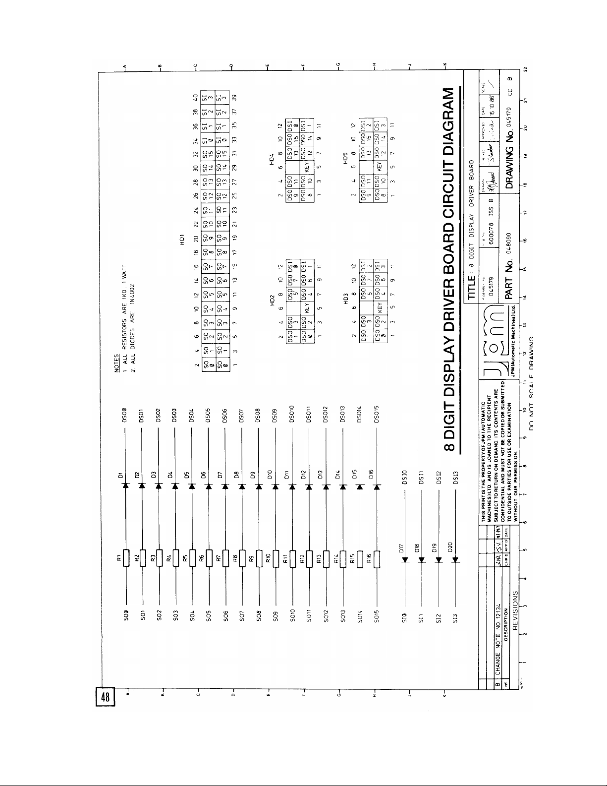
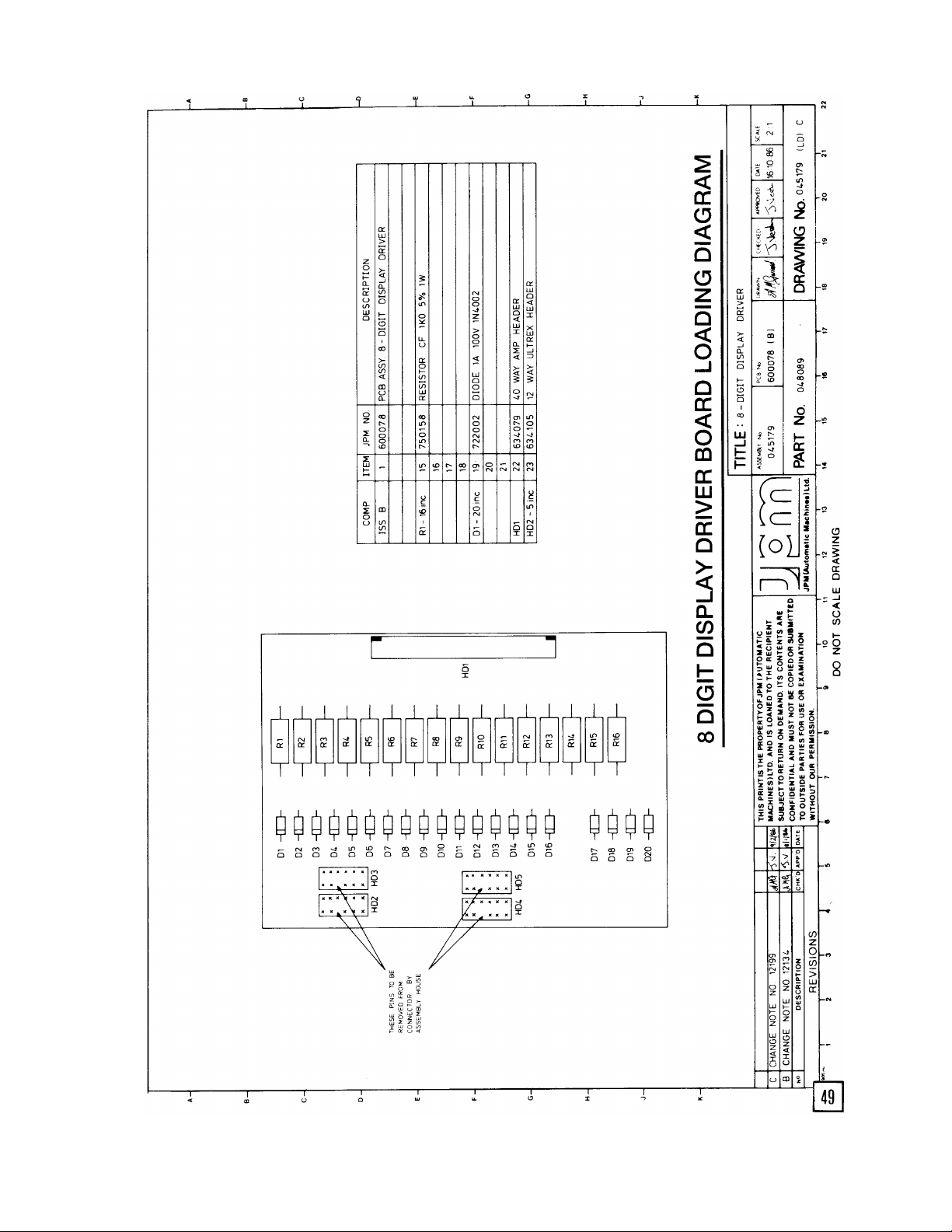
8 DIGIT DISPLAY DRIVER BOARD - TECHNICAL DESCRIPTION 41
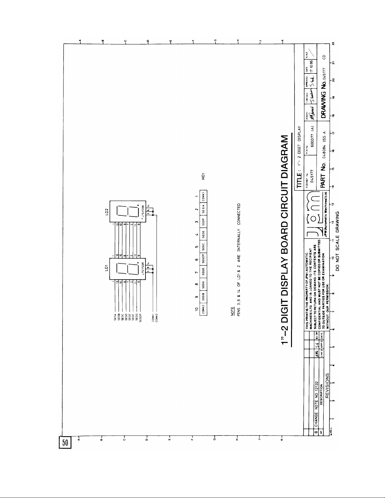
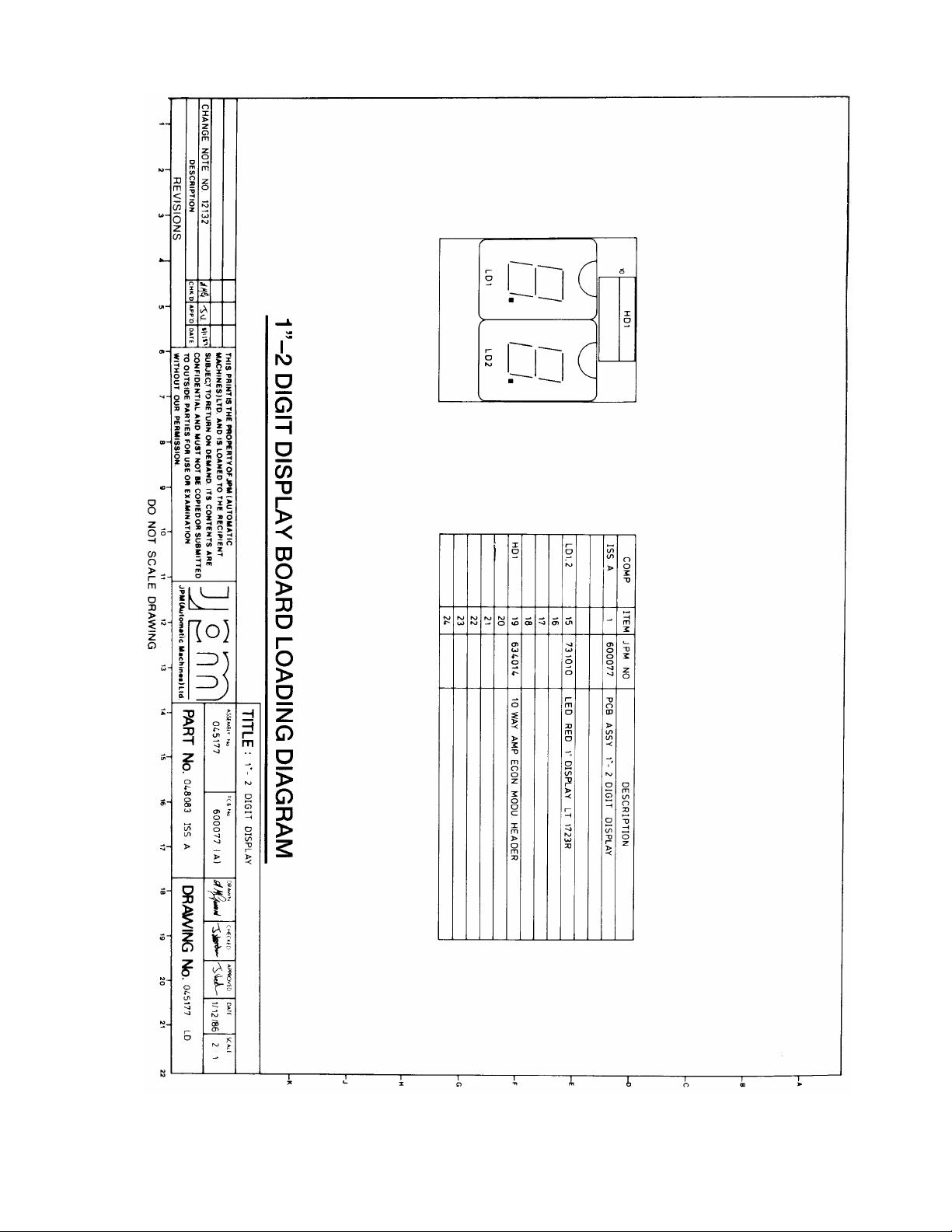
1" - 2 DIGIT DISPLAY BOARD – TECHNICAL DESCRIPTION 41
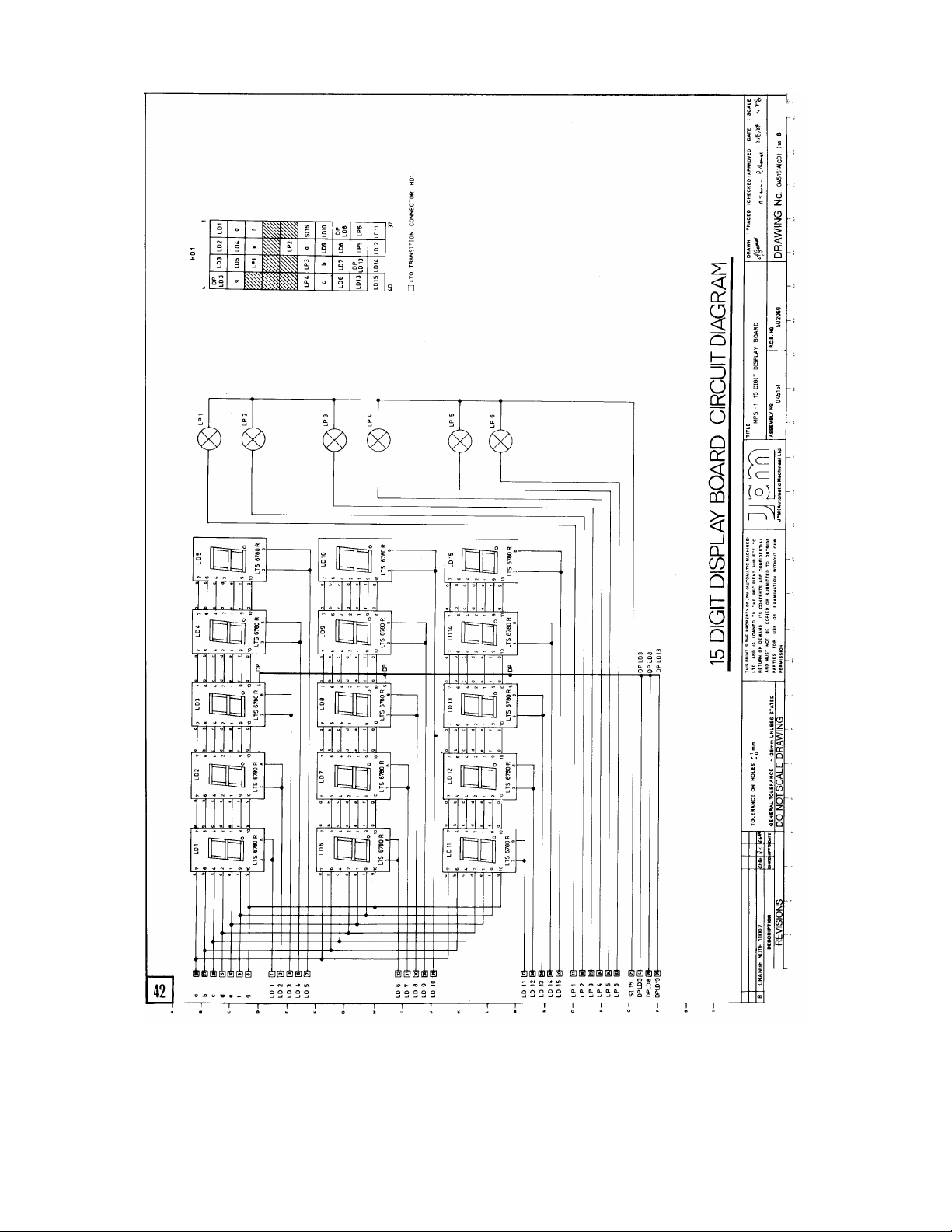
15 DIGIT DISPLAY BOARD – CIRCUIT DIAGRAM 42
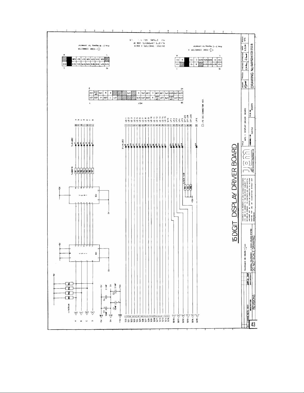
15 DIGIT DISPLAY DRIVER BOARD - CIRCUIT DIAGRAM 43
15 DIGIT DISPLAY DRIVER BOARD - LOADING DIAGRAM. 44
15 DIGIT DISPLAY BOARD – LOADING DIAGRAM 45
2 DIGIT DISPLAY BOARD - CIRCUIT DIAGRAM 46
2 DIGIT DISPLAY BOARD – LOADING DIAGRAM 47
8 DIGIT DISPLAY DRIVERBOARD - CIRCUITDIAGRAM 48
8 DIGIT DISPLAY DRIVERBOARD - LOADINGDIAGRAM 49
1" - 2” DIGIT DISPLAY BOARD - CIRCUIT DIAGRAM 50
1" - 2” DIGIT DISPLAY BOARD – LOADING DIAGRAM 51
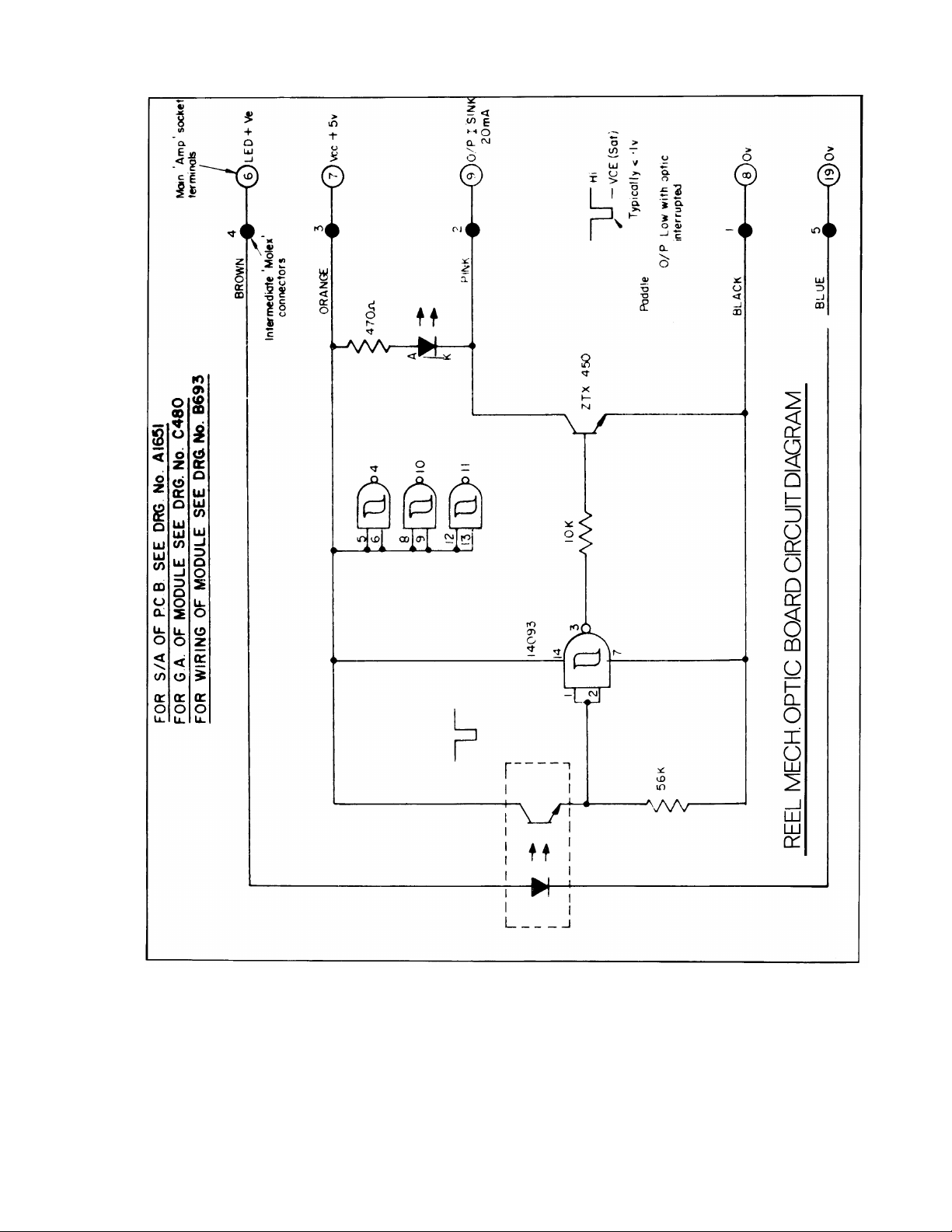
REEL MECH OPTIC BOARD – CIRCUIT DIAGRAM 52
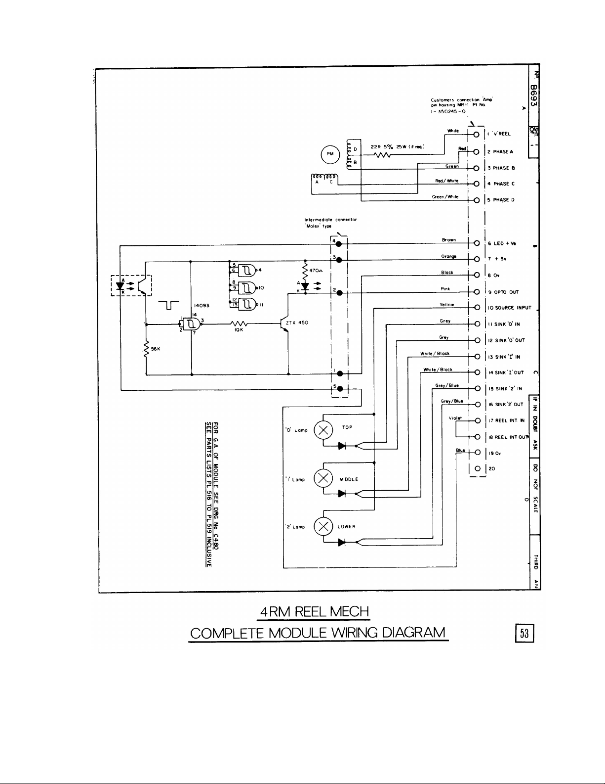
4RM REEL MECH COMPLETE MODULE WIRINGDIAGRAM 53
WARRANTY 54
MPS2 based machines are designed and built to take advantage of the system capabilities. As such, servicing and repairs
should Only be carried out by trained personnel. Modifications to assemblies should not be undertaken except as and when
detailed by J.P.M. (Automatic Machines) Limited.
Page 4
MPS2 INSTALLATION PROCEDURE
Installation Procedure
1. Ensure that all plugs and sockets are engaged, also that all earth connections are secure.
2. Connect to mains supply and switch on at the transformer assembly.
3. During power up, a tone will sound and the power on reset LED on the main board will illuminate for
approximately 3 seconds then extinguish.
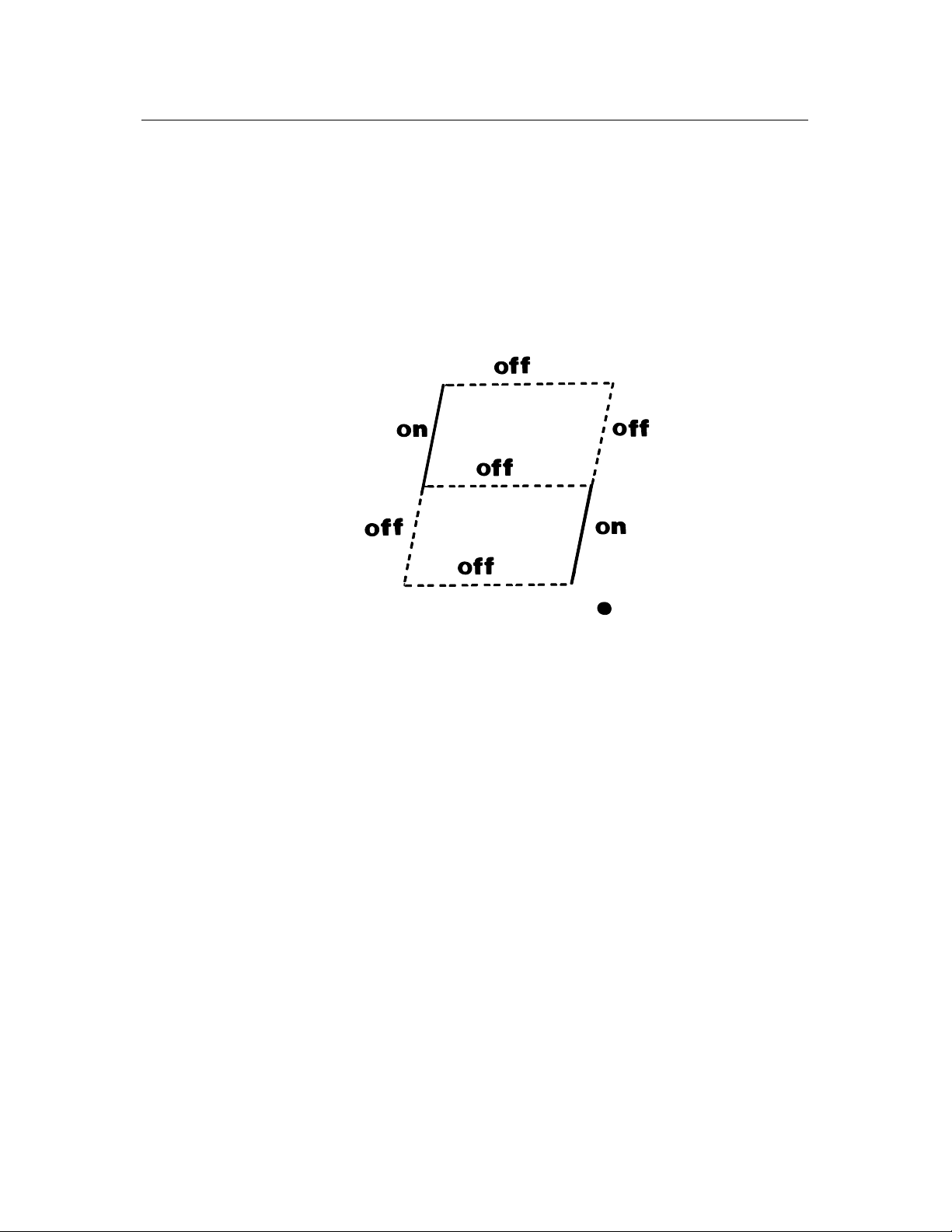
4. For correct operation, the following segments of diagnostic LED 5 will illuminate.
The power supply LED's 1 -3 (+5v, +12v, -12v) should also be illuminated.
5. After the initial reel spin you may proceed with the self test routine as detailed in the personality package.
The function of each individual segment is as follows:
TOP UART2 TX ON = Transmit Data.
TOP LEFT I/O Enable ON = Enable.
TOP RIGHT UART2 RX ON = Receive Data.
CENTRE NM1 ON = Interrupt State.
BOTTOM LEFT Reel Drive Enable OFF = Enable.
BOTTOM RIGHT MUX Timeout OFF = Timeout.
BOTTOM Peripheral Communication ON = Transit Data.
DECIMAL POINT Not Used
Mains Input
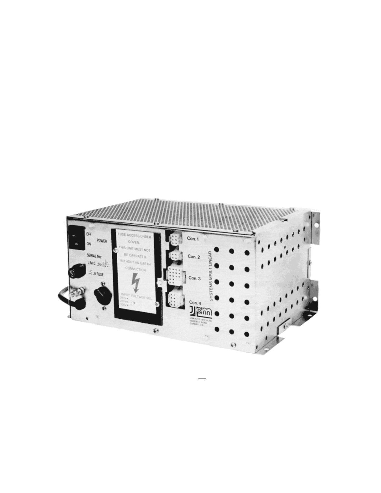
The mains transformer has the facility to be operated from 200v, 220v or 240v AC input. This is achieved via a
plug fitted to the exterior of the chassis. The plug is polarised and can in no way be inserted incorrectly. For
connector details see label on power supply chassis.
Page 5

2
INTRODUCTION
Since the introduction of MPS1 , J.P.M. have decided to keep in line with technical advances and following their
continuous policy of improvement to introduce MPS2.
The MPS2 PCB is electronicaily compatible with the MPS1 PCB. The PCB is mounted in a moulded plastic
enclosure of the same size as the MPS1 PCB, thus making both units retrofittable. Cut-outs are provided for the
memory PCB and the bus interface connector .
As with the MPS2 main board, the new Linear PSU is completely compatible with the MPS1 power supply as
well as being especially designed for MPS2 machines.
The new power supply is designed to aid service engineers in the repair of J.P.M. machines.
This service manual should enable the field service engineer to ensure that the MPS2 machine is installed and
operating correctly, and also to assist him locate and correct any faults that may occur. It will also assist the more
technically minded workshop engineer via the circuit diagrams and the detailed explanation of the various
electronic circuits.
Note
The information contained in this manual, which remains the property of J.P.M. (Automatic Machines) Limited,
is loaned solely for the purpose of operating, maintaining and repairing J.P.M. equipment and may not be used
by, or loaned to, any person for any other reason. Neither may it, or any part thereof, be copied or reproduced by
any means or for any purpose, other than with the express permission of J.P.M. (Automatic Machines) Limited.
J.P.M. (Automatic Machines) Limited reserves the right to make any alterations to components and/or values
where necessary to conform to their policy of continuous product improvement and to keep pace with
technological advancement.
Page 6

3
SYSTEM CAPABILITIES
Sound Generation
Complex Sound Generation utilising the TI SN 76489. The power output is 2W into 8 Ohms. There is on board
volume control, capable of being by-passed by the alarm signal.
Serial Communication
This is achieved via the RS 232 interface.
Data Storage
This is achieved by 2K bytes (expanding to 8K x 8) Cmos RAM. Battery back up is provided by an on board rechargeable NI-CAD battery with a 5 year life.
On Board Switches
The following are provided:
1 off - Hexidecimal rotary switch (0 to F).
1 off - 8 way SPST DIL switch.
MK 3 Memory Board
The memory board consists of three 28 pin sockets and an IC for address decoding. The IC (74LS139N)
provides additional address to that already present on the MPS1 and MPS2 main boards. The three 28 pin
sockets can take either 8K x 8 (2764), 16K x 8 (27125) or 32K x 8 (27256) EPROM's, giving the memory board
a capacity of between 24K (3 x 2764's), 48K (3 x 27128's) or 48K (1 x 27256 and 1 x 27128).
The decoding for these types of EPROM's is selectable by links 1 to 5 on the Memory card:
For 3 x 2764, links 4 and 5 inserted.
For 2 x 2764 and 1 x 27128, links 4 and 5 inserted.
For 3 x 27128, link 3 inserted.
For 1 x 27256, links 1 and 2 inserted.
Power Supply
The supplies for MPS2 are of the linear variety and include.
a) +5v at 1.5 A.
b) +12v DC at 1.8A.
c) -12v DC at 0.2A.
Unregulated supplies are:
1) 50v DC at 5A Lamps Supply (VMUX).
2) 24v DC at 1 A Reel Supply.
3) 50v AC at 2.5A AC payout solenoids.
4) 110v AC at 1.3A Hopper Supply.
5) 48v AC peak at 100mA - Low Mains Supply Sensor .
6) 128v AC at 1 A -Video Monitor Supply.
For further information on specification of power supply see pages 5 & 6.
Page 7

4
SYSTEM CAPABILITIES
OUTPUTS
Multiplexed
There are 256 multiplexed outputs in a 16 x 16 array. Sources 0 to 15. Sinks 0 to 15 connector HD1. Each output
is capable of driving a 1 w lamp at a supply of 50v DC in a 12.5% dut y cycle.
Reel Drives
There are sixteen dedicated reel drive outputs (0 to 15) connector HD2, each capable of driving 500mA at a
maximum pulse rate of 400 half steps per second.
Coin Inhibits
There are four T.T.L. outputs, output 7 to output 10 connector HD10, to operate electronic coin acceptor inhibits.
There are five open collector outputs, output 6 and output 11 to output 14, connector HD10, to operate
electromechanical AC solenoids via a triac.
Meters
There are nine meter drives, output 15 to output 23 connector HD9, each capable of sinking 1 A at 40v.
Direct Drives
There are six outputs, output 0 to output 15 connector HD8, capable of sinking 1A at 40v.
INPUTS
Reel Sensor Inputs
There are four dedicated inputs, input 0 to input 3 connector HD2, communicating directIy with the reel drive
processor.
Direct Inputs
There are nineteen inputs, input 0 to input 18 connector HD11 , each capable of sinking 10mA.
Coin Inputs
One input, input 20 HD20, is configured for microswitch use.
Inputs 21 to 24 connector HD1 0 are used for electronic coin accept signals.
Low Level Detector Inputs
Inputs 25 to 28 connector HD10 capable of sinking 10mA.
Non Payout Detector Inputs
Inputs 29 to 32, HD10 capable of sinking 10mA.
Page 8

5
POWER SUPPLY -ELECTRICAL SPECIFICATION
REGULATED LINEAR OUTPUTS
Logic Supply
Voltage - +5v DC.
Current - 1.5 A continuous
Ripple - 50mV peak to peak. (max)
Tolerance - 4.75v to 5.25v.
Crowbar - 6.8v Max.
RS232 Coin Acceptor and Sound Supply
Voltage - +12vDC.
Current - 1.8 A continuous
Ripple - 100mV peak to peak. (max)
Tolerance - 11.4v to 12.6v.
Switch Bias Supply
Voltage - -12vDC.
Current - 0.2 A continuous
Ripple - 100mV peak to peak. (max)
Tolerance - -11.4v to 12.6v.
UNREGULATED SUPPLIES
Lamp Supply VMUX
Voltage - +50vDC.
Current - 0.5 A continuous 5A peak.
Ripple - 5v peak to peak. (max)
Tolerance - +45 to +55v.
Reel Supply VREEL
Voltage - +24vDC.
Current - 1A continuous
Ripple - 5v peak to peak. (max)
Tolerance - 21v to 27v.
Triac Supply VTRIAC
Voltage - 50v AC.
Current - 2.5 A continuous for a period of 125 m/sec.
- 14 A for a period of 20 m/sec (inrush into solenoid)
Page 9
6
Hopper Supply VHOP
Voltage - 110v AC auto winding on primary.
Current - 1.3 A.
Tolerance - +/- 10%.
System Monitor Voltage VMON
Voltage - 48v AC peak to peak.
Current - 100 mA max.
Tolerance - +/- 2.5%.
Video Monitor Supply
Voltage - 128v AC.
Current - 1 A.
Tolerance - 10%.
NB
It is essential that the primary fuse is rated at 2A quickblow not 5A as illustrated in the above photograph.
Page 10
7
Page 11
8
PRINCIPLE OF MUL TIPLEXED LAMPSYSTEM
In order that the component count may be reduced, J.P.M. have decided to adopt a system of MULTIPLEXING
for lamps. MPS2 therefore has the capacity to display 256 lamps or a combination of lamps and segments.
This is achieved via a 16 x 16 matrix.
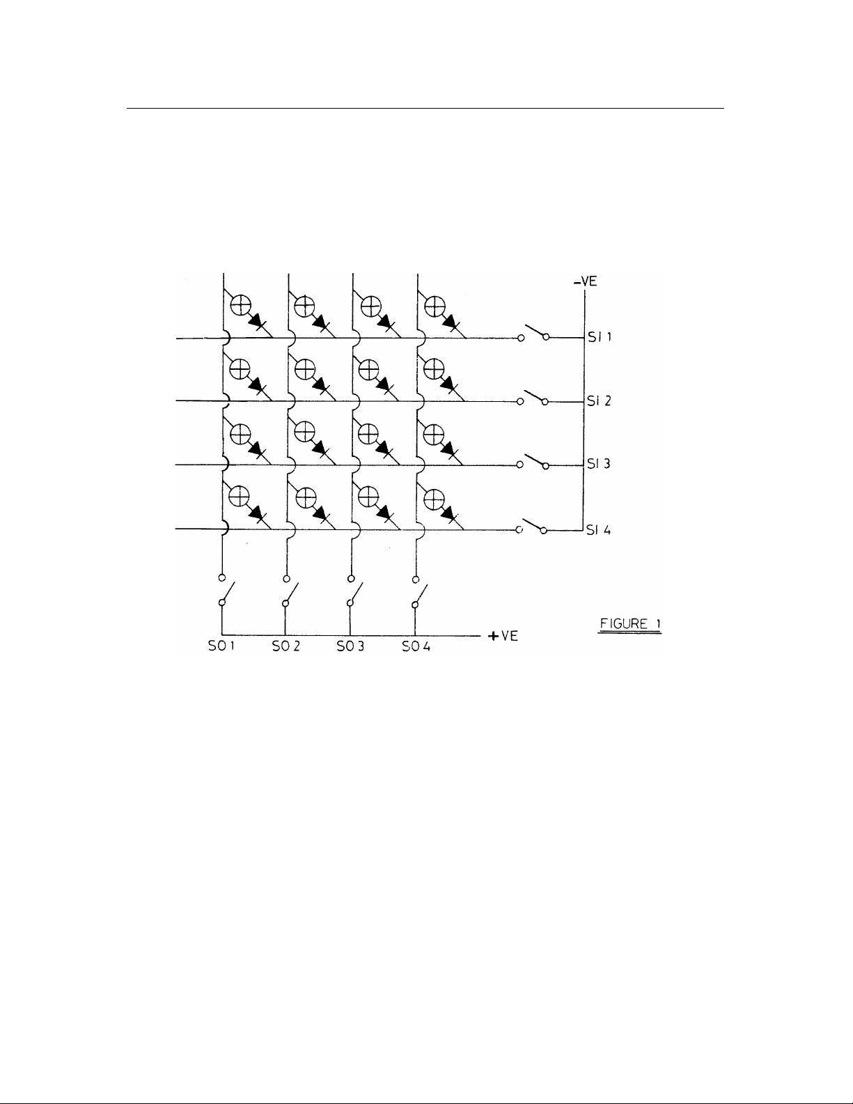
To simplify matters. Figure 1 demonstrates the principle with a 4 x 4 matrix. In this example, 16 lamps can be
controlled by only 8 transistors (shown as switches). Each lamp therefore is under control of two specific
switches. Diodes are also fitted to prevent backfeeds.
By turning on a column (So1 -So4) and by setting up data on a row (Si1 -Si4), up to 4 lamps may be turned on.
After a period of say 1 msec, the column address set up on So1 -So4 is incremented and the data on Si1 -Si4 is
changed, a second row of 4 lamps may be displayed. By incrementing the column address at a rate greater than
70Hz the lamps will appear to be continuously lit with little suggestion of flickering. Since the lamps are 12v
devices and are being switched in a 1/16 duty cycle, the supply voltage is raised to 50v DC to overcome the
reduction in effective brightness.
As long as the computer is running the 50v will be shared between the lamps as is explained above. However,
should the computer cease to run then it is theoretically possible for the lamps to burn very brightly, however a
safeguard is built in, whereby should the computer fail, then the lamps will extinguish.
Page 12

9
MULTIPLEXING -TECHNICAL DESCRIPTION
The control of the multiplexing transistors is performed by an 8255 peripheral interface element (IC 25). The
CF70000 communicates with the main processor (IC 13) via an eight bit parallel bus BD0 to BD7 pins 27 to 34
respectively. The device is memory mapped and is enabled by Sel 3.
On reset the device is disabled since I/O enable (IC25 pin 35), is high. This sets the device into the input mode
and all outputs are pulled down internally to logic zero. This disables the column transistors and therefore all
lamps are extinguished.
During operation the data for the lamp/display system is set on ports A0-A7 and B0-B7. The specific row (one
of sixteen) is set up as a four bit code on port CO-C3. A 74HC4514 is used as a four to sixteen line decoder, to
produce a specific row select. By using this method it is impossible to set up more than one row at any one time.
Because in a fault condition, it would be possible to stop incrementing the row code, and hence leave a row
permanently on and hence developing 50 volts across a 12v lamp, a counter within ULA2 is used to disable the
drives if the row code stops incrementing.
In this instance the counter input (IC 11 pin 9) will be reset by the least significant row address C0 and will
consequently timeout. This will set the output (IC 11 pin 1) to the high state which will set all outputs trom the
74HC4514 low. This in turn will set all the row transistors off and disable all outputs.
A multiplex timeout will be indicated by the bottom right hand segment of LED 5 (7 segment) extinguishing.
The outputs trom the 74HC4514 CMOS decoder are interfaced to octal transistor drives (IC34 and IC36),
whose outputs are used to drive the sixteen NPN row transistors TIPL 790's (Q17 to Q32). These transistors are
capable of sinking 8A at a 1/16 duty cycle and an ambient temperature of +60°C which allows a complete row
to be on permanently.
The maximum mean current through a row transistor is as follows:
Assuming a lamp is 1.2w then at 12v the resistance is 120R. Thus at 50v the current will be 400mA. For a
complete row illuminated therefore this current will be 6.5A. To prevent excessive heat being generated in the
transistors the devices chosen have a very low saturation voltage, typically 1.5v maximum.
The column data set up on ports A0-A7 and B0-B7 are connected to octal transistor drives (IC17 IC18) which
drive sixteen PNP column transistors (Q1 - Q16) TIP 126. A 2R ½ w resistor is used in the emitter, tor the
following reason. Firstly, on switch on of a cold lamp, the current flowing would be very high since the lamp
would inhibit almost no resistance.
The 2R2 resistor effectively limits the current to 30A. This current is still excessive, however due to the flow of
this current through the resistor, the emitter would drop below that of the base and hence the transistor will tend
to turn off, and limit the current in itself. As the lamp warms up, the current will reduce, the drop across the
resistor will reduce and the transistor will tend to turn back on. Thus the 2R2 resistors (R1 - R16) provide a
"Cold Start" for the multiplexing system, preventing transistor breakdown.
Page 13
10
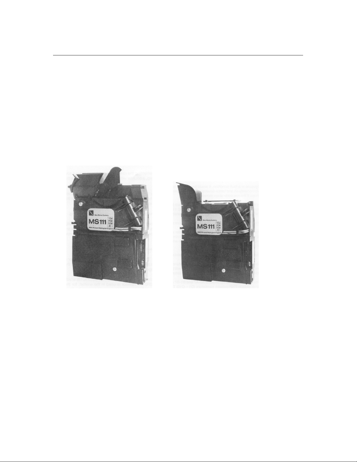
MARS 111 MULTI COIN ACCEPTOR
TOP ENTRY AND SIDE ENTRY
Operation
The coin enters the mechanism and drops on to a ceramic snubber in order to stop the coin bouncing. It then
rolls past 3 sensor coils, which measures thickness, material and diameter. If the measured values fall between
the limits in the prom, the coin is accepted via the accept solenoid opening. If one or more values are out of
tolerance the gate will not open and the coin is rejected.
Pin Connections
13 + V Common. 9 20p Output. 5 + 12v DG Supply.
12 ₤1 Output. 8 Polarising. 4 0v.
11 Polarising Key. 7 10p Output. 3 20p Inhibit.
10 20p Output. 6 10p Inhibit. 2 20p Inhibit.
1 ₤1 Inhibit.
Inhibit Inputs
Inhibit inputs are used to detemine which coins are accepted by the mechanism. Coins are accepted if the inhibits
are pulled low. If the line is pulled up or open circuit then coins will be rejected.
Inhibit Accept Level -0.5v or less,
Inhibit Reject Level -More than 2v or open circuit.
Service Instructions
Adjustments
The unit is factory programmed and no adjustments can be made in the field.
Field Test Box
It is recommended that the MS111 Field Test Box be used if it is unclear whether the fault lies in the coin
acceptor or the machine. Test boxes can be purchased directIy from Mars Money Systems at a price of
approximately ₤35.00.
Cleaning Instructions
Obviously, the mechanism will require cleaning from time to time, and it is advised that either a damp cloth or
an aerosol foam cleaner such as Ambersil Amberclens be used. To do this, unclip the mechanism from the front
plate by squeezing the two clips together and pulling the body free. The lid is spring loaded to enable coins to be
rejected, and can be opened wide for cleaning. The reject cover is retained by a single screw and can easily be
removed for further cleaning. The separator should also be cleaned.
Page 14
11
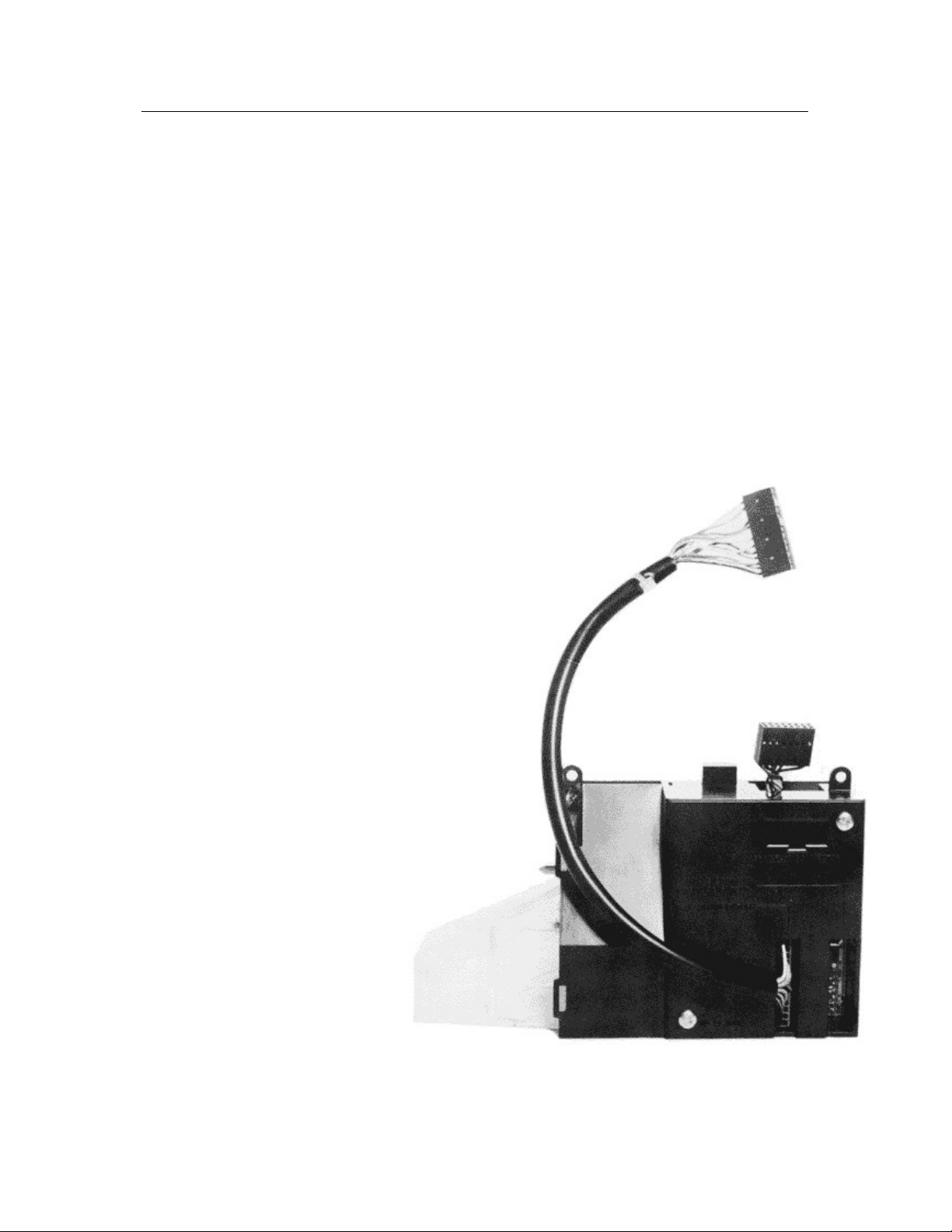
MS126 SEPARATOR
This separator is attached via two self tapping screws to the MS111 and is interconnected electrically.
The MS126 is a fully active 4 way separator unit. Two solenoids can be operated which in turn operate three
routing paddles.
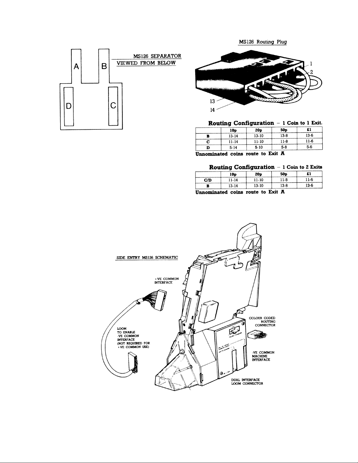
In order to enable the -VE common output, a loom is connected between the MS111 and connector 4 of the
separator.
Coin Routing
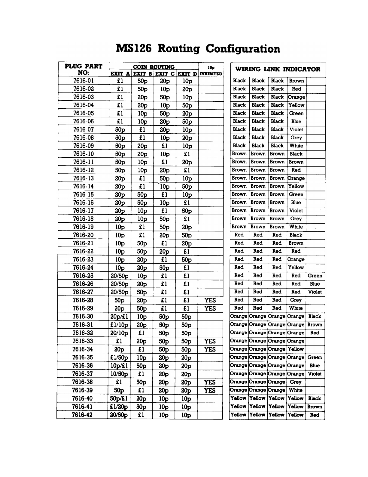
The MS126 has four coin exits from the separator unit. The routing of coins to different exits is programmed by
an MS126 routing plug. The routing plug is a 14 way polarised connector which is inserted into the separator.
The wire links within the routing plug complete the electrical circuit between the MS111 and the solenoid drive
circuitry. See MS126 Routing Configuration tor further intormation.
CONNECTOR 3: 1 - Coin output common (-12V). 8 -Inhibit 1Op.
2 - Coin output £1.00. 9- Logic & solenoid supply + 12V .
3 - Polarising. 10 -Common OV.
4 - Coin output 50p. 11 -Inhibit 20p.
5 - Coin output 20p. 12 -Inhibit 50p.
6 - Polarising. 13 -Inhibit £1.00.
7 - Coin output 10p.
Supply Voltage
+12V DC +/- 10%.
Quiescent current 25mA maximum.
Current during coin flight 55mA maximum.
Current During Solenoid Operation
Diverted coins: 2.25A maximum for 0.58 seconds maximum.
Non-diverted coins: 0.75A for 0.25 seconds maximum.
Negative common supply +0V to -13.5V maximum.
Page 15
12
Page 16
13
Page 17
14
Page 18

15
MAIN BOARD -TECHNICAL DESCRIPTION
Memory Addressing
Memory addressing is used to enable the program ROM, data RAM and peripheral devices used for switch
interfacing and output driving. AII select lines tor the above devices are generated trom two Universal Logic
Arrays (ULA's).
Two discrete EPROMS's can be addressed within MPS2, their select lines being ROMSEL 1 and ROMSEL 2,
IC11 pins 20 and 21 respectively. These lines go off board to the memory card. The type of EPROM fitted, and
hence the required addressing range of ROMSEL 1 and ROMSEL 2, is set by two links on the memory board.
These links interface into the ULA as S0 and S1. These two lines allow the system to be configured for the use
of 64K (2764), 128K (27128) or 256K (27256) EPROMS.
The on-board RAM, IC23 is selected via the control lines RAM CS 1 and RAM CS 2 IC11 pins 27 and 33
respectively. This is a 2K x 8 CMOS device and is the main non-volatile store. The selection of the RAM is
controlled by both ULA 1 and ULA 2, these protect the data within the RAM against corruption in the case of
power failure. As an added safeguard IC35 (PCF 1251P) keeps the RAM disabled during power up or down.
The reset to the RAM is generated from a precision voltage reference and a comparitor, D22 and one half of
IC31. This monitors the level of the +5v line and goes low if the +5v drops below +4.5v. Thus the RAM will be
disabled before any malfunction might occur due to a low supply line. The reset system will be dealt with in
more detail in the section dealing with interrupts.
Four further memory mapped enable lines are generated by ULA 2. These are SEL 0, SEL 1, SEL 2 and SEL 3,
pins 37,36,35,34 and 4 respectively. These lines enable the peripheral interface elements, whose specific
functions will be dealt with in their relevant sections (multiplexing, input interfacing and output interfacing).
To allow tor the interfacing of slow peripheral into the system, circuitry within ULA 2 can generate a wait state
i.e. extension of the memory access time by one clock period. Selection of wait states tor the peripherals is
enabled by link 2, WAlT EN. With link 2 in wait states are disabled.
Link 1 is used to disable or enable the ready circuitry. If this link is removed, all memory cycles will have wait
states inserted. When the link is inserted only peripheral addressing will be subject to wait states. Both links are
not user selectable and are loaded at the time of board manufacture.
To allow the use of the full address range trom an external source, the ULA 2 enable lines tor I/O may be
disabled by setting I/O select disable, IC11 pin 8 to the low state. This will inhibit generation of SEL 0, SEL 1,
SEL 2 and SEL 3 allowing extra I/O to be interfaced.
The memory select lines may also be disabled by the use of a line present on the bus expansion socket.
MEMMAP EN HD5 pin 6C (see 045165 sheet 1). This line, when set low, puts S0 and S1 high which disables
the selection of ROMSEL 1, ROMSEL 2 and RAMSEL.
Page 19

16
CRU Addressing
CRU addressing is a method which allows multiple I/O bits to be interfaced on three lines (CRUIN, CRUOUT
and CRUCLK). The 9995 is capable of interfacing up to 32K bits, although only a small amount are actually
used on MPS2.
Four main units are addressed via CRU and their enable lines are generated by circuitry within ULA 1 IC15
ENO, 1, 2 and 3.
Again as in the memory mapped I/O the CRU enable lines are also disabled via the I/O select disable line, IC15
pin 8. Thus, the full CRU address range is also available from an external source and interfacing of extern al
CRU functions is very simple. The use of this line requires minimal decoding logic on the main board, since the
CRU addresses are allowed to repeat themselves. This then allows simple enable logic to be used in a stand
alone system, thus reducing the cost of the main board.
The CRU enable lines are used for the following functions:
A. ENO - Serial Link 0
ENO is used to enable one of the two on-board UART's, IC5. This UART is used as the interface to a
printer or security system.
B. ENI - Interrupt Status (Internal to the ULA) ENI is used to enable the read/write logic associated with the
interrupt latches within the system. Using a CRU read instruction, ENI allows the reading of the interrupt
status lines, whereas usually a CRU write instruction allows the resetting of an addressed interrupt latch.
The operation of this logic will be dealt with in the section covering interrupts.
C. EN2 - Serial Link 1 EN2 is used to enable the UART, which communicates with the on-board reel drive
processor. This processor will be dealt with in its relevant section.
D. EN3 - System Function Lines (Internal to the ULA) EN3 is used to write eight bits of CRU allocated to
system functions.
The functions with their uses are as follows:
(1) BB/PTR - Internal to IC15. This line is used to direct serial information from UART 0 IC6 to either
the black box (if low) or to the printer (if high).
(2) I/O Enable - IC15 pin 38. This line is used to enable the peripheral devices selected from SEL 0,
SEL 1 , SEL 2 and SEL 3. It's normal state is high, but will go low under reset conditions.
(3) Reel Drive Enable - IC15 pin 39. This line is used to enable the reel drive processor. lts normal state is
high (i.e. processor enabled).
(4) NMI EN - Internal to IC15. This line is used to disable the generation of the NMI interrupts. lts normal
state is high, but it goes low to inhibit NMI interrupts.
(5) Alarm - IC15 pin 34. This line is capacitively coupled into the amplifier system to generate an alarm
sound. An alarm is produced when this line to toggled.
(6) RAM Enable - IC15 pin 33. This line is used to enable and disable the RAM under program control. lts
normal enabled state is high.
(7) Watchdog Strobe - Internal to IC15. This line is toggled to retrigger the watchdog circuitry.
Page 20

17
Interrupt lnterface
The 9995 allows the interfacing of up to three external interrupts as well as a reset line. The interrupts are as
follows in order of priority.
A) RESET.
B) NMI.
C) INTI.
D) INT4.
Each interrupt will now be dealt with in more detail.
A) RESET - IC31 PIN 7
This signal is the main processor reset, which is produced on power on, or when the +5v line falls below
+4.5v.
The output from the device is used to reset a counter within IC15, which produces a long reset pulse of
approximately 4 seconds on IC15 pin 27.
B) NMI - IC16 PIN21
The non-maskable interrupt, NMI, is the next highest priority interrupt. This is used for major system
interrupts, where four separate interrupts are ored together to produce an NMI interrupt. These are:
(1) Mains Failure
(2) Invalid Memory Access.
(3) Watchdog timeout.
(4) On board switch (as Lev 3 in system 80).
All NMI processing is performed within IC16.
(1) Mains Failure NMI
The highest priority interrupt within the NMI interrupt is mains failure.
An AC winding from the power supply of 48v peak to peak is rectified by D23. The signal is used to
reset a counter, which has a timeout period of approximately 30 msec. If the mains is not present, the
counter will timeout and proved an interrupt source for an NMI.
(2) Invalid Memory Access NMI
The next highest NMI is the invalid memory access interrupt. If at any time the software attempts to
write to a ROM location or execute code in RAM, an invalid memory access will generate an NMI
at the processor.
(3) Watchdog Timeout NMI
The next highest NMI is the watchdog timeout interrupt. During normal execution of code, the
watchdog is strobed. This line is used to reset a counter, which has a timeout period greater than the
period used to set and reset watchdog strobe. If the software is caused to function incorrectly, and
this line is not strobed (due to static etc.) the counter will timeout, thus setting up the requirements
for an NMI.
(4) Reset Switch NMI
The last NMI interrupt source is the reset switch (Lev 3 in system 80) used for software resetting of
RAM after any RAM corruption. Closure of this switch will set up the conditions for an NMI to be
generated.
C) INTI - UART Interrupt
Interrupt 1, IC16 pin 15 is sourced via IC15 pin 29. The two inputs URT1 and URT2 are the interrupt outputs
from the two on-board UARTS, IC5 pin 1 and IC10 pin 1 respectively. A low level on either will define an
interrupt condition.
D) INT4- Meter Interrupt
On removal of the meter plug HD9, IC16 pin 14 will go low to produce an interrupt.
Page 21

18
Serial Communication
MPS2 has two two-serial communication channels. One is used exclusively for communicating with the reel
drive processor, while the other UART is used for communicating with either a printer or security unit.
A) Reel Drive Communication - UART4
A TMS 9902A, IC10, is used to communicate to the reel drive processor. The UART is controlled via the
CRU bus and is enabled via EN2, IC10 pin 17.
For communication on-board (i.e. to the reel drive processor), the receive and transmit lines are multiplexed
onto a single line, peripheral communication. For off-board communication separate RX and TX lines are
used, which conform with RS232 levels. These lines, PTX and PRX appear on HD3 pins 1 and 3
respectively. Level translation to and from RS232 levels are provided by IC2 pin 3 for the transmit mode and
IC1 pin 1 for the recieve side. IC10 pin 1 is in the interrupt output from this UART defining receive data or
transmit data.
B) Printer/Black Box Communication - UART2
The second TMS 9902A, IC5, is used for communication to and from a security unit or to a printer. This
UART is also controlled via the CRU bus and is enabled by ENO.
All lines from this UART (RX, TX, CTS, RTS and DSR) conform to the RS232 requirement and interface to
the board via HD3 for the printer or PL1 for the security unit.
Logic within ULA 1 is used to divert the transmitted data to either the black box or the printer.
IC5 pin 1 is the interrupt output from this UART. This interrupt is used to receive and transmit data.
Coin Handling, Switched Inputs and Outputs.
This part of the system is composed of four distinct areas. These are coin handling on HD10, meter outputs on
HD9, undefined direct outputs on HD8 and switch inputs on HD11.
1. Coin Handling - HD10
The coin handling interface allows tor the following:
A) Four coin inputs (open collector NPN transistors).
B) One coin input (Microswitch).
C) Four non-payout sensors.
D) Four level detectors.
E) Four TTL inhibit outputs.
F) One high current NPN output (series 10 inhibit).
G) Four high current NPN outputs (DC solenoid drives).
AII input and output lines are interfaced into the system by two 8255 peripheral devices, IC21 and IC26.
IC21 is used tor all outputs and IC26 is used for all inputs.
The coin inputs are interfaced into the system on inputs 19 to 23 in the same manner as system 80 (a 1K and
2K2 resistive divider chain pulled down to -12v). In normal operation all devices operate as current sinks to 12v and input 19 is contigured to allow this by adding LK12 only. Inputs 20 to 23 are used for current sinks
with LK6-9 not loaded, whereas for current sources inputs 20A - 23A are used with LK6-9 loaded.
Low level inputs are interfaced into input 24 to input 27 and non payout detectors are interfaced into input 28
to input 31.
The Coin inhibit lines and payout drives are all generated by IC26. Port A - A0 to A2 and port B - B7 are
used to drive tour transistors Q34 to Q37, ZTX 450, used for payout drives, and Port B - B0 is used to drive
Q33, ZTX 450, used to drive the lockout coil of a series 10 mechanism. An LS541 buffer, IC28, is used to
provide sufficient drive to the transistors and is disabled by Port A - A3. This ensures that on power up, when
all outputs from the 8255 device are contigured as inputs, no spurious payouts occur. Since IC28 pin 19 will
be high, all outputs trom IC28 will be tristate and, due to Sil 10, the base of each transistor will be pulled
down, turning the transistors off .When paying out, port A - A3 is set low, which enables the LS541 and
allows it to turn on the transistors.
Inhibit lines output 7 to output 10, for a multi-mechanism are driven from Port A - A4 to A7 and are
interfaced to the mechanism by a 7407 open collector driver .
Page 22

19
2. Meter Outputs -HD9
HD9 is capable of driving up to nine meters, output 15 to output 23. Port C -C0 to C7 of IC26 is used to
generate eight meter drives, output 16 to output 23. Port C drives an Octal darlington array IC23 to give the
required current drive. Output 15, for the ninth meter, will be covered in section 5, since this is driven from a
separate 8255 device.
Detection of the removal of the meter plug is achieved by IC27.lf the plug is removed INT4 is asserted and
generates a system interrupt.
3. Undefined Direct Outputs -HD8
Six open collector outputs are interfaced into HD8. These are generated by IC26 port 8 - B1 to B6, which
drive an octal darlington array IC33.
4. Switch Inputs -HD11
Switch inputs are interfaced into the system via IC21. Operation of the 8255 peripheral devices is covered in
section 1, detailing the generation of SEL 0 and SEL 1, and section 2, detailing the internal register operation.
Complex Sound and Switched Inputs
The final eight switch inputs, input 11 to input 18, are interfaced into IC22 Port A -A0 to A7. The ninth meter
drive is generated on port C - C3, which drives IC33 on sheet 4.
IC22, Port B - B0 to B7, is used to interface an 8 way dil switch into the system, SW3. A hex rotary switch, SW1
is interfaced into the system on port C - C4 to C7.
The complex sound generator, IC6 -SN76489, is also interfaced on Port B - B0 to B7 and controlled by Port C C2. Data is set up on Port B and latched into the sound chip by setting and resetting port C - C2. Since the device
is a slow peripheral and requires 32 clock cycles to complete an operation, logic within ULA2, is used to keep
the chip enabled, thus Port C - C2 may be removed early, without affecting the timing of the sound chip, and
thus not putting software overheads on the main processor .
The sound output, IC6 pin 7, is amplified by an on-board amplifier, IC3 - LM380, whose volume is controlled by
VR1.An alarm input is also interfaced in to the amplifier, via R29 and C15, which is not controlled by VR1 and
therefore is always enabled independent of the volume setting. The speaker outputs are interfaced into DH3 pins
8 and 9.
Page 23

20
Reel Drive Circuitry
Control of four 1.8 degree stepper motors is accomplished by the use of a pre-programmed single chip processor
TMS7041 IC14. More detailed information on this device may be found by consuiting the TMS7041 Data
Manual from Texas Instruments.
Internally the 7041 consists of an eight bit processor, with 4K bytes of ROM and 128 bytes of RAM. Externally
in this application, the device consists of one serial channel, used for communication to the main processor,
sixteen output ports, used to drive the motor phases, and six input lines, used to interface the four reel optos and
two peripheral address lines.
The four reel optos are interfaced via port A- A0 to A3, pins 6 to 9, and are TTL compatible. Since the 7041
communicates on a single serial channel, the device is programmed to recognise a specific address code
identifying it as being addressed. This code is set up on Port A - A4 and A7, IC14 pin 10 and 11, which allows
for up to four peripherals to be interfaced on to the serial bus.
The phase outputs are generated on Ports C and D - C0 to C7, and D0 to D7 of IC14. These outputs drive two
octal darlington arrays IC7 and IC8 whose collectors are connected to the motor phases. Diodes D1 to D16
IN4148, prevent the collectors of the transistors from going negative, whereas D17 and D18 ensure the collectors
are clamped to 48v maximum.
Unlike system 80, the collectors are allowed to rise above the reel voltage (Vreel) by an amount defined by the
zener diodes D17 and D18. This ensures that there is sufficient energy in the system to allow the reels to run at
typically 100 r.p.m. A value of 24v for the two zeners is sufficiently high enough to ensure that most of the
available energy is transmitted to the phase windings, but is low enough to limit the maximum allowed collector
voltage.
Since the 7041 has an on board oscillator, the only components required to generate the system clock are a 5Mhz
crystal XTAL2 and two 27pf capacitors C28 and C29.
All connections to and from the reel drive circuitry are via a 50 way double row header HD2. Pins 14, 15, 34 and
35 are the sources for the reel optos (via 180R resistors R21 to 23) and pins 39, 30, 10 and 19 are the inputs from
the reel optos, which are read via A - A0 to A3, pins 6 to 9 of IC14.
Pins 1, 2 and 4 are three sink lines paralleled from the multiplex circuitry and pin 47, 48,49 and 50 are four
source lines from the same circuitry. These are used when reel illumination is required and allows for up to three
lamps on four reels. Pin 41, reel int, is used to detect the removal of the reel plug, or when using a modular reel
mechanism, the removal of a single reel station. When this link is broken, IC15 pin 19 will go high, which due to
the inversion of the ULA1 , will generate a low level on the interrupt input to the 7041, IC14 pin 13. Detection of
this occurence will generate a code to be communicated to the main processor via the serial link, where
appropriate action may take place (e.g. alarm generation, freeling of game, etc.).
Page 24
21
Page 25
22
Page 26
23
Page 27
24
Page 28
25
Page 29
26
Page 30
27
Page 31
28
Page 32

29
LINEAR POWER SUPPLY TECHNICAL DESCRIPTION
1) Single Pole Mains Fuse
This fuse is found on the left hand side of the front panel. The fuse is held in a bayonet type fuse holder
which unscrews to give you 1 ¼ " x ¼ " 2A quickblow.
2) Filter
The filter IFCHI has two basic functions, these are:A) To attenuate any transient voltages present on the incoming mains supply.
B) To stop any conducted radio interference which may be generated within the power supply itself.
3) Double Pole On-Off Switch
The rocker switch which can be found on the left hand corner of the front panel.
4) Voltage selector
The voltage selector comprises of a single pole 3 way socket mounted onto the front panel. The voltages can
be selected by inserting the plug into the appropriate voltage position i.e. 200v, 220v or 240v.
5) Mains Transformer
The mains transformer is of the double wound isolating type with tapped primary accessible via the voltage
selector. The transformer has 4 isolated secondary windings for the unregulated and AC outputs. There is also
a center tapped, push secondary coil to feed the linear regulated circuits. The screen and core is securely
fitled to the main chassis using screws and spire clips.
6) Rectifiers
The rectifiers Rec 1 and Rec 2 are to provide unregulated voltage for both the reel and lamp circuitry. Both
rectifiers have a set of smoothing capacitors C9 and C14, and discharge resistors R20 and R21.
7) smoothing Capacitors
There are two large reservoir capacitors in the power supply, which smooth the unregulated voltage for the 5v
and 12v regulated supply.
8) Front Panel Assembly
A. Fuse Panel
Accessible via removeable front panel. Shown below are the fuse allocations and recterys.
FUSENO CIRCUIT FUSE RATINGS
F1 Monitor (when fitled) 2A
F2 Hopper 3A
F3 Synch 0.25A
F4 Triac 5A
F5 Lamp 5A
F6 Reel 2A
F7 Crowbar 2A
Note -all fuses cartridges are 1 ¼ " x ¼ " glass quick blow.
N.B. -isolate mains before removing front fuse cover.
B. Output Connections
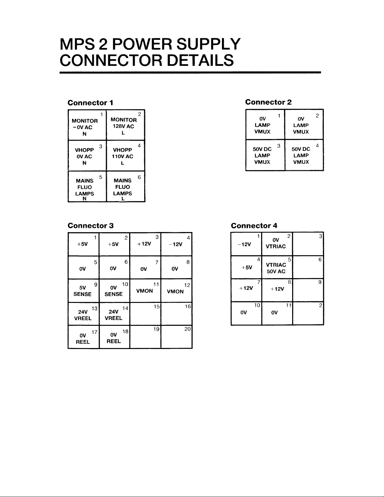
The output connections are visible on the front panel and are marked from Con 1 to Con 4.
C. Reel Supply
The reel drive supply voltage is made up of Rec 1 D5- D8, i.e. 4x 1N 5402. The smoothing capacitor C9
2200 mf and the discharge resistor R20, 10K.
Page 33

30
D. +5v Supply
The components that supply the +5v are as follows: D1 - D4 i.e. 4x 1N 5402, TR2 TIP 3055, (TR3 when
fitted, TIP 3655) ICI, MC 1723, VR2, 1K 0.5W, R2 100R, R4 100R, R5 100R, R11 1K81%, R12 2K2,
R13 2K2, R15 6K8, R24 1R, R26 5K6 C13 100n. (C9 remote 2,200mF 16v).
The +5v supply consists of basically a push pull type rectifier, a remote smoothing capacitor C13
22000mf 16v, a series pass transistor, TR1 and a current source resistor.
The overall closed loop voltage and current control is achieved using a MC 1723 IC2. which is a variable
voltage regulator .
The supplies output characteristic is a constant voltage curve up to 115% set load current, folding back to
50% under short circuit conditions.
E. +5v Under Voltage Circuit
There is an under voltage circuit built into the 5v supply whose components are IC3 LM311P ZD2 5V6
ZD3 5V6 VR3 1K C6 - C7 47MF 25V, R6 220R, R7 - R9 1K, R18 - R19 47K, R25 1M 5%.
The under voltage circuit uses an LM 311 (IC3) which is a fast comparitor which monitors the 5 volt
unregulated supply. If the 5v unregulated supply falls below a certain limit the LM 311 (C3) will inhibit
the MC 1723 (IC1), which is a voltage regulator before the +5 volt falls below bottom limit. The +5v
under voltage circuitry is self resetting.
F. +5v Over Voltage
As the 5v supplies the voltage for the logic circuitry on the main MPS 2 board, it is imperative that the 5v
stays within very accurate tolerances, which is why there is need tor a 5v under and over voltage circuitry.
The +5v overvoltage circuitry consists of TH1 C106Y1 , ZD1 6V2 R147R C5100 mf 10v and the crowbar
fuse cartridge F7 2A.
The over voltage circuit functions as a single shot crowbar circuit i.e. if the output ot the 5v line exceeds
6.2v, the 6v2 zener diode ZD1 will conduct so causing the thyrister C106Y1 TH1 to be activated, which
will then either put the regulator into current limit or blow a fuse in the 5v Iline F7 2A.
G. + 12v Supply
The components used to create the + 12v supply in the power supply are as follows:
D9 INS 5402 D10 - D12 IN 5402, IC2 MC1723, TR1 TIP 3055, R3 100R 5%, R16 6K8, R17 4K7 R23
25R, VR1 1K 20%, C12 100m 35v and C10 remote 1000mf 25v.
The + 12v supply is made up a push pull type rectifier, a remote smoothing capacitor C14, a series pass
transister TR2 TIP 3055 and a current series resistor. The overall closed loop voltage and current control
is achieved using a MC 1723 (IC2), which is a variable voltage regulator.
The only difference between the generation ot the 5v supply and the 12v supply is that the 12v supply has
a constant current and constant voltage characteristic.
H. -12v Supply
The components which make up the -12v supply are as follows D13 - D14 1N4002 IC4 LM 7912 C8 47uf
C11 470 mf 25v R10 1K.
The -12v supply comprises of a push pull type rectifier, smoothing capacitor C11 470mf 25v and a MC
7912 CT which is a monolithic voltage regulator, which is placed under resistive capacitive load.
Page 34
31
Page 35
32
Page 36
33
Page 37

34
PARTS LIST FOR LINEAR PCB
QTY DESCRIPTION LEGEND REF
1 25WCARH/STAB47R5% R2
4 25WCARH/STAB100R5% R2-R3-R4-R5
1 25W CAR H/ST AB 220R 5% R6
4 25WCARH/STAB1K5% R7-R8-R9-R10
2 25WCARH/STAB2K25% R13-R14
1 25WCARH/STAB4K75% R17
1 25WCARH/STAB5K65% R26
1 25WCARH/STAB6K85% R16
2 25WCARH/STAB475% R18-R19
1 25W CAR H/STAB 1 M 5% R25
1 5W CAR H/STAB 1 OOR 5% R22
2 5WCARH/STAB10K5% R20-R21
1 25WM/FILM1K81% R11
1 25W M/FILM 2K2 1% R12
1 25W M/FILM 6K81 % R15
1 7WW/W 1R 10% R24
1 4W W/W R251 0% R23
3 0.15WH/PRE1K20% VR1-VR2-VR3
3 47uF25VR/CAP C6-C7-C8
1 100uF10VR/CAP C5
1 1000uF16VAX/CAP C10
1 270uF 25V AX/CAP C11
1 2200uF 35V AX/CAP C9
1 10,000uF25V AX/CAP C14
2 100n 30V D/CER CAP C12/C13
2 4700pFRIFACAPY C2-C3
1 22uF 250V CAP X C1
1 33n RIFACAPX C4
1 VARISTERV275LA44 MOV1
1 MZX 79C6V2 DIODE XD1
2 BZX 79C5V6 DIODE XD1 - ZD3
2 1N4002DIODE D13-D14
12 1N 5402 DIODE D1 to D121NC
1 C106Y1 THYRISTOR TM1
2 TIP3055TRANSISTOR TR1 -TR2
1 LM7912CTV/REG IC4
2 MC1723CPV/REG IC1-IC2
1 LM311PV/COMP IC3
1 I/PFILTERCHOKE IFCH1
1 MRIICON4WAY CON2
1 MRIICON6WAY CON1
1 MRIICON12WAY CON4
1 MRIICON20WAY CON3
14 FUSECLIPS
6 LlNKSMALL LK1-6
2 LINKLARGE LK7-8
Page 38
35
Page 39
36
Page 40
37
Page 41
38
Page 42
39
Page 43
40
Page 44

41
TECHNICAL DESCRIPTION
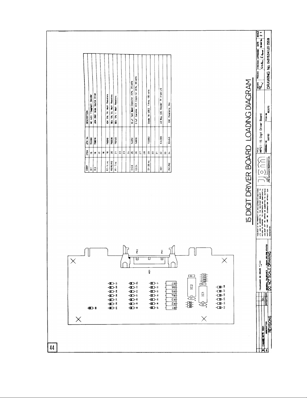
15 Digit Driver Board
This board is capable of driving up to 15 seven segment displays, all displays are bussed with their common
cathode connections switched by the sink transistors trom the MP8 1 multiplexer array, thereby torming a
separate display matrix.
The board carries the sink & source connections as weil as the control ~ircuitry tor the 15 digit display. The
source 8010-8015, sink 810-815 connections are brought onto the board via edge connectors A & B respectively,
then transferred to the display board via diodes 08-028 & lOC connector H01.
Sink lines 810-8114 are used to strobe the digits on the display board. As each digit is strobed, the corresponding
BCO data is output via tour direct outputs OP2-0P5 & presented to the board edge connector A. This information
is decoded by IC1 (MC 14511) a BCO to 7 segment decoder chip. The output of the MC 14511 is transmitted to
the segments of the L.E.O.'s via IC2 (UON 2981 A) a high current source driver chip and 7 x 68R 1 watt current
limiting resistors.
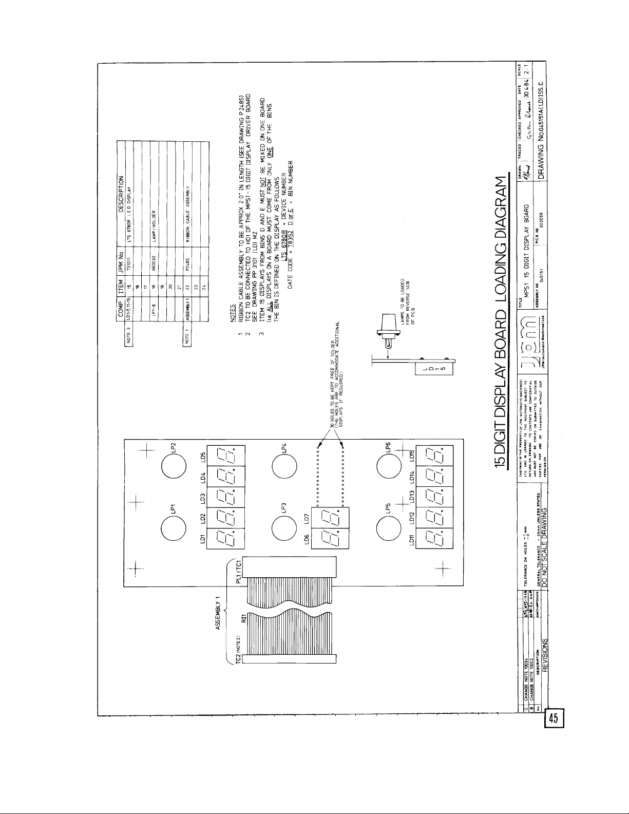
15 Digit Display Board
This board can be loaded with up to 15 seven segment displays (L T8 6780R) in three groups of 5, it also has
provision tor the insertion of up to six 12v 1 w lamps. Each 12v lamp is held in a twist 'n' lock holder fitted into
holes in the PCB.
All drive circuitry tor this board is contained on the 15 digit driver board (045152) and all interconnections are
made using a 40 way ribbon cable assembly 080053 terminated onto the board at H01.
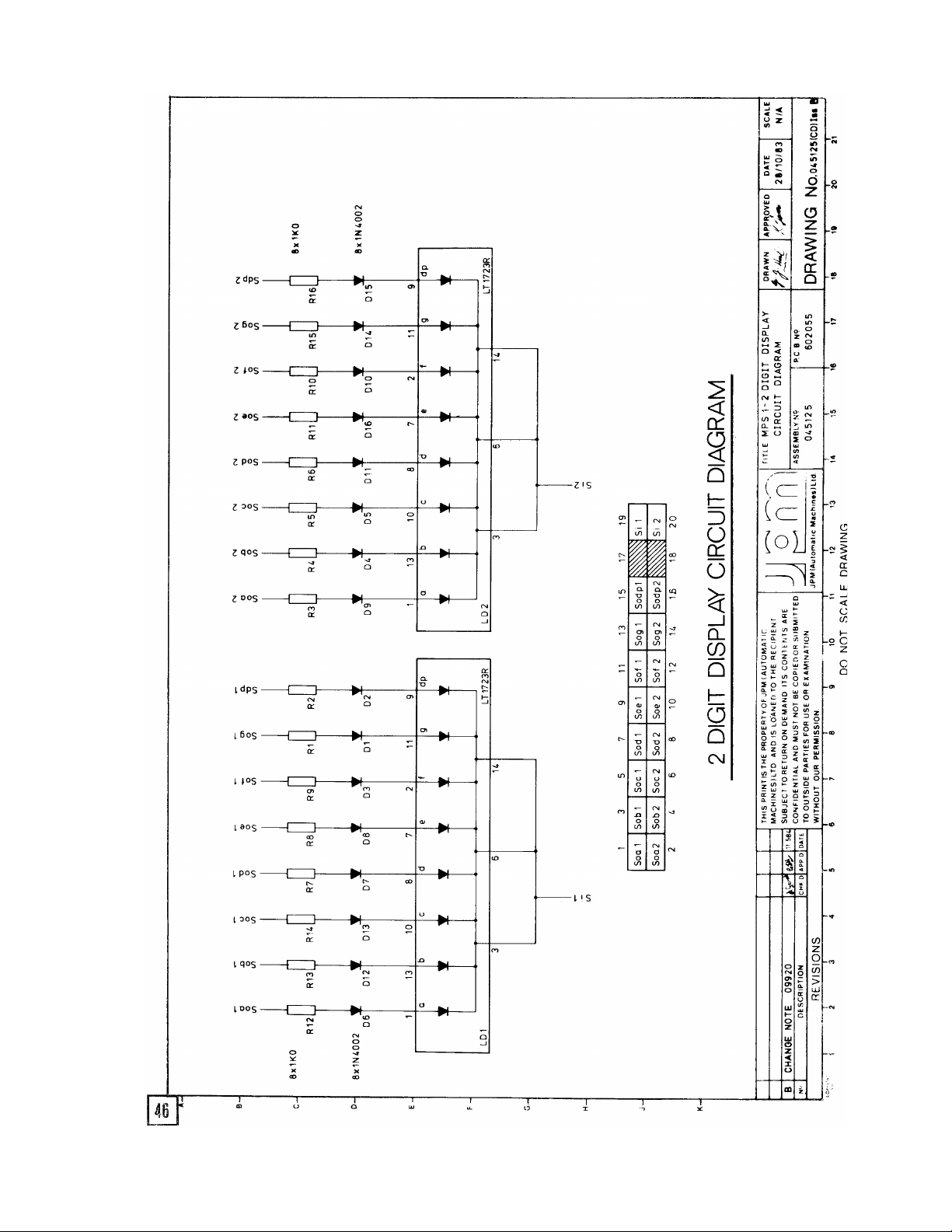
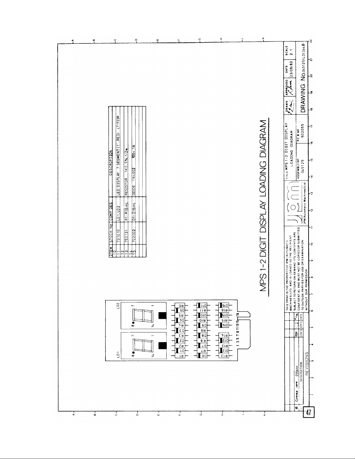
2 Digit Display Board
This board is loaded with two 7 segment displays (L T 1723R). The board is connected to a push in 20 way edge
connector and is driven by multiplexing of the MP81 and MP82 main boards.
8 Digit Display Driver Board
This board can drive up to tour 1 " 2 digit display pcb's. The board contains a 40 way header W1 which is fed
direct I y trom the multiplexing circuitry on the MP81 or MP82 main boards. There are also tour 12 way headers
W2 -W5, each header driving one 2 digit display. This board also contains additional multiplexing components
R1 -R16 and 01- 020.
1"-2 Digit Display Boards
Each board comprises of 2 x L T81723R seven segment common cathode displays and one 10 way header W1.
The displays are driven direct I y trom the 8 digit display driver pc b via W1 .
Page 45
42
Page 46
43
Page 47
44
Page 48
45
Page 49
46
Page 50
47
Page 51
48
Page 52
49
Page 53
50
Page 54
51
Page 55
52
Page 56
53
Page 57

54
 Loading...