

Page 1

V333DA
AMD Socket A Athlon/Duron
使 用 手 冊
處理器主機板
編號:
發佈日期:2002 年 3 月
G03-V333DAR1C
商標:
∗ Athlon 和 Duron 都是 AMD 公司的註冊商標。其他商標及名稱皆屬其所屬公司所有。
∗ 包含在此文件之規格及資料僅為使用資訊的提供,任何修改將不另行通知,並且不應
視為廠商的承諾。
Page 2

使用者需知
手冊版本資訊
散熱解決方案
第一章
V333DA
主機板特性
1-1
規格
1-2
性能表
1-3
設計圖及跳線設定
1-4
第二章 硬體安裝
硬體安裝步驟
2-1
檢查主機板的跳線設置
2-2
安裝
2-3
2-3-1
2-3-2
安裝記憶體
2-4
擴充卡
2-5
2-5-1
2-5-2
2-5-3
2-5-4 AGP
連接埠,接頭
2-6
2-6-1
2-6-2
啟動你的電腦
2-7
目 錄
......................................................................................1
..................................................................................2
..................................................................................2
主機板簡介
.....................................................................................................3
................................................................................................................. 4
............................................................................................................. 5
.........................................................................................6
.................................................................................................8
CPU .........................................................................................................10
常用術語
關於
............................................................................................................. 13
擴充卡安裝程序
為擴充卡指定
主機板的中斷列表
連接埠
接頭
........................................................................................................10
AMD Athlon 及Duron 462-
.....................................................................................................12
IRQ .........................................................................................
插槽
.......................................................................................................
.................................................................................................15
...........................................................................................................
...............................................................................................................17
.................................................................................................20
.................................................................................8
腳座
CPU .............................................
............................................................................................13
........................................................................................
11
13
14
14
15
第三章
3-1
3-2
3-3
3-4 CMOS
3-5 BIOS
3-6
3-6-1 DRAM
3-6-2 AGP
3-6-3 PCI
3-7
3-7-1
3-7-2
3-7-3
BIOS
進入
SETUP ...................................................................................................21
線上說明
主目錄
晶片組參數的進階設定
周邊配備設定
............................................................................................................. 22
的標準設定
特性的進階設定
內建之
內建裝置之功能設定
內建超級
介紹
.........................................................................................................22
........................................................................................23
.................................................................................. 25
.................................................................................27
的進階控制
時脈設定
時脈設定
.................................................................................................29
裝置的功能設定
IDE
之功能設定
IO
.............................................................................28
....................................................................................28
..................................................................................... 29
................................................................30
............................................................................31
.....................................................................31
i
Page 3

電源管理的設定
3-8
3-8-1
3-8-1.1 IRQ
3-9 PNP/PCI
3-9-1
系統環境狀態監控之設定
3-10
其它控制設定
3-11
載入原廠預設值/最佳化之設定
3-12
設定監督者/使用者密碼
3-13
省電管理之喚醒事件的設定
組態設定
IRQ
.............................................................................................33
................................................................34
的工作範圍
..........................................................................35
........................................................................................ 35
的共用資源
.................................................................................36
...........................................................................36
................................................................................................37
.................................................................. 38
.............................................................................. 38
第四章 驅動程式及附贈軟體的安裝
支援
WINDOWS 95/98/98SE/ME/NT4.0/2000 的MAGIC INSTALL
4-1 VIA 4 IN 1
4-2 SOUND
4-3 PC-HEALTH
4-3-1
如何
4-4 MAGIC BIOS
4-5 PC-CILLIN
如何關閉內建式音效卡
4-6
怎樣更新
4-7
BIOS .............................................................................................47
安裝
VIA
安裝
使用硬體監控程式
AC97
安裝
WINBOND HARDW ARE DOCTOR
安裝
BIOS
安裝
PC-CILLN2000
........................39
四合一驅動程式
音效驅動程式和
....................................................................43
線上升級公用程式
.................................................................................47
....................................................40
EDITING/PLAYBACK
.............................................44
防病毒程式
......................................45
硬體監控程式
軟體
.......42
......43
ii
Page 4

使用者需知
本手冊的版權屬於其製造廠商。其中的任何部分(包括所描述之產品和軟體)都不允
許在未經其製造廠商書面授權的情況下以任何形式或者採取任何方法複製、傳播或翻
譯成任何語言。
本手冊包含了使用
足使用者的需求,如有任何改變或修正將不另行通知。廠商提供本手冊是不帶任何方
式的擔保,而且將不對一切直接的、間接的、特殊的、偶然的或是因此而產生的損害
(包括利潤損失,商業損失,使用數據時的損失,商業中斷等等)負責。
本手冊所使用的產品名稱及公司名稱可能不是其註冊商標或其註冊版權。僅用於說明
或解釋之作用,並無意侵犯其所有者的權益。
V333DA
主機板所必須的所有資訊,並且我們確保本手冊能完全滿
1
Page 5

手冊版本資訊
版本 版本記錄 日期
1.0 第一版 2002 年 3 月
Item Checklist
5 V333DA
5 IDE/Floppy
主機板應用程式光碟片
5
□
USB Port 3/4
5 V333DA
AMD Athlon™/Duron™
主機板
使用手冊
排線
排線 (選配
)
中央處理器的散熱解決方案
–
風扇
由於科技的日新月異,中央處理器 (CPU) 亦持續往更快速、更高的效能發展。因此在
建置電腦系統時,散熱的處理變得越來越重要了,一個適當的散熱環境,是讓系統更
加穩定及長期操作時的關鍵。提供適當散熱環境的最終目的,則在於維持中央處理器
之溫度,能低於電腦機殼之最大特定溫度。
一個好的風扇,除了要有較高的轉速外,適當的散熱片面積亦是相當重要的因素。它
可透過其表面之散熱片區域的範圍,集中來自中央處理器的高熱,並透過附加的風扇
讓熱氣流傳導出去。除此之外,散熱膏亦能有效的將高熱由中央處理器傳輸到散熱
片。為了達到散熱傳導的最佳效果,AMD 建議您使用散熱膏,並以固定夾將風扇附加
在處理器上。
當您為系統選擇適當的風扇時,請參考以下網址中 AMD 所推薦與 AMD 處理器一起使
用之風扇。
有關 AMD Athlon / Duron 處理器之散熱片及風扇銷售廠商,請至以下網址:
http://www1.amd.com/products/duron/thermals
http://www1.amd.com/products/athlon/thermals
2
Page 6

第一章
V333DA 主機板簡介
1-1 主機板特性
V333DA
可支援
用
200MHz/266MHz (Double Data Rate
Socket-A
是針對
AMD
封裝設計,且記憶體可擴充至
新一代
Athlon/Duron/
Athlon XP
,
3.0GB
。
處理器所設計,
雙倍資料傳輸率技術
其前端匯流排
的頻率。它
)
採
此主機板採用最新的
Data Rate)
DDR DRAM
的硬碟,全面提高系統性能。
記憶體介面提供了一條通往
的升級途徑。同時,它還提供了
VIA KT333
晶片組,
266MHz
其
133MHz/266MHz/333MHz (Double
處理器和
ULTRA ATA 133
DDR200/DDR266 /DDR333
介面以支援
ATA-133
V333DA
給你帶來最佳音效品質及相容性。另外,對那些需要更強大圖像性能的使用者,該主
機板則提供有
還具有內建式整合型
AGP 4X
模式的插槽供使用者使用。
AC’97 2.1 CODEC
,能與
Sound Blaster Pro
完全相容,
另外,這些主機板都具有
的需求。以及內建的硬體監控功能,可監控並保護你的電腦。同時,還有一些特殊的
硬體設計,用來保護
BIOS
2 個USB
以防止
介面,可連結
BIOS
中的設定資料被病毒損毀。
4 個USB
裝置,足以迎合未來對
USB
在
V333DA
電壓
2.5V
還有,
轉。
1MHz
的方式遞增,以達到最高超頻的可能性。
的主機板,我們還在
、
AGP 1.5V
V333DA
電壓的可調設計。讓使用者在超頻時,主機板可以更穩定的運
的主機板,在其
BIOS
BIOS
中增加了
皆提供有
CPU Vcore
CPU
頻率微調功能,讓你每次以
電壓
、
DDR
記憶體
綜觀上述重點,此主機板除了提供有高階的性能,還同時滿足未來規範的需要,確實
是您購買主機板的最佳選擇。
3
Page 7

1-2 規格
規 格
說
明
設計尺寸
晶片組
CPU
記憶體插座
∗
插槽
∗
∗
擴充插槽及接頭
整合型
音效
IDE
∗
BIOS
多功能
I/O ∗
∗
∗
∗
∗
∗
∗
∗
∗
∗
∗
∗
∗
∗
∗
∗
∗
∗
∗
∗
∗
主機板架構,4層板,尺寸:
ATX
VIA KT333/VT8233A
支援
AMD Athlon 700∼1.4GHz
支援
AMD Duron 600∼1.3GHz
支援
AMD Athlon XP1500+~XP2100+
支援
200MHz/266MHz (Double Data Rate)
預留對未來
184-pin DDR
支援
DDR266/DDR200/DDR333 DDR SDRAM
可擴充至
插槽
AGP
5 個 32
1 個 CNR
個支援
2
整合型
內建
AC’97 Audio CODEC
AMD Athlon/Duron
模組插座
3.0GB
,支援
x 1
位元
PCI
插槽
ULTRA DMA 33/66/100/133 的 Bus Master IDE
AC’97
數位式音效控制器
晶片
x 3
AGP 2.0 & 4X
插槽
包含音效卡驅動程式及應用程式
30.5x21.0
處理器
處理器
處理器
處理器的支援
模式
Award 2MB Flash ROM
滑鼠和
PS/2
個軟碟驅動器
1
個並列埠
1
個串列埠
2
2 個USB
1 個USB
介面
接頭 (排線為選購性配備
PS/2
鍵盤介面
)
音效介面 (輸入、輸出、麥克風及搖桿介面
公分
匯流排頻率
)
埠
4
Page 8

1-3 性能表
下列性能數據表是某些較為流行之基本測試程式的測試結果。這些數據僅供使用者參
考,而且我們不保証與使用者自行測得的數值完全吻合(不同的硬軟體配置將導致不
同的測試結果)。
CPU:
記憶體:
AMD Athlon XP 2000+
256MB DDR266 X1 (SAMSUNG DDR K4H280838B-TCB0)
256MB DDR333 X1 (MICRON DDR MT46V16M8-6)
顯示卡
VGA
硬碟
IBM DTLA-305040 (ATA-100)
:
BIOS :
操作系統
Win 98SE
:
NVDIA Geforce 2 MX400 (1024x768 Hi-color)
:
Award Optimal default
測試數據
DDR266 DDR333
3D Mark 2000 5678 5687
3D Mark 2001 2554 2550
3D Winbench 2000 105 105
Final Reality 10.34 10.39
Content Creation Winstone 2000 50 50.3
Content Creation Winstone 2001 63.6 64.5
Content Creation Winstone 2002 23.6 23.9
Business Winstone2001 53.9 53.7
Winbench 99:
CPU Mark 99 152 151
FPU Winmark 99 9140 9140
Business Disk Winmark99 7440 7690
Hi-end Disk Winmark99 19600 19400
Business Graphic Winmark 794 790
Hi-end Graphic Winmark 2390 2400
SYS Mark 2000/2001 : SISMark 2000/2001 Rating (Internet Content
Creation / Office Productivity)
SISMark 2000 282 (298/270) 285 (302/272)
SISMark 2001 166 (178/154) 171 (180/163)
SISOFT Sandra 2001 :
Dhrystone ALU MIPS 4640 4657
Whetstone FPU MFLOPS 2280 2303
Int ALU/RAM MB/S 761 827
Float FPU/RAM MB/S 804 892
Integer SSE2 IT/S 9320 9302
Floating- Point SSE2 MB/S 10706 10780
QUAKE3 DEMO1 FPS 178.9 185.2
DEMO2 FPS 186.5 191.9
WCPUID System/CPU Clock 133.79/1672.32 133.79/1672.32
5
Page 9
r
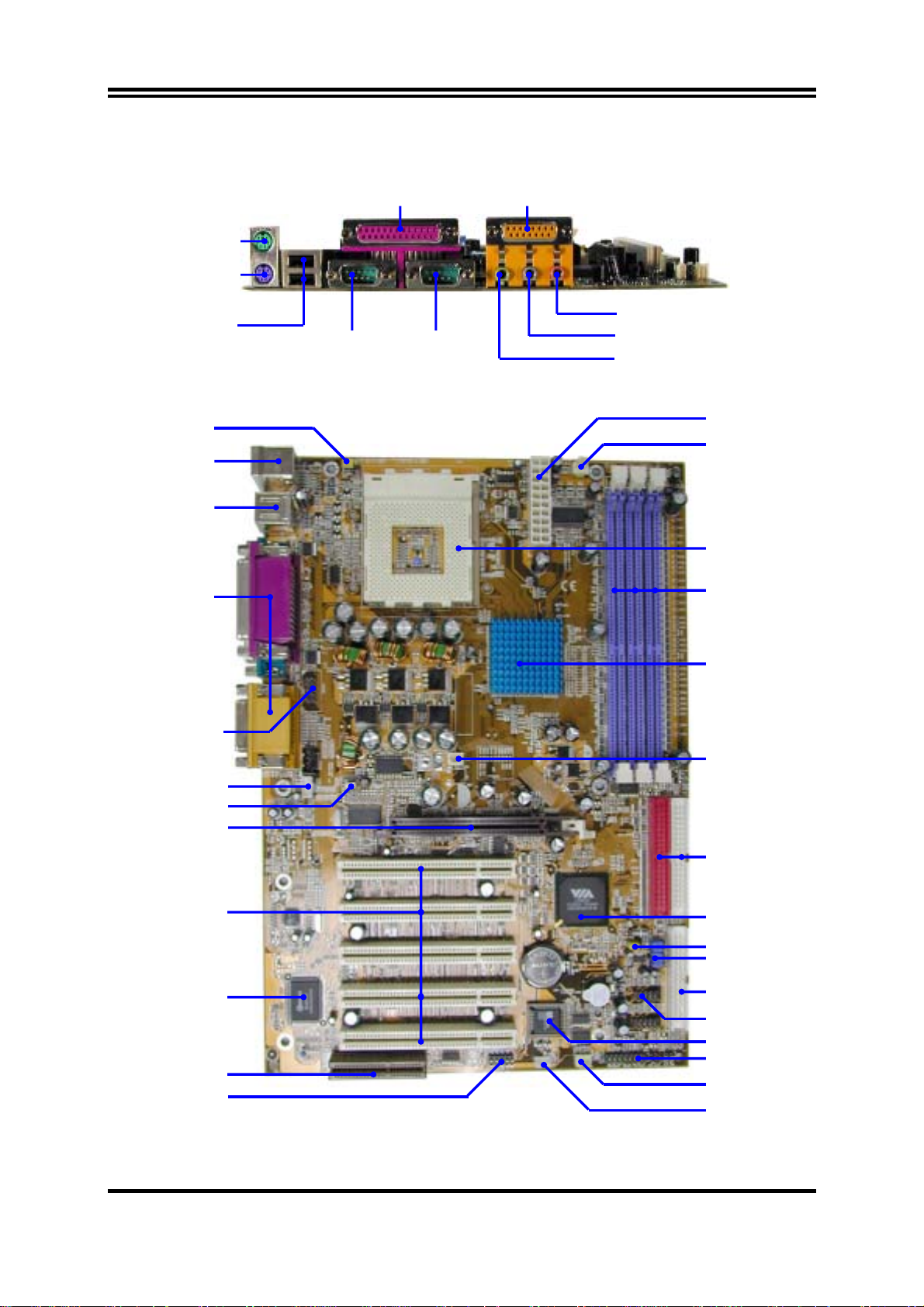
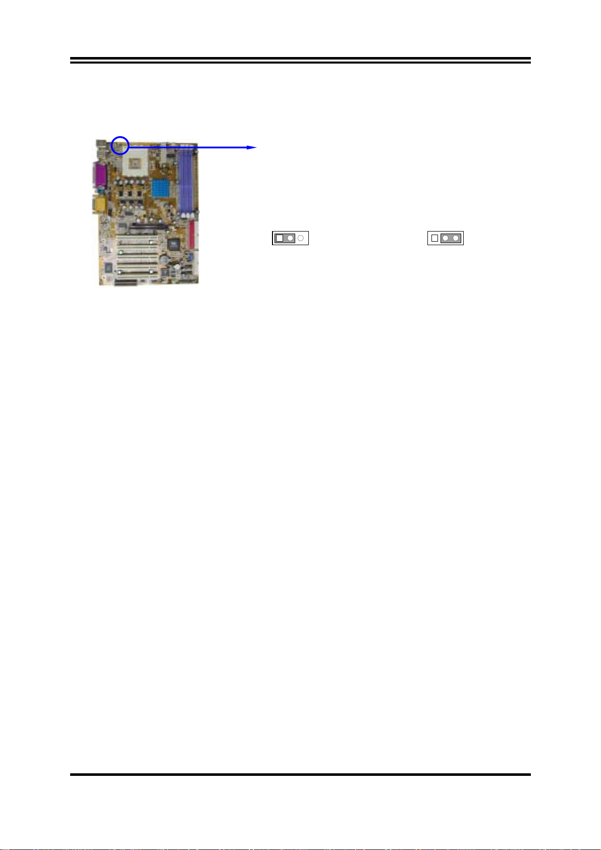
1-4 Layout Diagram & Jumper Setting
PS/2 MOUSE
PRINT GAME/MIDI PORT
PS/2 Keyboard
K/B Power ON
Jumper (JP1)
PS2 KB/Mouse Port
USB Port
PC99 Back Panel
USB
COM1 COM2
MIC
LINE-IN
LINE-OUT
ATX Powe
Connector
CPU FAN
CPU Socket
PC1600/PC2100
DDRX3
VIA KT333 Chip
Front Panel Audio
CD Audio
CPU Front Side Bus
Frequency Jumper (JP4)
AGP Slot
PCI Slot
Winbond 83697HF
Chip
CNR Slot
IR Connector
FAN2
ATA 133 IDE
Connector
VIA VT8233A Chip
Clear CMOS (JBAT)
(JP6)
CPU Ratio Selector
Floppy Connector
USB Port
2MBit Flash ROM BIOS
Front Panel Connector
FAN1
Wake On LAN
6
Page 10
跳線
跳線 名稱 說明 頁碼
JP6
JP4
JBAT
JP1
CPU 倍頻設定
CPU 前端匯流排頻率設定
載入原廠預設之 CMOS 資料
使用鍵盤開機功能設定
10-pin Block P.8
OFF: 133MHz /266MHz
ON : 100MHz /200MHz
3-pin Block P.9
3-pin Block P.9
P.9
連接器
ATXPOWER
J2
J3
PARALLEL
AUD_GAME 音效及遊戲埠介面 3 phone jack + 15-pin Connector P.15
COM1/COM2 串列埠1/串列埠 2 介面 9-pin Connector P.15
FDD 軟碟介面 34-pin Block P.16
IDE1
IDE2
接頭
AUDIO
USB1
IDE LED
TB LED
RESET
SPEAKER
PWR LED
PW BN
WOL
FAN1,FAN2,CPUFAN
IR
CDIN1
連接器 名稱 說明 頁碼
電源介面
PS/2 滑鼠及 PS/2 鍵盤介面
USB 埠介面
並列埠介面
第一個 IDE 介面
第二個 IDE 介面
20-pin Block P.15
6-pin Female P.15
4-pin Connector P.15
25-pin Female P.15
40-pin Block P.16
40-pin Block P.16
接頭 名稱 說明 頁碼
音效輸入/輸出、麥克風連接頭
USB Port 介面
IDE 運轉指示燈
Turbo LED 開關
Reset switch 開關
喇叭線連接頭
電源 LED
電源開關
遠程網路啟動介面
風扇電源接頭
IR 紅外線介面
CD 音效輸入介面
9-pin Block P.17
9-pin Block P.17
2-pin Block P.18
2-pin Block P.18
2-pin Block P.18
4-pin Block P.18
2-pin Block P.18
2-pin Block P.18
3-pin Block P.18
3-pin Block P.19
5-pin Block P.19
4-pin Block P.19
擴充插槽
插座 / 插槽
ZIF Socket 462
DDR1, DDR2, DDR3
PCI1, PCI2, PCI3, PCI4,
PCI5
AGP
名稱 說明 頁碼
CPU 插槽
DDR 記憶體擴充插槽
PCI 插槽
AGP 4X 模式插槽
462-pin PPGA CPU Socket P.11
184-pin DDR Module Expansion Socket P.12
32-bit PCI Local Bus Expansion slots P.13
AGP Expansion Slot P.14
7
Page 11
第二章
硬體安裝
2-1 硬體安裝步驟
在使用你的電腦之前,你必須完成下列步驟:
檢查主機板設定
1.
安裝
2.
3.
4.
5.
6.
7.
CPU 和 CPU
安裝記憶體
安裝擴充卡
連接軟、硬碟排線,面板電線及電源線
設定
BIOS
參數
安裝軟體驅動程式及應用程式
風扇
2-2 檢查主機板的跳線設置
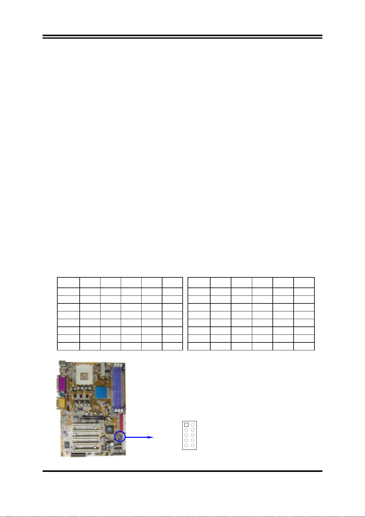
1. CPU
Ratio 1 2 3 4 5 Ratio 1 2 3 4 5
5.0x ON ON ON OFF ON 9.0x ON ON ON OFF OFF
5.5x ON OFF ON OFF ON 9.5x ON OFF ON OFF OFF
6.0x ON ON OFF OFF ON 10.0x ON ON OFF OFF OFF
6.5x ON OFF OFF OFF ON 10.5x ON OFF OFF OFF OFF
7.0X ON ON ON ON OFF 11.0x ON ON ON ON ON
7.5x ON OFF ON ON OFF 11.5x ON OFF ON ON ON
8.0x ON ON OFF ON OFF 12.0x ON ON OFF ON ON
8.5x ON OFF OFF ON OFF 12.5x ON OFF OFF ON ON
倍頻設定
(10-pin) : JP6
JP6
CPU Ratio Selector
1
2
3
4
5
8
Page 12
2. CPU
時脈頻率設定
(2-pin) : JP4
1
2
ON :
BIOS SETUP
中的
Host Clock at Next。
3.
備註
: CPU
時脈頻率設定亦可以經由
37 頁 Miscellaneous Control
清除
CMOS (3-pin) : JBAT
JP4
100MHz/200MHz
CPU Front Side Bus Frequency Setting
主機板必須使用一個電池將主機板的配置資料保存在
將
JBAT 的 1-2
清除
CMOS
關閉系統電源。
1.
並將連接在電源供應器的
2.
將
3.
在
4.
將
5.
時,請依下列步驟:
JBAT
秒鐘後,再將
2~3
電源線重新插回電源供應器上。
AC
備註:什麼時候需要做清除
故障檢修
1.
忘記密碼
2.
超頻時系統無法開機
3.
腳短路來存儲
上的跳帽從
移到
1-2
JBAT
CMOS
電源線拔掉。
AC
2-3
的跳帽移回
CMOS
數據。
的位置。
1-2
的動作:
的位置。
1
JP4
133MHz/266MHz
2
OFF :
程式設定,相關資料請參閱
CMOS RAM
裡,再透過跳帽
鍵盤開機功能設定
4.
: JP1
13
JBAT
1-2 closed Normal
CMOS RAM Clear Setting
9
13
JBAT
2-3 closed Clear CMOS
Page 13
(
)
如果你想使用鍵盤來開機 (按下
取消該功能)。該功能需要一個至少能供應
(
供應器。初始值設為
disable
。
< >)
,請將
設為
JP1
300mA
enable (
電源給
使用該功能),或
+5VSB
引腳的
disable
ATX
電源
1 3
JP1
1-2 closed K/B Power O N Disable
Default
13
JP1
Keyboard Power On Setting
2-3 closed K/B Power O N Enabled
2-3 安裝 CPU
2-3-1 常用術語:
晶片組 (Chipset 亦稱 core logic) – 2 個或以上的積體電路所組成。用於控制系統處理
器、隨機存取記憶體(RAM)、輸出/輸入裝置、擴充卡等等之介面。
處理器插槽 / 插座 (Processor slot/socket) – 主機板上可供中央處理器 (CPU) 嵌入的插
槽或插座。
擴充插槽 (Slot 有 AGP, AMR, PCI, ISA, RAM) – 可讓各式擴充卡或記憶體嵌入的插
槽。目前有 AGP 插槽、AMR 插槽、PCI 插槽、ISA 插槽以及供記憶體使用的 RAM 插
槽等等。
AGP 擴充槽 (Accelerated Graphics Port) – 一種供顯示卡使用的高速介面插槽。目前有
1X (66MHz)、2X (133MHz)、4X (266MHz) 等模式。
PCI 擴充槽 (Peripheral Component Interconnect) – 一種供顯示卡、音效卡、網路卡、數
據機等裝置使用之高速介面插槽;其執行頻率為 33MHz。
ISA 擴充槽 (Industry Standard Architecture) – 一種供舊式音效卡或數據機等裝置使用之
低速介面插槽;其執行頻率約為 8MHz。
串列埠 (Serial Port) – 一種供滑鼠及外接式數據機使用之低速介面連接埠。
並列埠 (Parallel Port) – 一種供印表機使用之低速介面連接埠。
PS/2 – 一種供滑鼠及鍵盤使用之低速介面連接埠。
USB (Universal Serial Bus) – 一種供滑鼠、鍵盤、掃描器、數位照相機使用之中等速度
介面連接埠。
音效裝置 (Sound) – 音效卡或整合於主機板上的音效介面。一般說來,該裝置含有喇叭
接頭、麥克風、搖桿控制介面以及 MIDI 音效裝置。
10
Page 14

區域性網路 (LAN;Local Area Network) – 用於連接區域性網路的介面。
基本輸出/輸入系統 (BIOS;Basic Input/Output System) – 用於系統的啟動和制定不同裝
置彼此間之關係的邏輯程式。
驅動程式(Driver) – 用於定義該裝置之特性,以便其它裝置或軟體使用。
中央處理器(Processor 亦稱 CPU) – 一種用於個人電腦運算之主要的晶片。
前端匯流排頻率
種工作頻率。可供
倍頻
CPU
率。目前大部分之
內部頻率
CPU
(Front Side Bus Frequency)
CPU、DRAM、PCI
(Bus Frequency Ratio)
的倍頻在出廠時即被鎖死,故大部分的主機板已無此設定。
CPU
(CPU Internal Frequency)
: 用於搭配前端匯流排頻率,以計算
率。此一頻率是由前端匯流排頻率
Frequency Ratio)
CPU L2
快取記憶體
Athlon CPU
所計算出來。
的內部有
(CPU L2 Cache)
256K
或更高,而
匯流排使用。
(Front Side Bus Frequency)
:一種位於
Duron
:經由主機板上之時脈產生器所產生的一
:
的內部頻率,亦是
CPU
內部的快取記憶體。一般說來,
CPU
則為
64K。
2-3-2 關於 AMD Athlon & Duron 462-腳位 CPU
此主機板提供了一個
止
警告 !
過熱。 如果你尚未購買風扇,請在安裝系統前請購買一個合適的風扇。
CPU
請確保處理器之散熱片的表面有充足的空氣流通,且
工作正常。否則將使處理器和主機板因過熱而造成損壞。如果需要
的話,你可以另外安裝輔助風扇。
ZIP Socket-A
的插座。安裝在主機板上的
乘以
CPU
CPU
實際的工作頻
CPU
CPU
工作頻
倍頻
(Bus
必須裝有風扇以防
冷卻風扇
CPU
警告
安裝
!
CPU
因為此主機板提供有
FAN1
系統電源關閉以保護你的
前,先請關閉你的系統再移除外殼。找到
使之向上成90度。將
的末端。因為
四個角中有兩角缺了一個引腳,因此會適合於如圖所示的方位。
CPU
CPU
的位置。如果未將風扇電源接在
從如下圖所示的正確方位插入。有凹口的一角應該朝向拉桿
CPU
過熱保護裝置,請務必將
的位置,主機板會馬上將
插槽並先從插槽一側拉起拉桿
CPU
FAN1
和主機板。
ZIF
CPU
風扇電源接在
11
Page 15

Socket-A
Colden Arrow
AMD
當你將
CPU
按下即可。
插入
插槽時,不要使用太大的力量,插入後只要輕輕把拉桿沿正確方向
ZIF
CPU ZIF Socket-A
2-4 安裝記憶體
此主機板提供有 三條
體從最小的
64MB
有效記憶體配置
Bank 184-Pin DIMM Total Memory
Bank 0, 1 (DDR1) PC1600/PC2100/PC2700 DDR SDRAM X1 64MB∼1.0GB
Bank 2, 3 (DDR2) PC1600/PC2100/PC2700 DDR SDRAM X1 64MB∼1.0GB
Bank 4, 5 (DDR3) PC1600/PC2100/PC2700 DDR SDRAM X1 64MB∼1.0GB
Total System Memory (Max. 3.0GB) 3 64MB∼3.0GB
184-pin DUAL INLINE MEMORY MODULES (DIMM)
擴充至最大的
3.0GB
記憶體。
可使記憶
注意
請確認所使用之記憶體總容量沒有超過
!
進而導致系統不開機之狀態。
3.0GB
,否則容易造成系統誤判,
一般說來,將記憶體安裝到主機板上是非常容易的,你可以參考圖
簡圖。
注意!
當你將
DIMM
記憶體完全插入
卡好,使其恰好卡住兩端的凹口。
DDR2 (BANK2+ BANK3)
DDR1 (BANK0+ BANK1)
DDR3 (BANK4+ BANK5)
Figure 2-4
DIMM
插槽時,請將兩端的白色護耳緊緊地
安裝記憶體的
2-4
12
Page 16

警告!
如果
組。當此主機板設成
會由於嚴格的時脈問題,導致系統無法啟動。如有這種現象,請將
SDRAM
2-5 擴充卡
警告!
當添加、移除擴充卡,或其他系統組件時務必請關掉電源,以避免對主
機板和擴充卡造成損害。
DDR SDRAM
的頻率設為
頻率設為
133MHz
100MHz
166MHz
時,如果您的
以確保系統的穩定性。
時,祇能使用
DDR
PC2700
不是
PC2100
相容的
相容的話,
DDR
DDR
模
2-5-1 擴充卡安裝程序
仔細閱讀擴充卡所附之文件,將所有相關之必要的軟、硬體設定好,比如跳線。
1.
移除電腦外殼,並將你想要安裝之插槽處的金屬支架拆除。
2.
將該擴充卡插入並穩固地壓下去。
3.
鎖上螺絲。
4.
將系統機殼放回原位。
5.
如果有必要,請在
6.
安裝擴充卡所須的相關驅動程式。
7.
內設定其參數。
BIOS
2-5-2
某些擴充卡需要指定
定給某一個裝置使用。在標準設計中,有16個
統使用中。
IRQ
設定擴充卡的 IRQ
方可使用。一般來說,每一個
IRQ
是可用的,但其中的大部分都已被系
IRQ
的基本中斷分配表
IRQ Priority Standard function
0 N/A System Timer
1 N/A Keyboard Controller
2 N/A Programmable Interrupt
3 * 8 Communications Port (COM2)
4 * 9 Communications Port (COM1)
5 * 6 Sound Card (sometimes LPT2)
的埠口位址祇能單獨地指
IRQ
13
Page 17

6 * 11 Floppy Disk Controller
7 * 7 Printer Port (LPT1)
8 N/A System CMOS/Real Time Clock
9 * 10 ACPI Mode when enabled
10 * 3 IRQ Holder for PCI Steering
11 * 2 IRQ Holder for PCI Steering
12 * 4 PS/2 Compatible Mouse Port
13 N/A Numeric Data Processor
14 * 5 Primary IDE Channel
15 * 1 Secondary IDE Channel
上述的
*
IRQ
通常可供
ISA 或 PCI
介面裝置使用。
2-5-3 主機板的中斷列表
主機板共用的中斷指令如下表所示:
INT A INT B INT C INT D
PCI slot 1 Shared
PCI slot 2
PCI slot 3
PCI slot 4
PCI slot 5 Shared
AGP slot Shared
AC97/MC97
Onboard USB
Onboard USB 1
Onboard USB 2 Shared
Shared
Not Shared
Shared
Shared
Shared
Shared
注意事項 !
如果你在共用的插槽上使用
或者該卡不需要分配任何
IRQ”
突,進而使得整個系統不穩定而且
2-5-4 AGP 插槽
此主機板提供有一個可支援
1X/2X/4X
模式的
14
卡,請確認驅動程式可支援
PCI
IRQ
顯示卡插槽。
AGP
。否則
PCI
兩個
PCI
卡將不可使用。
”Shared
組之間將產生衝
Page 18

2-6 連接埠,接頭
2-6-1 連接埠 (Connectors)
電源介面
(1)
此為
由個人電腦面板上一個
(20-pin block) : ATXPOWER
ATX
電源供應器的介面,其
2-pin
20-pin
的開關控制。
AGP SLOT
的定義如下表。
電源供應器電源經
ATX
(2) PS/2
滑鼠及
滑鼠介面可連接
PS/2
當您的配備不是
(3) USB
(4)
埠介面
該
USB
並列埠介面
埠可讓兩個
(25-pin female): PARALLEL
PS/2
PS/2
: J3
鍵盤介面
規格,則需經由轉接器式轉接排線,接到主機板。
USB
PIN ROW2 ROW1
1 3.3V 3.3V
2 -12V 3.3V
3 GND GND
4 Soft Power On 5V
5 GND GND
6 GND 5V
7 GND GND
8 -5V Power OK
9 +5V +5V (for Soft Logic)
10 +5V +12V
Pin 1
: J2
PS/2
滑鼠,同樣地,
裝置連接到主機板。
15
鍵盤介面也用於連接
PS/2
鍵盤,
PS/2
Page 19

該並列埠介面為一個25針母頭構成,可於
料請參閱第三章的
音效及遊戲介面
(5)
“INTEGRATED PERIPHERALS SETUP”。
: AUD_GAME
音效介面有輸出、輸入、麥克風、搖桿四個介面。
輸出:
輸入:
麥克風: 由麥克風輸入
遊戲介面:是一個
音效輸出至喇叭
音效輸入至音效晶片
15-pin 的D
型母頭,可連接搖桿或
BIOS
設定中
MIDI
disable
裝置
該並列埠。詳細資
串列埠介面
(6)
COM1 和 COM2
enable
。詳細資料請參閱第三章的
: COM1, COM2
是一個
9-pin D
型公頭,該串列埠可經由
BIOS
設定為
“INTEGRATED PERIPHERAL S SETUP”。
disable 或
PS/2
MOUSE
PRINT GAME/MIDI PORT
軟碟介面
(7)
該介面經由一條
(34-pin block): FDD
PS/2
Keyboard
34-pin
USB
COM1 COM2
排線與軟碟連接,一般來說,排線有紅邊的方向與
相應,所以在裝置排線時應將紅邊對應軟碟介面的
Floppy Drive Connector
第一個
(8)
該介面經由一條
品所附的
介面
IDE
ATA-133
(40-pin block): IDE1
40-pin
排線與硬碟連接,同樣地,也是紅邊對介面
排線可讓你用於連接
Pin 1
ATA-133
Pin 1
硬碟。
方向。
MIC
LINE-IN
LINE-OUT
Pin 1
Pin 1
,本產
16
Page 20

Pin 1
Primary IDE Connector
第二個
(9)
該介面為另一個
IDE
介面
(40-pin block): IDE2
裝置介面,同樣可經由排線連接兩個
IDE
IDE
裝置。
Pin 1
每個連接埠能連接兩個硬碟。第一個
•
Secondary IDE Connector
HDD
相當於
“Master”,
第二個
HDD
“Slave”。
為了性能的考慮,我們強烈建議請不要將
•
裝在同一個
通道上。否則,此通道上的系統性能將會降低。
IDE
CD-ROM或DVD-ROM
驅動器與硬碟安
2-6-2 接頭 (Headers)
音效輸出/輸入及麥克風接頭
(1)
如果你的電腦機殼有前面板音效輸出/輸入及麥克風排線,可將排線接到此接頭。
(9-pin): AUDIO
相當於
17
Page 21

A
L
L
L
(2) USB Port
介面
(9-pin) : USB1
這兩個接頭是用來連接附加的
線,即可使用附於面板上的兩個額外
(3) IDE
運轉指示燈
: IDE LED
將硬碟運轉指示燈連接到電腦機殼的接頭。
L-I N-L
MIC
-O UT-
Line-In/Out, MIC Headers
USB
Pin 1
UDIO
L-I N-R
MICP
GND
-OUT-R
介面插頭。透過各外加一條可選購的
插頭。
USB
USB1
Pin 1
USB Port Connector
VCC
DATA
-
VCC
DATA
-
GND
+ DATA
GND
GND
+ DATA
(4) Turbo LED
開關
: TB LED
主機板加速開關的預設值為"開啟" 狀態。當系統電源開啟時,加速燈會一直亮
著。你也可以將電腦機殼的電源
連接到這裡,表示電源開或關的顯示。
LED
(5) Reset
這個
情況下重啟電腦的目的。
開關
2-pin
: RESET
接頭可連接電腦機殼上「
」的電源線,以達到不關閉系統電源的
reset
喇叭連線開關
(6)
這個
4-pin
: SPEAKER
接頭可連接電腦機殼上「
speaker
」的開關,以供機殼上的喇叭使用。
電源
(7)
你可將電腦機殼上的
LED
開關
LED
: PWR LED
的燈就會亮起來。
Power LED
線連到此一開關,當系統電源開啟時,
電源開關
(8)
這個
: PW BN
2-pin
接頭可連接電腦機殼上的電源開關,供電腦啟動或關閉使用。
USB
Power
排
18
Page 22

Tur bo SW
Power LE D
GND
NC
VCC
GND
Speaker
System Case Connections
遠程網路啟動介面
(9)
將具有
WAKE ON LAN
(3-pin) : WOL
輸出規格的網路卡與該介面連接後,當網路卡收到啟動訊
號時即可啟動系統,達到遠端程式控制目的。
備註: 使用此一功能前,請確定 BIOS 中的
已設定成
enabled
狀態。
NC
VCC
VCC
GND
PW BN
IDELED
GND
GND
Reset SW
Turbo L ED
Wake On LAN 或 Ring In Wake up
風扇電源接頭
(10)
這些介面支援
(3-pin) : FAN1, FAN2, CPUFAN
350mA (4.2 瓦)
WOL
Wake-On-LAN Headers
或以下的冷卻風扇,根據風扇生產廠商的不同,電
5VS B
GND
WON
線和插座也會不同。紅線應當是陽極,而黑線則是接地。將風扇接頭插到主機板
時,應考慮連接頭的極性。
19
Page 23

1
3
13
13
CPUFAN
FAN2
FAN1
(11) IR
紅外線介面
(9-pin) : IR
該介面支援可選購的紅外線無線傳輸以及接收組件。必須在
參數以使用
的功能。
IR
NC
CIRRX
VCC
NC
IOVSB
10
CIR: (Pin6∼Pin10) for Consumer IR
5
IR: (Pin1∼Pin5) for Standard IR
GND
IRRX
IRTX
NC
CIR
6
IR
1
Infrared Module Headers
(12) CD
音效輸入介面
CDIN1 是 CD
(4-pin) : CDIN1
音效輸入訊號介面,可與
CD-ROM
BIOS setup
音效輸出連接。
中設定其
CDI N1
CD Audio-In Headers
4
1
2-7 啟動你的電腦
所有排線都接好之後,蓋上機殼。
1.
請確認所有的開關都是關閉的,然後檢查電源的輸出電壓是否設為正確位置,通常情況下
2.
輸入電壓為
220V∼240V或 110V∼120V
,這取決於你所處位置的使用電壓。
20
Page 24

依照你系統的使用手冊,將電源線連接到位於機殼後部的電源接頭上。
3.
依照下列順序將週邊設備依次打開:
4.
顯示器。
a.
其他週邊設備 (印表機,掃描器,外接式數據機等等
b.
系統電源。在
c.
殼前面的
ATX
ATX
電源,你必須先打開電源供應器後方電源開關,然後按下位於機
電源開關。
。
…
)
位於機殼前面的電源
5.
求,或具有電源待機特性。當系統啟動後在桔紅色與綠色之間切換,接著系統將執行自我
檢測。自我檢測執行時,
如果從開啟電源起的30秒內沒看到任何動靜,系統則可能已經自我檢測失敗。請再次檢查
你的跳線設定以及連接設定或是打電話向你的零售商尋求協助。
自我檢測響鈴
顯示
不停地響
一聲長響後三聲短響
系統工作時發出高頻率響聲
在電腦啟動其間,如果需要更改
6.
BIOS setup
關閉你的電腦: 在關閉電源開關之前,你必須先關閉你的操作系統。如果你是用
7.
電源供應器,在退出或關閉操作系統後可以按下電源開關。如果你使用的操作系統是
Windows 9X
Windows
後一短響
logo
,再依照
版本,按下 “開始” 按鈕,再按“關機”,然後按“關閉這台電腦
在關閉相關應用程式後,會自動關掉電源。
將會點亮。顯示器的
LED
將發出嘟嘟聲,同時將相關提示資訊顯示在螢幕上。
BIOS
CPU
BIOS SETUP
會亮起,如果系統符合綠色環保省電要
LED
意義
系統啟動正常
未安裝或未檢測到
未找到顯示卡或顯示用快取記憶體損壞
過熱
系統處於低頻工作環境
BIOS
的線上指示完成相關設定。
設定之任何參數,只要按下
DRAM
<Delete>
鍵即可進入
ATX
(S)”
的
,
第三章
BIOS 介紹
是一段儲存在快讀寫式記憶體
BIOS
(FLASH ROM)
是主機板與操作系統間的一架橋樑。電腦啟動時,會先由
執行一個稱為
POST
(開機自我檢測)的自我測試,它會偵測所有硬體設備,並確認同
步硬體參數。當完成所有檢測時,它才將系統的控制權移交給操作系統(OS)。由於
是硬體與軟體聯繫的唯一通道,所以是系統穩定性的關鍵因素,進而確保系統性
BIOS
能可達到最佳狀態。
如圖
3-1
所示,在
設定程式主目錄中,可看到一些選項。我們將在本章的後面逐
BIOS
步解釋這些選項,首先讓我們先看看你將在此用到之功能鍵的簡單描述:
之基本輸出、入控制程式。該程式
BIOS
程式進行控制 。 首先
21
Page 25

•
按
<Esc>
鍵,可退出
BIOS
設定程式。
按
•
•
•
↑↓←→
選項。
當你想要對選項進行參數設定時請按
當完成對參數的設定後,請按
式,同時電腦也會自動重新開機。
向上,向下,向左,向右) 鍵,可在主目錄中選擇你想確認或修改的
(
鍵。
–
BIOS
設定程
<F10>
Page Up/Page Down 或+/
鍵,儲存修改的參數並退出
3-1 進入 Setup
在啟動電源開關並且按住
中按下
<Del>
鍵順利進入
<Del>
CMOS SETUP
關,或者是直接按下電腦機殼上的
<Alt> 和<Delete>
鍵來以重新啟動電腦,並再按
按下以上所有的鍵,或者系統重新啟動失敗,此時在螢幕上會顯示錯誤訊息如下:
Press <F1> to continue, <Ctrl-Alt-Esc> or <Del> to enter Setup
你可按
鍵繼續,或按
<F1>
就可以馬上進入
,那麼可以透過把電源關掉,然後再打開電源開
“RESET”
<Ctrl-Alt-Esc>
Setup
程式。如果你來不及在
按鈕重啟動系統,還是同時按下
鍵試一次。如果沒能在正確時間內
Del
組合鍵重新啟動電腦,還是按
POST
<Ctrl>,
<Del>
過程
鍵,進入
BIOS
設定程式。
3-2 線上說明
主目錄
所選取之設定功能的說明,會以反白方式顯示在螢幕底部。
狀態頁安裝目錄/選項頁安裝目錄
按
能的選擇。再按
鍵,則會彈出一個線上說明的小視窗,該視窗描述了該選項中可用之指令以及可
F1
<Esc>
鍵,則可退出該線上說明視窗。
3-3 主目錄
22
Page 26

一旦你進入
項設定功能選項和兩項退出選項中加以選擇。請使用方向鍵在各選項之間進行選
14
擇,再按
Award BIOS CMOS Setup
<Enter>
CMOS Setup Utility – Copyright(C) 1984-2001 Award Software
鍵接受或是進入子目錄。
,主目錄(圖
)會顯示在螢幕中。你可以從
3-1
Standard CMOS Features
Advanced BIOS Features
Advanced Chipset Features
Integrated Peripherals
Power Management Setup
PnP/PCI Configurations
PC Health Status
Esc : Quit
F10 : Save & Exit Setup
Time, Date, Hard Disk Type...
Figure 3-1
Miscellaneous Control
Load optimized Defaults
Load Standard Defaults
Set Supervisor Password
Set User Password
Save & Exit Setup
Exit Without Saving
↑↓→ ←
: Select Item
Standard CMOS Features
CMOS
的標準設定。
Advanced BIOS Features
特性的進階設定。
BIOS
Advanced Chipset Features
晶片組參數的進階設定,透過更改其設定之參數,可提高系統性能。
Integrated Peripherals
周邊配備設定。
Power Management Setup
電源管理的設定。
PnP/PCI configurations
(即插即用)與
PnP
匯流排的組態設定。
PCI
PC Health Status
該項目顯示系統狀態,如
CPU
溫度、風扇轉速等等。
Miscellaneous Control
該項目可讓你指定其它相關控制的設定。
23
Page 27

Load Optimized Defaults
載入最佳化設定。
Load Standard Defaults
載入原廠的預設值。
Set Supervisor/User Password
設定監督者/使用者密碼。
Save & Exit Setup
儲存
CMOS
的設定,然後退出
Setup
程式。
Exit Without Saving
放棄
CMOS
所有的修改,然後退出
Setup
程式。
3-4 Standard CMOS Features
The items in Standard CMOS Setup Menu are divided into several categories. Each category
includes no, one or more than one setup items. Use the arrow keys to highlight the item and
then use the <PgUp> or <PgDn> keys to select the value you want in each item.
CMOS Setup Utility – Copyright(C) 1984-2001 Award Software
Standard CMOS Features
Date (mm:dd:yy) Thu, Jul, 05 2001
Time (hh:mm:ss) 11 : 33 : 50
> IDE Primary Master Press Enter None
> IDE Primary Slave Press Enter None
> IDE Secondary Master Press Enter None
> IDE Secondary Slave Press Enter None
Drive A 1.44M, 3.25 in.
Drive B None
Video EGA/VGA
Halt On All,But Keyboard
Base Memory 640K
Extended Memory 56320K
Total Memory 57344K
Item Help
Menu Level >
Change the day, month,
year and century
Date
↑↓→←
Move Enter:Select +/-/PU/PD:Value F10:Save ESC:Exit F1:General Help
F5:Previous Values F6:Optimized Defaults F7:Standard Defaults
24
Page 28

The date format is <day><month><date><year>.
Day of the week, from Sun to Sat, determined by BIOS. Read-only.
Day
Month
Date
Year
The month from Jan. through Dec.
The date from 1 to 31 can be keyed by numeric function keys.
The year depends on the year of the BIOS.
Time
The time format is <hour><minute><second>.
Primary Master/Primary Slave
Secondary Master/Secondary Slave
Press PgUp/<+> or PgDn/<–> to select Manual, None, Auto type. Note that the specifications
of your drive must match with the drive table. The hard disk will not work properly if you
enter improper information for this category. If your hard disk drive type is not matched or
listed, you can use Manual to define your own drive type manually.
If you select Manual, related information is asked to be entered to the following items. Enter
the information directly from the keyboard. This information should be provided in the
documentation from your hard disk vendor or the system manufacturer.
If the controller of HDD interface is SCSI, the selection shall be “None”.
If the controller of HDD interface is CD-ROM, the selection shall be “None”
Access Mode
Cylinder
Head
Precomp
Landing Zone
Sector
number of sectors
The settings are Auto Normal, Large, and LBA.
number of cylinders
number of heads
write precomp
landing zone
3-5 Advanced BIOS Features
CMOS Setup Utility – Copyright(C) 1984-2001 Award Software
Advanced BIOS Features
Anti-Virus Protection Disabled
Recovery Genius Enabled
25
Item Help
Page 29

PhoneixNet Support Disabled
CPU L1 Cache Enabled
CPU L2 Cache Enabled
Quick Power On Self Test Enabled
ATA & SCSI Boot Order ATA, SCSI
First Boot Device Floppy
Second Boot Device HDD-0
Third Boot Device CDROM
Boot other Device Enabled
Swap Floppy Drive Disabled
Boot Up Floppy Seek Enabled
Boot Up NumLock Status On
Gate A20 Option Normal
Typematic Rate Setting Disabled
Typematic Rate (Chars/Sec) 6
Typematic Delay (Msec) 250
Security Option Setup
OS Select For DRAM > 64MB Non-OS2
HDD S.M.A.R.T. Capability Disabled
Video BIOS Shadow Enabled
↑↓→←
Move Enter:Select +/-/PU/PD:Value F10:Save ESC:Exit F1:General Help
F5:Previous Values F6:Optimized Defaults F7:Standard Defaults
Menu Level >
Anti-Virus Protection
Allows you to choose the VIRUS Warning feature for IDE Hard Disk boot sector protection.
If this function is enabled and someone attempt to write data into this area, BIOS will show a
warning message on screen and alarm beep.
Disabled
(default) No warning message to appear when anything attempts to access the
boot sector or hard disk partition table.
Enabled
Activates automatically when the system boots up causing a warning
message to appear when anything attempts to access the boot sector of
hard disk partition table.
CPU Internal Cache
The default value is Enabled.
Enabled
Disabled
(default) Enable cache
Disable cache
Note: The internal cache is built in the processor.
External Cache
Choose Enabled or Disabled. This option enables the Level 2 cache memory.
CPU L2 Cache ECC Checking
Choose Enabled or Disabled. This option enables the Level 2 cache memory ECC (error
check correction).
Quick Power On Self-Test
This category speeds up Power On Self Test (POST) after you power on the computer. If this
is set to Enabled. BIOS will shorten or skip some check items during POST.
Enabled
Disabled
(default) Enable quick POST
Normal POST
26
Page 30

First/Second/Third/Fourth Boot Device
The BIOS attempts to load the operating system from the devices in the sequence selected in
these items. The settings are Floppy, LS/ZIP, HDD-0/HDD-1/HDD-3, SCSI, CDROM, LAD
and Disabled.
Swap Floppy Drive
Switches the floppy disk drives between being designated as A and B. Default is Disabled.
Boot Up Floppy Seek
During POST, BIOS will determine if the floppy disk drive installed is 40 or 80 tracks. 360K
type is 40 tracks while 760K, 1.2M and 1.44M are all 80 tracks.
Boot Up NumLock Status
The default value is On.
(default)
On
Off
Keypad is numeric keys.
Keypad is arrow keys.
Gate A20 Option
Normal
(default) The A20 signal is controlled by port 92 or chipset specific method.
Fast
The A20 signal is controlled by keyboard controller or chipset hardware.
Typematic Rate Setting
Keystrokes repeat at a rate determined by the keyboard controller. When enabled, the
typematic rate and typematic delay can be selected. The settings are: Enabled/Disabled.
Typematic Rate (Chars/Sec)
Sets the number of times a second to repeat a keystroke when you hold the key down. The
settings are: 6, 8, 10, 12, 15, 20, 24, and 30.
Typematic Delay (Msec)
Sets the delay time after the key is held down before is begins to repeat the keystroke. The
settings are 250, 500, 750, and 1000.
Security Option
This category allows you to limit access to the system and Setup, or just to Setup.
System
The system will not boot and access to Setup will be denied if the
correct password is not entered at the prompt.
Setup
(default) The system will boot, but access to Setup will be denied if the correct
password is not entered prompt.
OS Select For DRAM > 64MB
Allows OS2 to be used with >64MB or DRAM. Settings are Non-OS/2 (default) and OS2.
Set to OS/2 if using more than 64MB and running OS/2.
3-6 Advanced Chipset Features
The Advanced Chipset Features Setup option is used to change the values of the chipset
registers. These registers control most of the system options in the computer.
27
Page 31

CMOS Setup Utility – Copyright(C) 1984-2001 Award Software
Advanced Chipset Features
> DRAM Timing Settings Press Enter
> AGP Timing Settings Press Enter
> PCI Timing Settings Press Enter
System BIOS Cacheable Disabled
Video RAM Cacheable Disabled
Memory Hole Disabled
↑↓→←
Move Enter:Select +/-/PU/PD:Value F10:Save ESC:Exit F1:General Help
F5:Previous Values F6:Optimized Defaults F7:Standard Defaults
Item Help
Menu Level >
DRAM Timing Settings
Please refer to section 3-6-1
AGP Timing Settings
Please refer to section 3-6-2
PCI Timing Settings
Please refer to section 3-6-3
System BIOS Cacheable
Selecting Enabled allows caching of the system BIOS ROM at F0000h-FFFFFh, resulting in
better system performance. However, if any program writes to this memory area, a system
error may result. The settings are: Enabled and Disabled.
Video RAM Cacheable
Select Enabled allows caching of the video BIOS, resulting in better system performance.
However, if any program writes to this memory area, a system error may result. The settings
are: Enabled and Disabled.
Memory Hole
You can reserve this area of system memory for ISA adapter ROM. When this area is
reserved, it cannot be cached. The user information of peripherals that need to use this area of
system memory usually discusses their memory requirements. The settings are: Enabled and
Disabled.
3-6-1 DRAM Timing Settings
CMOS Setup Utility – Copyright(C) 1984-2001 Award Software
DRAM Timing Settings
28
Page 32

Auto Configuration Optimized
RAS Active Time 6T
RAS Precharge Time 3T
RAS to CAS Delay 3T
CAS Latency 2.5T
Bank Interleave 4 Bank
DRAM Command Rate 2T Command
Item Help
Menu Level >>
↑↓→←
Move Enter:Select +/-/PU/PD:Value F10:Save ESC:Exit F1:General Help
F5:Previous Values F6:Optimized Defaults F7:Standard Defaults
RAS Active Time
This field let’s you insert a timing delay between the CAS and RAS strobe signals, used when
DRAM is written to, read from, or refreshed. Fast gives faster performance; and Slow give s
more stable performance. This field applies only when synchronous DRAM is installed in the
system. The settings are: 2T and 3T.
RAS Precharge Time
If an insufficient number of cycles is allowed for the RAS to accumulate its charge before
DRAM refresh, the refresh may be incomplete and the DRAM may fail to retain date. Fast
gives faster performance; and Slow gives more stable performance. This field applies only
when synchronous DRAM is installed in the system. The settings are: 2T and 3T.
CAS Latency
When synchronous DRAM is installed, the number of clock cycles of CAS latency depends
on the DRAM timing. The settings are: 2T and 2.5T.
3-6-2 AGP Timing Settings
CMOS Setup Utility – Copyright(C) 1984-2001 Award Software
AGP Timing Settings
AGP Transfer Aperture Size 64M
AGP Mode Auto
AGP Driving Control Auto
AGP Driving Value DA
AGP Fast Write Disabled
AGP Master 1 WS Write Enabled
AGP Master 1 WS Read Enabled
CPU to AGP Post Write Disabled
AGP Delay Transaction Disabled
Item Help
Menu Level >>
↑↓→←
Move Enter:Select +/-/PU/PD:Value F10:Save ESC:Exit F1:General Help
F5:Previous Values F6:Optimized Defaults F7:Standard Defaults
Note: Change these settings only if you are familiar with the chipset.
3-6-3 PCI Timing Settings
CMOS Setup Utility – Copyright(C) 1984-2001 Award Software
PCI Timing Settings
29
Page 33

PCI Master 1 WS Write Disabled
PCI Master 1 WS Read Disabled
CPU to AGP Post Write Disabled
PCI Delay Transaction Disabled
↑↓→←
Move Enter:Select +/-/PU/PD:Value F10:Save ESC:Exit F1:General Help
F5:Previous Values F6:Optimized Defaults F7:Standard Defaults
Item Help
Menu Level >>
PCI Delay Transaction
The chipset has an embedded 32-bit posted write buffer to support delay transactions cycles.
Select Enabled to support compliance with PCI specification version 2.1. The settings are:
Enabled and Disabled.
3-7 Integrated Peripherals
CMOS Setup Utility – Copyright(C) 1984-2001 Award Software
Integrated Peripherals
> OnChip IDE Function Press Enter
> OnChip Device Function Press Enter
> Onboard Super IO Function Press Enter
Init Display First PCI Slot
↑↓→←
OnChip IDE Function
Please refer to section 3-7-1
OnChip Device Function
Please refer to section 3-7-2
Onboard Super IO Function
Please refer to section 3-7-3
Move Enter:Select +/-/PU/PD:Value F10:Save ESC:Exit F1:General Help
F5:Previous Values F6:Optimized Defaults F7:Standard Defaults
Item Help
Menu Level >
Init Display First
This item allows you to decide to activate whether PCI Slot or AGP VGA first. The settings
are: PCI Slot, AGP Slot.
3-7-1 OnChip IDE Function
CMOS Setup Utility – Copyright(C) 1984-2001 Award Software
OnChip IDE Function
30
Page 34

OnChip IDE Channel0 Enabled
OnChip IDE Channel1 Enabled
Primary Master PIO Auto
Primary Slave PIO Auto
Secondary Master PIO Auto
Secondary Slave PIO Auto
Primary Master UDMA Auto
Primary Slave UDMA Auto
Secondary Master UDMA Auto
Secondary Slave UDMA Auto
IDE 32-bit Transfer Mode Enabled
IDE HDD Block Mode Enabled
IDE Prefetch Mode Enabled
Delay For HDD (Secs) 0
Item Help
Menu Level >>
↑↓→←
Move Enter:Select +/-/PU/PD:Value F10:Save ESC:Exit F1:General Help
F5:Previous Values F6:Optimized Defaults F7:Standard Defaults
OnChip IDE Channal0/Channel1
The integrated peripheral controller contains an IDE interface with support for two IDE
channels. Select Enabled to activate each channel separately. The settings are: Enabled and
Disabled.
Primary/Secondary Master/Slave PIO
The four IDE PIO (Programmed Input/Output) fields let you set a PIO mode (0-4) for each of
the four IDE devices that the onboard IDE interface supports. Modes 0 through 4 provide
successively increased performance. In Auto mode, the system automatically determines the
best mode for each device. The settings are: Auto, Mode 0, Mode 1, Mode 2, Mode 3, Mode
4.
Primary/Secondary Master/Slave UDMA
Ultra DMA/33 implementation is possible only if your IDE hard drive supports it and the
operating environment includes a DMA driver (Windows 95 OSR2 or a third-party IDE bus
master driver). If your hard drive and your system software both support Ultra DMA/33 and
Ultra DMA/66, select Auto to enable BIOS support. The settings are: Auto, Disabled.
IDE HDD Block Mode
Block mode is also called block transfer, multiple commands, or multiple sector read/write. If
your IDE hard drive supports block mode (most new drives do), select Enabled for automatic
detection of the optimal number of block read/writes per sector the drive can support. The
settings are: Enabled, Disabled.
3-7-2 OnChip Device Function
CMOS Setup Utility – Copyright(C) 1984-2001 Award Software
OnChip Device Function
31
Page 35

AC97 Sound Device Auto
Game Port Address 201
Midi Port Address Disabled
Midi Port IRQ 10
AC97 Modem Device Auto
USB Host Controller Enabled
USB Keyboard Legacy Support Disabled
↑↓→←
Move Enter:Select +/-/PU/PD:Value F10:Save ESC:Exit F1:General Help
F5:Previous Values F6:Optimized Defaults F7:Standard Defaults
Item Help
Menu Level >>
AC97 Sound Device
This item allows you to decide to enable/disable the KT266A chipset family to support AC97
Audio. The settings are: Enabled, Disabled.
Game Port Address/Midi Port Address
This will determine which Address the Game Port/Midi Port will use.
AC97 Modem Device
This item allows you to decide to enable/disable the KT266A chipset family to support AC97
Modem. The settings are: Auto, Disabled.
USB Host Controller
Select Enabled if your system contains a Universal Serial Bus (USB) controller and you have
a USB peripherals. The settings are: Enabled, Disabled.
USB Keyboard Support
Select Enabled if your system contains a Universal Serial Bus (USB) controller and you have
a USB keyboard. The settings are: Enabled, Disabled.
3-7-3 Onboard Super IO Function
CMOS Setup Utility – Copyright(C) 1984-2001 Award Software
Onboard Super IO Function
Onboard FDD Controller Enabled
Onboard Serial Port 1 3F8/IRQ4
Onboard Serial Port 2 2F8/IRQ3
UART2 Mode Normal
RxD, TxD Active Hi, Lo
IR Duplex Mode Half
Use IR Pins IRRX/IRTX
Onboard Parallel Port 378/IRQ7
Parallel Mode SPP
EPP Mode Select EPP1.9
ECP Mode Use DMA 3
Item Help
Menu Level >>
↑↓→←
Move Enter:Select +/-/PU/PD:Value F10:Save ESC:Exit F1:General Help
F5:Previous Values F6:Optimized Defaults F7:Standard Defaults
Onboard FDD Controller
32
Page 36

Select Enabled if your system has a floppy disk controller (FDD) installed on the system board
and you wish to use it. If you install add-on FDC or the system has no floppy drive, select
Disabled in this field. The settings are: Enabled and Disabled.
Onboard Serial Port 1/Port 2
Select an address and corresponding interrupt for the first and the second serial ports. The
settings are: 3F8/IRQ4, 2E8/IRQ3, 3E8/IRQ4, 2F8/IRQ3, Disabled, Auto.
UART2 Mode
This item allows you to determine which InfraRed(IR) function of the onboard I/O chip, this
functions uses.
Onboard Parallel Port
There is a built-in parallel port on the on-board Super I/O chipset that Provides Standard, ECP,
and EPP features. It has the following option:
Disabled
(3BCH/IRQ7)/
(278H/IRQ5)/
(378H/IRQ7)
Line Printer port 0
Line Printer port 2
Line Printer port 1
Parallel Port Mode
SPP : Standard Parallel Port
EPP : Enhanced Parallel Port
ECP : Extended Capability Port
SPP/EPP/ECP/ECP+EPP
To operate the onboard parallel port as Standard Parallel Port only, choose “SPP.” To operate the
onboard parallel port in the EPP modes simultaneously, choose “EPP.” By choosing “ECP”, the
onboard parallel port will operate in ECP mode only. Choosing “ECP+EPP” will allow the
onboard parallel port to support both the ECP and EPP modes simultaneously. The ECP mode
has to use the DMA channel, so choose the onboard parallel port with the ECP feature. After
selecting it, the following message will appear: “ECP Mode Use DMA” at this time, the user can
choose between DMA channels 3 to 1. The onboard parallel port is EPP Spec. compliant, so
after the user chooses the onboard parallel port with the EPP function, the following message will
be displayed on the screen: “EPP Mode Select.” At this time either EPP 1.7 spec. or EPP 1.9
spec. can be chosen.
3-8 Power Management Setup
33
Page 37

The Power Management Setup allows you to configure your system to most effectively save
energy saving while operating in a manner consistent with your own style of computer use.
CMOS Setup Utility – Copyright(C) 1984-2001 Award Software
Power Management Setup
ACPI Function Enabled
Video Off Option Suspend -> off
Video off Method V/H SYNC+Blank
MODEM Use IRQ 3
Power Button Function Instant-Off
> Wake Up Events Press Enter
↑↓→←
Move Enter:Select +/-/PU/PD:Value F10:Save ESC:Exit F1:General Help
F5:Previous Values F6:Optimized Defaults F7:Standard Defaults
Item Help
Menu Level >
ACPI Function
This item allows you to Enabled/Disabled the Advanced Configuration and Power Management
(ACPI). The settings are Enabled and Disabled.
Video Off Option
This determines the manner in which the monitor is blanked. The choice are Suspend → off, Al l
Modes → Off, and Always On.
Video Off Method
This determines the manner in which the monitor is blanked.
DPMS
Blank Screen
V/H SYNC+Blank
(default) Initial display power management signaling.
This option only writes blanks to the video buffer.
This selection will cause the system to turn off the vertical and
horizontal synchronization ports and write blanks to the video buffer.
Modem Use IRQ
This determines the IRQ in which the MODEM can use.
The settings are: 3, 4, 5, 7, 9, 10, 11, NA.
Power Button Function
Pressing the power button for more than 4 seconds forces the system to enter the Soft-Off state.
The settings are: Delay 4 Sec, Instant-Off.
Wake Up Events
Please refer to section 3-8-1
3-8-1 Wake up Events
34
Page 38

CMOS Setup Utility – Copyright(C) 1984-2001 Award Software
Wake Up Events
VGA OFF
LPT & COM LPT/COM
HDD & FDD ON
PCI Master OFF
Wake-Up on Ring Disabled
Wake-Up on PCI PME Disabled
PS2 KB Wakeup Selection Hot Key
Wake-Up On Hot Key (PS2 KB) Disabled
Wake-Up on RTC Alarm Disabled
x Date of Month Alarm 0
x Time (hh:mm:ss) Alarm 0 : 0 : 0
> IRQs Activities Press Enter
Item Help
Menu Level >>
↑↓→←
Move Enter:Select +/-/PU/PD:Value F10:Save ESC:Exit F1:General Help
F5:Previous Values F6:Optimized Defaults F7:Standard Defaults
Wake Up On Ring/PME
During Disabled, the system will ignore any incoming call from the modem. During Enabled,
the system will boot up if there’s an incoming call from the modem.
Wake-Up on RTC Alarm
This function is for setting date and time for your computer to boot up. During Disabled, you
cannot use this function. During Enabled, choose the Date and Time Alarm:
Date(of month) Alarm
You can choose which month the system will boot up. Set to 0, to boot every day.
Time(hh:mm:ss) Alarm
You can choose what hour, minute and second the system will boot up.
Note: If you have change the setting, you must let the system boot up until it goes to the
operating system, before this function will work.
IRQs Activities
Please refer to section 3-8-1.1
3-8-1.1 IRQs Activities
35
Page 39

CMOS Setup Utility – Copyright(C) 1984-2001 Award Software
IRQs Activities
Primary INTR ON
IRQ3 (COM 2) Enabled
IRQ4 (COM 1) Enabled
IRQ5 (LPT 2) Enabled
IRQ6 (Floppy Disk) Enabled
IRQ7 (LPT 1) Enabled
IRQ8 (RTC Alarm) Disabled
IRQ9 (IRQ2 Redir) Disabled
IRQ10 (Reserved) Disabled
IRQ11 (Reserved) Disabled
IRQ12 (PS/2 Mouse) Enabled
IRQ13 (Coprocessor) Disabled
IRQ14 (Hard Disk) Enabled
IRQ15 (Reserved) Disabled
↑↓→←
Move Enter:Select +/-/PU/PD:Value F10:Save ESC:Exit F1:General Help
F5:Previous Values F6:Optimized Defaults F7:Standard Defaults
Item Help
Menu Level >>>
3-9 PnP/PCI Configuration Setup
This section describes configuring the PCI bus system. PCI, or Personal Computer Interconnect, is a
system which allows I/O devices to operate at speeds nearing the speed the CPU itself uses when
communicating with its own special components. This section covers some very technical items and it
is strongly recommended that only experienced users should make any changes to the default settings.
CMOS Setup Utility – Copyright(C) 1984-2001 Award Software
PnP/PCI Configurations
PnP OS Installed No
Reset Configuration Data Disabled
Resources Controlled By Manual
x IRQ Resources Press Enter
PCI/VGA Palette Snoop Disabled
Assign IRQ For VGA Enabled
Assign IRQ For USB Enabled
↑↓→←
Move Enter:Select +/-/PU/PD:Value F10:Save ESC:Exit F1:General Help
F5:Previous Values F6:Optimized Defaults F7:Standard Defaults
Reset Configuration Data
Normally, you leave this field Disabled. Select Enabled to reset Extended System Configuration Data
(ESCD) when you exit Setup if you have installed a new add-on and the system reconfiguration has
caused such a serious conflict that the operating system can not boot. The settings are: Enabled and
Disabled.
Resource Controlled By
The Award Plug and Play BIOS has the capacity to automatically configure all of the boot and Plug
and Play compatible devices. However, this capability means absolutely nothing unless you are using
a Plug and Play operating system such as Windows95/98. If you set this field to “manual” choose
specific resources by going into each of the sub menu that follows this field (a sub menu is preceded
by a “>”).
Item Help
Menu Level >
36
Page 40

The settings are: Auto(ESCD), Manual.
IRQ Resources
When resources are controlled manually, assign each system interrupt a type, depending on the type
of device using the interrupt.
Please refer to section 3-9-1
PCI/VGA Palette Snoop
Leave this field at Disabled. The settings are Enabled, Disabled.
3-9-1 IRQ Resources
CMOS Setup Utility – Copyright(C) 1984-2001 Award Software
IRQ Resources
IRQ3 assigned to PCI Device
IRQ4 assigned to PCI Device
IRQ5 assigned to PCI Device
IRQ7 assigned to PCI Device
IRQ9 assigned to PCI Device
IRQ10 assigned to PCI Device
IRQ11 assigned to PCI Device
IRQ12 assigned to PCI Device
IRQ14 assigned to PCI Device
IRQ15 assigned to PCI Device
Item Help
Menu Level >>
↑↓→←
Move Enter:Select +/-/PU/PD:Value F10:Save ESC:Exit F1:General Help
F5:Previous Values F6:Optimized Defaults F7:Standard Defaults
3-10 PC Health Status
This section shows the Status of you CPU, Fan, Warning for overall system status. This is only
available if there is Hardware Monitor onboard.
CMOS Setup Utility – Copyright(C) 1984-2001 Award Software
PC Health Status
Shutdown Temperature Disabled
Show PC Health in Post Enabled
Detect CPUFAN in Post Enabled
Current System Temperature 25°C
Current CPU Temperature 38°C
Current CPUFAN Speed 5000 rpm
Current SYSFAN Speed 5000 rpm
Vcore 1.78V
Vcc3.3 3.31V
+ 5V 4.98V
+12V 12.22V
-12V -12.36V
VBAT(V) 3.21V
5VSB(V)
↑↓→←
Move Enter:Select +/-/PU/PD:Value F10:Save ESC:Exit F1:General Help
F5:Previous Values F6:Optimized Defaults F7:Standard Defaults
5.02V
Item Help
Menu Level >
Shutdown Temperature
This item can let users setting the Shutdown temperature, when CPU temperature over this setting the
37
Page 41

system will auto shutdown to protect CPU.
Show PC Health in Post
During Enabled, it displays information list below. The choice is either Enabled or Disabled
Current CPU Temperature/Current System Temp/Current FAN1, FAN2 Speed/Vcore/
Vdd/3.3V/+5V/+12V/-12V/VBAT(V)/5VSB(V)
This will show the CPU/FAN/System voltage chart and FAN Speed.
Detect CPUFAN in Post
During Enabled, system will warn the user if CPU Fan is not functioning.
3-11 Miscellaneous Control
This section is for setting CPU Frequency/Voltage Control.
CMOS Setup Utility – Copyright(C) 1984-2001 Award Software
Miscellaneous Control
Auto Detect DIMM/PCI Clk Enabled
Spread Spectrum Disabled
** Current Host Clock is
Host Clock at Next Boot is 100MHz
** Current DRAM Clock is
DRAM Clock at next Boot is
CPU Vcore Select Default
AGP VddQ Select 1.5V (Default)
VDIMM Select 2.5V (Default)
Flash Part Write protect Enabled
Item Help
Menu Level >
↑↓→←
Move Enter:Select +/-/PU/PD:Value F10:Save ESC:Exit F1:General Help
F5:Previous Values F6:Optimized Defaults F7:Standard Defaults
Auto Detect DIMM/PCI Clk
This item allows you to enable/disable auto detect DIMM/PCI Clock.
Spread Spectrum
This item allows you to set the CPU Host/PCI clock and Spread Spectrum.
The settings are: Enabled, Disabled.
Host Clock at next Boot is
This item allows you to select CPU frequency step by step increasing
The choice are: 100MHz∼132MHz, 133MHz∼200MHz.
DRAM Clock at next Boot is
This field displays the capability of the memory modules that you can use
The choice is either 100MHz or 133MHz or 166MHz.)
CPU Vcore Select
This item allows you to select Vcore of the CPU. The choice are: +1.625V∼+1.850V.
AGP VddQ Select
This item allows you to select 1.5V of the AGP 4X VGA card. The choice are: 1.5V, 1.6V.
VDIMM Select
This item allows you to select 2.5V of the DDR Module. The choice are: 2.5V, 2.6V, 2.7V, 2.8V.
Flash Part Write Protect
This item allow you protect BIOS data, please setting Disabled before upgrade BIOS
3-12 Load Standard/Optimized Defaults
38
Page 42

Load Standard Defaults
When you press <Enter> on this item, you get confirmation dialog box with a message similar
to:
Load Standard Defaults (Y/N)? N
Pressing <Y> loads the BIOS default values for the most stable, minimal-performance system
operations.
Load Optimized Defaults
When you press <Enter> on this item, you get a confirmation dialog box with a message
similar to:
Load Optimized Defaults (Y/N)? N
Pressing <Y> loads the default values that are factory settings for optimal performance system
operations.
3-13 Set Supervisor/User Password
You can set either supervisor or user password, or both of them. The differences are:
Supervisor password: Can enter and change the options of the setup menus.
User password: Can only enter but do not have the right to change the options of the
setup menus. When you select this function, the following message
will appear at the center of the screen to assist you in creating a
password.
ENTER PASSWORD:
Type the password, up to eight characters in length, and press <Enter>. The password typed
now will clear any previously entered password from CMOS memory. You will be asked to
confirm the password. Type the password again and press <Enter>. You may also press
<Esc> to abort the selection and not enter a password.
To disable a password, just press <Enter> when you are prompted to enter the password. A
message will confirm that the password will be disabled. Once the password is disabled, the
system will boot and you can enter Setup freely.
PASSWORD DISABLED.
When a password has been enabled, you will be prompted to enter it every time you try to
enter Setup. This prevents an unauthorized person from changing any part of your system
configuration.
Additionally, when a password is enabled, you can also require the BIOS to request a
password every time your system is rebooted. This would prevent unauthorized use of your
computer.
You determine when the password is required within the BIOS Features Setup Menu and its
Security option. If the Security option is set to “System”, the password will be required both
at boot and at entry to Setup. If set to “Setup”, prompting only occurs when trying to enter
Setup.
第四章
39
Page 43

驅動程式和附贈軟體的安裝
在主機板的包裝內含有一片 MAGIC INSTALL 光碟片。這張光碟片包含主機板所需的
所有驅動程式和一些免費的應用軟體、工具軟體。並且,這光碟片也包含一個自動安
裝程式的軟體,它能導引你進行驅動程式的安裝,以及何種驅動程式需要安裝,從而
簡化安裝步驟,該安裝程式軟體就是本公司自行開發完成的 MAGIC INSTALL。
支援 WINDOWS 95/98/98SE/NT4.0/2000 的 MAGIC INSTALL
把光碟片插入光碟機,然後將出現 MAGIC INSTALL 主畫面。如果沒有出現此畫面,
請按下“我的電腦”然後選擇光碟機,或者在 ”開始” 的目錄選擇“執行”﹐輸入
“X:\SETUP.EXE” (假設你的光碟機路徑是 X:)
在 MAGIC INSTALL 主畫面有 8 項選擇:
1. VIA 4 IN 1 安裝 VIA 四合一驅動程式
2. SOUND 安裝 AC97 音效驅動程式
3. PC-HEALTH 安裝 VIA 的硬體監控程式
4. MAGIC BIOS 安裝 BIOS 線上升級公用程式
5. PC-CILLIN 安裝 PC-CILLIN2000 防病毒驅動程式
6. DIRECTX8 安裝 Microsoft DirectX 8.0 驅動程式
7. BROWSE CD 瀏覽 CD內容
8. EXIT 退出 MAGIC INSTALL目錄
4-1 IDE
安裝 VIA 四合一驅動程式
40
Page 44

IDE : 安裝 VIA 所提供的ATAPI 驅動程式,用於處理 IDE 裝置的相容性問題。
AGPVXD : 安裝 VIA 的 AGPVXD 驅動程式。VIAGART.VXD 可以直接支援 VGA 卡
驅動程式的服務程序及介面至硬體裝置,以提供更快速的圖形存取。
IRQ ROUTING : 安裝 VIA 的PCI IRQ MINIPORT 驅動程式 (只支援 Windows 98)。它可修
正 PCI 中斷裝置之路線安排順序。
INF : 安裝 VIA 在 Windows 下的註冊程式。此一驅動程式可用來啟動 VIA 的電
源管理控制裝置。
1. 在 MAGIC INSTALL 介面單擊 IDE 這個選
項。
2. 當出現 VIA Service Pack Wizard 時,單擊
NEXT。
3. 在版權說明出現後,單擊 NEXT。 4. 單擊 NEXT ,選取所有的驅動程式。
41
Page 45

5. 單擊 NEXT,即可安裝製造商所提供的
ATAPI 驅動程式。
7. 單擊 NEXT,即可安裝 VIA 的 AGP VXD
驅動程式。
6. 單擊 NEXT,選取啟動 DMA 模式。
8. 單擊 NEXT,即可安裝 VIA 的 IRQ Routing
Mini port 驅動程式。
9. 單擊 Finish 即可重新啟動系統
42
Page 46

4-2 安裝 AC97 音效驅動程式和 EDITING/PLAYBACK 軟體
1. 在 MAGIC INSTALL 畫面單擊 SOUND。 2. 然後自動檢測操作系統語言,單擊
“OK”,即可開始安裝驅動程式,再單擊
“NEXT”,即會出現版權資訊。
3. 當系統詢問 “ Remove old device driver”,選
按 OK。
4.
選按 ”Finish”,然後重新啟動 Windows。
備註: MAGIC INSTALL 可以自動偵測到檔案的路徑 。
WINDOWS 95/98/98SE/ME/NT4.0/2000 的路徑為 X:\CODEC\ALC201\SETUP.EXE
43
Page 47

4-3 PC-HEALTH 安裝 Winbond Hardware Doctor 監控軟體
檔案路徑為 X:\VIA\HEALTH-W\SETUP.EXE (僅可支援 WINDOWS 95/98/98SE/ME)
在 Windows 95/98,Winbond Hardware Doctor 監控軟體需要拷貝某些系統檔案至共用程式,因
此你需要安裝兩次 PC-HEALTH 才能完成 Winbond Hardware Doctor 的安裝。
1. 在 MAGIC INSTALL 畫面單擊 PC –
HEALTH。
2. 當 Winbond Hardware Doctor Setup 安裝
精靈出現時,單擊
OK。
3. 單擊圖示區開始安裝。 4. 選取程式群組名稱或輸入你要的群組名稱
後,單擊 continue。所有設定完成後單擊
OK。
4-3-1 How To Utilize PC-HEALTH
1. 選取 Programs \ Winbond Hardware Doctor
\ Hardware Doctor ,即可出現如右的畫
面。
你亦可經由選取 Control Panel \
Add/Remove Program 來移除這個程式。
2. 你可透過此程式監控風扇轉速及 CPU、
SYSTEM 的溫度。因為此一軟體為即時間
控程式,所以裡面的值會依實際狀況而有
所不同。當所偵測到的數值高於內定值得
時候,系統將會出現警告訊息和警告聲。
44
Page 48

4-4 MAGIC BIOS 安裝 BIOS 線上升級公用程式
1. 在 MAGIC INSTALL 畫面單擊 Magic
BIOS。
2. 在 Magic BIOS 的存放路徑,單擊
NEXT。
3. 安裝完成後,即可在畫面上看到 Magic
BIOS 的圖示。
5. 線上 BIOS升級程式會自動檢查目前所使
用之 BIOS 的版本。
4. 在 Magic BIOS 圖示連按兩下滑鼠左鍵,
即可出現如上的圖示。此時,你可選擇使
用網際網路在線上升級 BIOS。
6. 如果需要升級 BIOS,請單擊 NEXT。系
統會清除 CMOS 並自動重新開機。
45
Page 49

7. 如果要升級 BIOS,單擊 Yes。否則請選
按 No 離開。
8. 寫入 BIOS 資料時,不可將電源關掉。
BIOS 升級完成時,系統會清除 CMOS,
並自動重新開機。
9. 當你選擇從 Local Driver 更新 BIOS,你
必準備好正確的 BIOS 檔案。
10. 選取正確的路徑及 BIOS 檔案以便升級你
的 BIOS。
4-5 PC-CILLIN 安裝 PC-CILLIN 2000 防病毒程式
1. 在 MAGIC INSTALL 畫面單擊 PC-
CILLIN。
2. 當“PC-CILLIN 2000 OEM SETUP” 視窗出
現後,單擊“NEXT”,即可出現版權說
明,單擊“YES”,軟體就開始檢查硬碟。
46
Page 50

3. 單擊“NEXT” 或選“BROWSE” 改變安
裝路徑。
4. Click NEXT and Choose all Internet
Protection
5. 選按 OK。如果你有使用 Proxy Server,請
輸入該設定。
7. 如果你想製造一片緊急修復磁碟片,請將
空白磁碟片插入 1.44MB 軟碟機。
6. 單擊“Next”,即可開始安裝檔案。
8. 單擊“Finish”,重新啟動系統。
47
Page 51

9. 輸入你的名字和 E-mail 位址,以便註冊
PC-cillin 2000,或選按 “Cancel” 日後再註
冊。
10. PC-cillin 2000 安裝完成後,我們建議你選
取 ”update” 選項來下載最新的防毒碼,並
將它設定成 “Auto refresh” 的模式。
4-6 如何關閉內建式音效卡
進入 BIOS SETUP 程式,選擇 INTEGRATE PERIPHERALS,選擇 ON-CHIP DEVICE
FUNCTION,選擇 AC97 AUDIO,按 PAGE DOWN 鍵選擇 Disable,即可關閉主機板
上的音效裝置。
4-7 怎樣更新 BIOS
更新 BIOS 以前,務必將 BIOS 之 “Miscellaneous Control” 選項中的 “Flash Part
Write Protect” 項目設成 Disabled。(相關資料請參閱 37 頁)
模式 1. 在 Windows 98 使用 “Magic BIOS” 更新 (參閱章節 4 - 4)。
模式 2. 在 DOS 模式下:
第一步. 準備一張啟動磁片 (你可以在 “開始/執行”中輸入“SYS A:”,單擊 “確定”)。
第二步. 將工具軟體複製到啟動磁片,可以將光碟片的 X:\FLASH\AWDFLASH.EXE
複製到磁碟片,或從我們的網頁下載。
第三步. 從我們的網頁下載最新的 V333DA BIOS,並複製到啟動磁片。
第四步. 插入啟動磁片到 A 磁碟槽,啟動系統,看到 “A:” 的提示後,輸入
“Awdflash A:\V333DAxxx.BIN/SN/PY/CC/R” 指令,V333DAAxxx.BIN 代表最
新版本的 BIOS,它有可能是 V333DAA3.BIN 或 V333DAB2.BIN。
SN 表示 不保存現在的 BIOS 數據
PY 表示 更新 BIOS 數據
CC 表示 清除 CMOS 數據
R 表示 重新啟動系統
第五步. 按 ENTER 鍵,等 BIOS 被重新更新後,系統即自動重新啟動。
48
 Loading...