

JETWAY NF731 User Manual

NF731 Series
User’s Manual
NO. G03-NF731-F
Revision: 1.0
Release date: October 10, 2017
Trademark:
* Specifications and Informati on cont a ined in t his docu me nt ation are furnished for informatio n u se only, and are
subject to change at any time without notice, and should not be construed as a commitment by manufacturer.

ii
Environmental Pr otecti on Announcement
Do not dispose this electronic device into the trash while discarding. To minimize
pollution and ensure environment protection o f mother ear th, pl ease recycle.

iii
ENVIRONMENTAL SAFETY INSTRUCTION ........................................................................... iv
USER’S NOTICE ....................................................................................................................... v
MANUAL REVISION INFORMATION ....................................................................................... v
ITEM CHECKLIST ..................................................................................................................... v
CHAPTER 1 INTRODUCTION OF THE MOTHERBOARD
1-1 FEATURE OF MOTHERBOARD ................................................................................ 1
1-2 SPECIFICATION ......................................................................................................... 2
1-3 LAYOUT DIAGRAM .................................................................................................... 3
CHAPTER 2 HARDWARE INSTALLATION
2-1 JUMPER SETTING ..................................................................................................... 7
2-2 CONNECTORS AND HEADERS ................................................................................ 10
2-2-1 CONNECTORS ............................................................................................. 10
2-2-2 HEADERS ..................................................................................................... 13
CHAPTER 3 INTRODUCING BIOS
3-1 ENTERING SETUP ..................................................................................................... 18
3-2 BIOS MENU SCREEN ................................................................................................ 19
3-3 FUNCTION KEYS ....................................................................................................... 19
3-4 GETTING HELP .......................................................................................................... 20
3-5 MEMU BARS ............................................................................................................... 20
3-6 MAIN MENU ................................................................................................................ 21
3-7 ADVANCED MENU ..................................................................................................... 22
3-8 CHIPSET MENU .......................................................................................................... 33
3-9 SECURITY MENU ....................................................................................................... 36
3-10 BOOT MENU ............................................................................................................... 37
3-11 SAVE & EXIT MENU ................................................................................................... 38
TABLE OF CONTENT
iv
Environmental Safety Instruction
Avoid the dusty, humidity and temperature extremes. Do not place the product in
any area where it may become wet.
0 to 60 centigrade is th e suitabl e tem perat ure. (The figure c omes from the r eques t
of the main chipset)
Generally speaking, dramatic changes in temperature may lead to contact
malfunction and crackles due to constant thermal expansion and contraction from
the welding spots’ that connect components and PCB. Computer should go
through an adaptive phase before it boots when it is moved from a cold
environment to a warmer one to avoid condensation phenomenon. These water
drops attached on PCB or the surface of the components can bring about
phenomena as minor a s computer instabi lity resulted fr om corrosi on and oxi dation
from components and PCB or as major as short circuit that can burn the
components. Suggest starting the computer until the temperature goes up.
The increasing temperature of the capacitor may decrease the life of computer.
Using the close case may decrease the life of other device because the higher
temperature in the inner of the case.
Attention to the heat sink when you over-clocking. The higher temperature may
decrease the life of the device and burned the capacitor.

v
USER’S NOTICE
COPYRIGHT OF THIS MANUAL BELONGS TO THE MANUFACTURER. NO PART OF THIS MANUAL,
INCLUDING THE PRODUCTS AND SOFTW ARE DESCRIBED I N IT MAY BE REPRO DUCED, TR ANSMITTED
OR TRANSLATED INTO ANY LANGUAGE IN ANY FORM OR BY ANY MEANS WITHOUT WRITTEN
PERMISSION OF THE MANUFACTURER.
THIS MANUAL CONTAINS ALL INFORMATION REQUIRED TO USE THIS MOTHER-BOARD SERIES AND WE
DO ASSURE THIS MANUAL MEETS USER’S REQUIREMENT BUT WILL CHANGE, CORRECT ANY TIME
WITHOUT NOTICE. MANUFACTURER PROVIDES THIS MANUAL “AS IS” WITHOUT WARRANTY OF ANY
KIND, AND WILL NOT BE LIABLE FOR ANY INDIRECT, SPECIAL, INCIDENTIAL OR CONSEQUENTIAL
DAMAGES (INCLUDING DAMANGES FOR LOSS OF PROFIT, LOSS OF BUSINESS, LOSS OF USE OF DATA,
INTERRUPTION OF BUSINESS AND THE LIKE).
PRODUCTS AND CORPORATE NAMES APPEARING IN THIS MANUAL MAY OR MAY NOT BE
REGISTERED TRADEMARKS OR COPYRIGHTS OF THEIR RESPECTIVE COMPANIES, AND THEY ARE
USED ONLY FOR IDENTIFICATION OR EXPLANATION AND TO THE OWNER’S BENEFIT, WITHOUT
INTENT TO INFRINGE.
Manual Revision Information
Reversion Revision History Date
1.0 First Edition October 10, 2017
Item Checklist
Motherboard
User’s Manual
DVD for motherboard utilities
Cable(s)

1
Chapter 1
Introduction of the Motherboard
1-1 Feature of Motherboard
Onboard Intel® Skylake-U/Kabylake-U series processor, TDP 15 W, never denies
high performance
Support 1* DDR-4 2133 MHz SO-DIMM, maximum capacity up to 16GB
Support 1* SATAIII (6Gb/s) Device
Support 1* full-size Mini -SATA
Support 1* full-size Mini-PCIE connector
Support 1* half-size Mini-PCIE connector
Support 1* SIM Card Holder
Support 4* RJ-45 LAN port
Support USB 3.0 data transport demand
Support CPU Over-Temperature protection
Support CPU Over-Current/Under Voltage protection
Support CPU Smart FAN
Compliance with ErP standard
Support Watchdog function

2
1-2 Specification
Spec
Description
Design
8-layer; PCB size: 3.5’’,14.8 x 10.2 cm
Embedded CPU
Integrated with Intel® Skylake-U/Kabylake-U series CPU (TDP
15W)
*CPU model varies from different IPC options. Please consult your dealer
for more information of onboard CPU.
Memory Slot
1* DDR4 SO-DIMM slot for DDR4 2133 MHz SO -DIMM u p to
16GB
*Memory clock supporti ng
range is decided by specifi c CPU of the mod el.
For more memory compatibility inform at ion ple ase consults your local dealer.
Expansion Slot
1* Full-size Mini-PCIE slot (MPE1)
1* Half-size Mini-PCIE slot (MPE2)
1* Full-size MSATA slot (MSATA)
1* SIM card slot
LAN Chip
Integrated with1* Intel I219-LM & 3* Intel I211AT PCI-E Gigabit
LAN chip
Support Fast Ethernet LAN func ti on of providing
10/100/1000Mbps Ethernet data transfer rate
Storage
1*SATAIII 6G/s port
1* Full-size MSATA slot (MSATA)
BIOS
AMI Flash ROM
Rear I/O
1* 12V DC-in power Jack
2* USB 3.0 port
4* RJ-45 LAN port
1* RS232 serial port (COM1)
Internal I/O
1* 2-Pin internal 12V DC-in power connector
1* SATA Power-out connector
1* CPU fan connector
3
1* Front panel header
1* Speaker & Power LED header
1* LAN LED activity header
1* RS232 serial port h ead er (COM2, RS232/RS422/485)
1* GPIO_CON header
1* 9-pin USB 2.0 header (Expansible to 2* USB 2.0 ports)
1* 4-pin USB 2.0 header (Expansible to 1* USB 2.0 port)
1* SMBUS header
1* PS/2 keyboard & mouse header
1* HDMI header
1-3 Layout Diagram
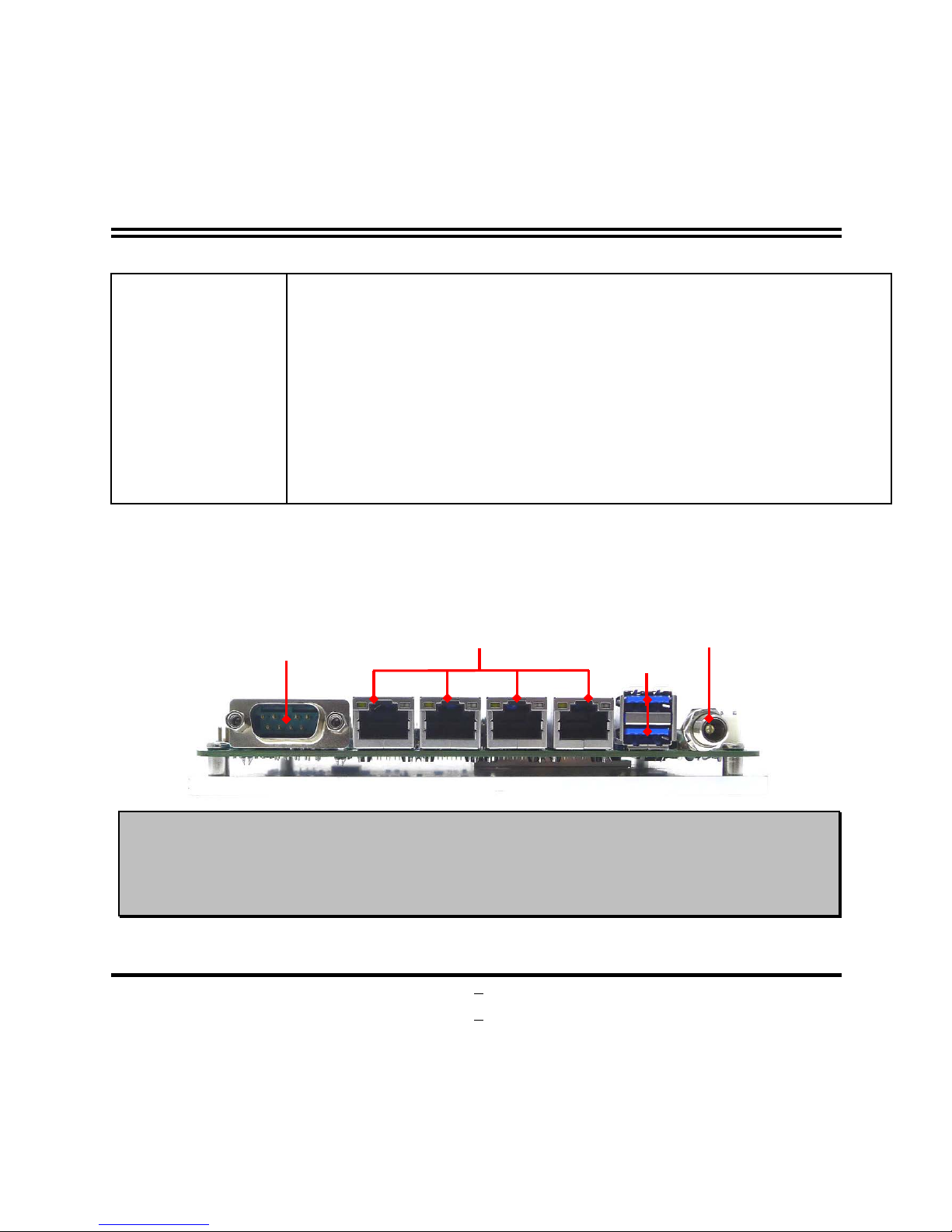
Rear IO Panel Diagram:
Warning!!
The board has a 12V DC-in power conne ctor (DCI N) in I /O back pane l and an int ernal ATX12V
(ATX2P) power connector. User can only connect one type of compatible power supply to o ne
of them to power the system.
RJ-45 LAN Ports
(LAN1/2/3/4)
COM1 Serial Port
USB 3.0 Ports
12V DC-in
Power Connector
4
Motherboard Internal Diagram-Front Side
Note: SIM card slot only work when c ompati bl e SIM card installed & 3G LAN card installed in MPE1 Mini-PCIE slot.
*SIM Card Sl ot
DDR4
SO-DIMM Slot
(SODIMM1)
Full-size Mini-PCIE Slot
(MPE1)
Half-size Mini-PCIE Slot
(MPE2)
Full-size Mini-SATA
Slot (MSATA)
HDMI Header
PS/2 Keyboard
& Mouse Header
Internal 12V DC-in
Power Connector
Speaker & PWRLED
Header
LANLED
Header
Front Panel
Header
CPUFAN Header
SATAIII Port
SATA HDD
Power Connector
USB 2.0 Header
SMBUS Header
USB 3.0 Ports
12V DC-in
Power Connector
(Lockable)
LAN1
RJ-45 LAN Port
LAN2
RJ-45 LAN Port
LAN3
RJ-45 LAN Port
LAN4
RJ-45 LAN Port
COM1 Port
GPIO Header
USB 2.0
Header
Serial Port
Header
5
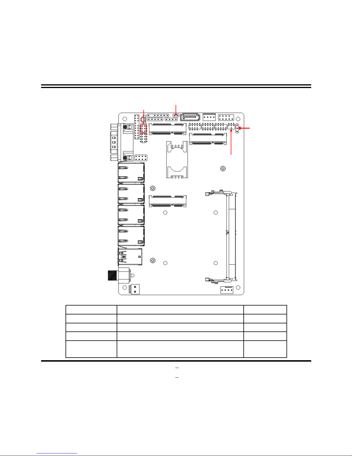
Jumper Position:
Jumper
Jumper
Name
Description
JPCOM2
COM2 Header Pin9 Function Select
4-Pin Block
AT_MODE
ATX Mode / AT Mode Select
3-Pin Block
COPEN
Case Open Message Display Function
2-Pin Block
JBAT_MERTC
Pin 1&2: Clear CMO S
Pin 3&4: Flash Override
6-Pin Block
JPCOM2
JBAT_ MERTC
AT_MODE
COPEN
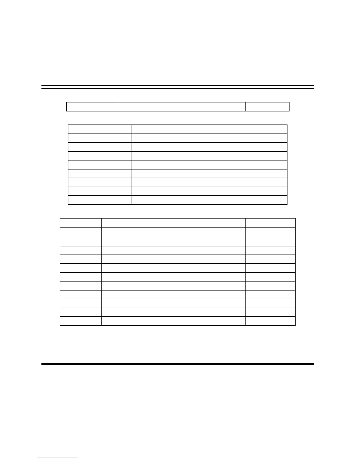
6
Pin 5&6: POK Override
Connectors
Connector
Name
DCIN
12V System DC–in Power Jack Connector
USB1
USB 3.0 Port Connector X2
LAN1/2/3/4
RJ-45 LAN Port Connector x 4
COM1
Serial Port Connector
ATX2P
Internal 12V System DC–in Power Connector
CPUFAN
CPU Fan Connector
SATA1
SATAIII Port Connector
STATPWR
SATA Power out Connector
Headers
Header
Name
Description
JW_FP
Front Panel Header
(PWR LED/ HD
D LED/Power Button /Reset)
9-pin Block
SPK-LED
Power LED & Speaker Header
8-pin Block
LAN_LED
LAN Activity LED Header
8-pin Block
COM2
Serial Port Header
9-pin Block
GPIO_CON
GPIO Header
10-pin Block
FP_USB1
USB 2.0 Header
9-pin Block
FP_USB2
USB 2.0 Header
4-pin Block
SMBUS
SMBUS Header
5-pin Block
PS2KBMS
PS/2 Keyboard & Mouse Header
6-pin Block
HDMI
HDMI Header
19-pin Block
7
Chapter 2
Hardware Installation
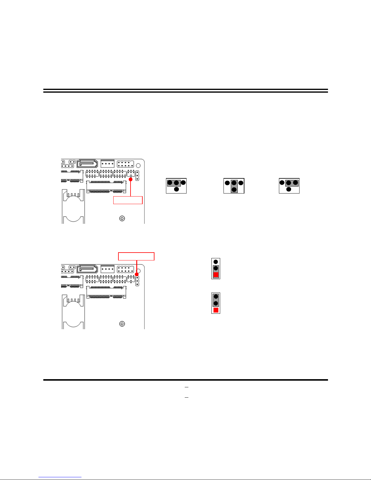
2-1 Jumper Setting
JPCOM2 (4-pin): COM2 Header Pin9 Function Select
JPCOM
2→COM
2 Header Pin-9
6 4 2
3
1
5
1
3 5
2
4
6
1
3
5
2
4
6
2-4 Closed
:
RING( Default)
;
3-4 Closed:
5V;
4-6 Closed:
12V.
AT_MODE (3-pin): ATX Mode/AT Mode Select
AT_MODE→ATX/AT Mode Select
3
1
1
3
1-2 Close: ATX ModSelected(Default);
2-3 Close: AT ModSelected.
*ATX Mode Selected: Press power button to power on after power input ready;
AT Mode Selected: Directly power on as power input ready.
JPCOM2
AT_MODE
8
COPEN (2-pin): Case Open Message Display Function Select
1-2 Open:
Normal (Default);
1
1-2 Closed:
Case Open.
1
Pin (1-2) Close: When C ase O pen func tion pi n short to GN D, the C ase O pen f unctio n
was detected. When Used, needs to enter BIOS and enable ‘Case Open Detect’
function. In this case if your case is removed, next time when you restart your
computer, a message will be displayed on screen to inform you of this.
Pin 1&2 of JBAT_MERTC (6-pin): Clear C MOS Setting
Pin 1&2 of JBAT→ Clear CMOS Setting
Pin 1
1-2
Closed
: Clear CMOS
.
1-2 Open:
Normal;
2
2
Pin 1
JBAT_MERTC
COPEN
9
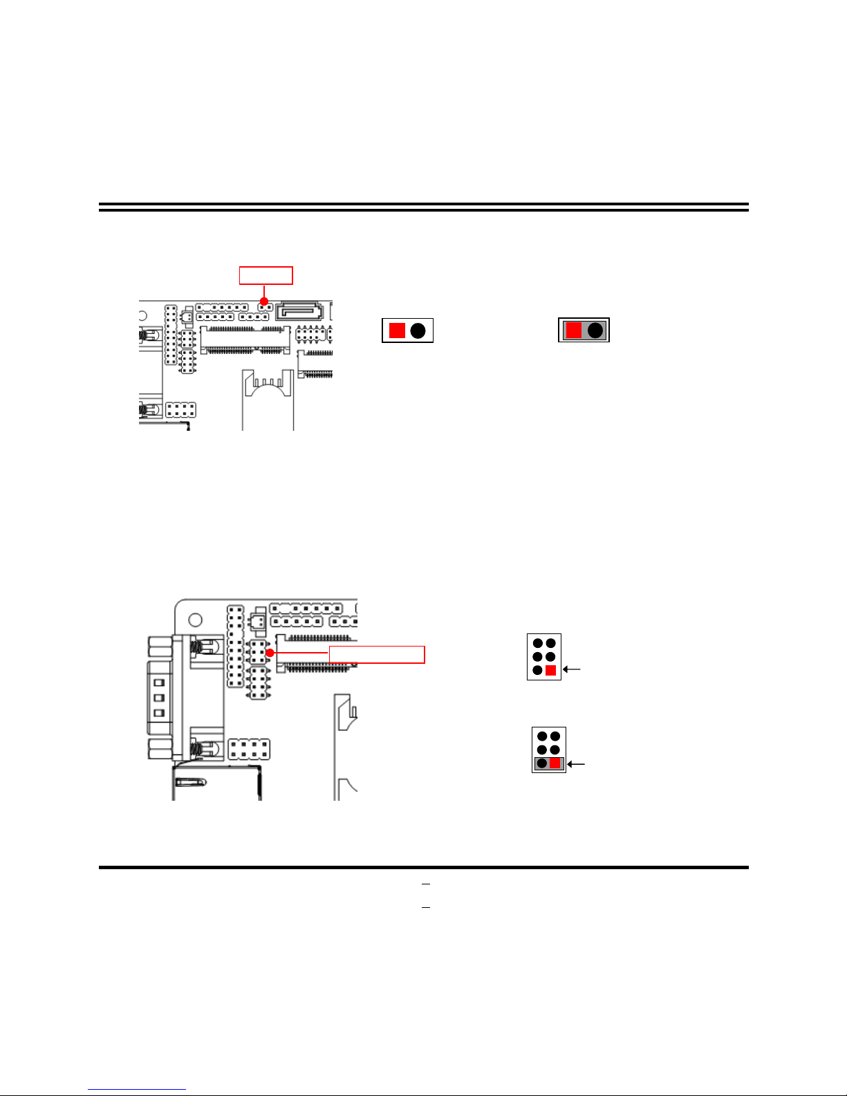
Pin 3&4 of JBAT_MERTC (6-pin): Flash Override Function Slect
Pin 3&4 of JBAT→ Flash Override
Pin 3
4
4
Pin 3
3-4 Open:Enable Security Measures
in the Flash Descriptor(Default);
3-4 Closed: Disable Security Measures
in the Flash Descriptor(Override).
Pin 5&6 of JBAT_MERTC (6-pin): POK Override Function Slect
Pin 5&6 of JBAT→ POK Override
Pin 5
6
6
Pin 5
5-6 Open:Normal;
5-6 Closed: POK Override.
JBAT_MERTC
JBAT_MERTC
 Loading...