

Page 1

NC7A Series User M anual
NO. G03-NC7A-F
Revision: 1.0
Release date: July 31, 2017
Trademark:
* Specifications and Informati on cont a ined in t his docu me nt ation are furnished for informatio n u se only, and are
subject to change at any time without notice, and should not be construed as a commitment by manufacturer.
Page 2

i
Environmental Pr otecti on Announcement
Do not dispose this electronic device into the trash while discarding. To minimize
pollution and ensure environment protection o f mother ear th, pl ease recycle.
Page 3

ii
ENVIRONMENTAL SAFETY INSTRUCTION ........................................................................... iii
USER’S NOTICE ....................................................................................................................... iv
MANUAL REVISION INFORMATION ....................................................................................... iv
ITEM CHECKLIST ..................................................................................................................... iv
CHAPTER 1 INTRODUCTION
1-1 PRODUCT FEATURES ............................................................................................... 1
1-2 SPECIFICATION ......................................................................................................... 2
1-3 MAIN BOARD DIAGRAM ........................................................................................... 3
CHAPTER 2 HARDWARE INSTALLATION
2-1 LOCATION OF INTERNAL JUMPER AND CONNECTOR ....................................... 5
2-2 INTERNAL JUMPER AND CONNECTOR SETTING ................................................. 6
2-2-1 CONNECTORS ............................................................................................. 10
2-2-2 HEADERS ..................................................................................................... 11
CHAPTER 3 INTRODUCING BIOS
3-1 ENTERING SETUP ..................................................................................................... 19
3-2 BIOS MENU SCREEN ................................................................................................ 20
3-3 FUNCTION KEYS ....................................................................................................... 20
3-4 GETTING HELP .......................................................................................................... 21
3-5 MEMU BARS ............................................................................................................... 21
3-6 MAIN MENU ................................................................................................................ 21
3-7 ADVANCED MENU ..................................................................................................... 23
3-8 CHIPSET MENU .......................................................................................................... 33
3-9 SECURITY MENU ....................................................................................................... 35
3-9 BOOT MENU ............................................................................................................... 36
3-11 SAVE & EXIT MENU ................................................................................................... 37
TABLE OF CONTENT
Page 4

iii
Environmental Safety Instruction
Avoid the dusty, humidity and temperature extremes. Do not place the product in
any area where it may become wet.
0 to 60 centigrade is th e suitabl e tem perat ure. (The figure c omes from the r eques t
of the main chipset)
Generally speaking, dramatic changes in temperature may lead to contact
malfunction and crackles due to constant thermal expansion and contraction from
the welding spots’ that connect components and PCB. Computer should go
through an adaptive phase before it boots when it is moved from a cold
environment to a warmer one to avoid condensation phenomenon. These water
drops attached on PCB or the surface of the components can bring about
phenomena as minor a s computer instabi lity resulted fr om corrosi on and oxi dation
from components and PCB or as major as short circuit that can burn the
components. Suggest starting the computer until the temperature goes up.
The increasing temperature of the capacitor may decrease the life of computer.
Using the close case may decrease the life of other device because the higher
temperature in the inner of the case.
Attention to the heat sink when you over-clocking. The higher temperature may
decrease the life of the device and burned the capacitor.
Page 5

iv
USER’S NOTICE
COPYRIGHT OF THIS MANUAL BELONGS TO THE MANUFACTURER. NO PART OF THIS MANUAL,
INCLUDING THE PRODUCTS AND SOFTW ARE DESCRIBED I N IT MAY BE REPRO DUCED, T RANSMITTED
OR TRANSLATED INTO ANY LANGUAGE IN ANY FORM OR BY ANY MEANS WITHOUT WRITTEN
PERMISSION OF THE MANUFACTURER.
THIS MANUAL CONTAINS ALL INFORMATION REQUIRED TO USE THIS MOTHER-BOARD SERIES AND WE
DO ASSURE THIS MANUAL MEETS USER’S REQUIREMENT BUT WILL CHANGE, CORRECT ANY TIME
WITHOUT NOTICE. MANUFACTURER PROVIDES THIS MANUAL “AS IS” WITHOUT WARRANTY OF ANY
KIND, AND WILL NOT BE LIABLE FOR ANY INDIRECT, SPECIAL, INCIDENTAL OR CONSEQUENTIAL
DAMAGES (INCLUDING DAMAGES FOR LOSS OF PROFIT, LOSS OF BUSINESS, LOSS OF USE OF DATA,
INTERRUPTION OF BUSINESS AND THE LIKE).
PRODUCTS AND CORPORATE NAMES APPEARING IN THIS MANUAL MAY OR MAY NOT BE
REGISTERED TRADEMARKS OR COPYRIGHTS OF THEIR RESPECTIVE COMPANIES, AND THEY ARE
USED ONLY FOR IDENTIFICATION OR EXPLANATION AND TO THE OWNER’S BENEFIT, WITHOUT
INTENT TO INFRINGE.
Manual Revision Information
Reversion Revision History Date
1.0 First Edition July 31, 2017
Item Checklist
Motherboard
DVD for motherboard utilities
User’s Manual
Cable(s)
I/O Back panel shield
Page 6

1
Chapter 1: Introduction
1-1 Product Features
Intel® Celeron™ J1900 (2.0 GHz) quad-core processor
Support DirectX 11 3D Graphics Acceleration
Onboard SAMSUNG 4G/1333MHz DDR3L Memory
Support up to 2 Displays, LVDS,EDP, VGA
1 x SATA3 6Gb/s Port
1 x MINI PCI-E Socket
1 x M.2 Socket (2242/2260/2280)
Dual Intel® Gig abi t LA N
4 x Serial Ports (COM1/2 RS232/422/485), 8-bit GPIO
2 x USB 3.0 Ports, 6 * USB 2.0 Ports, Watchdog Timer
9 ~ 28V DC-in or 4-pin Internal Power Connector
5.25” Form Factor (120mm * 200mm)
Page 7

2
1-2 Specification
Spec
Description
CPU
Intel® Celeron™ J1900 (2.0 GHz) quad-core processor
Memory
Onboard SAMSUNG 4G/1333MHz DDR3L up to 8GB
Expansion Slot
1* Full-size Mini PCIe slot
1* M.2 (2242/2260/2280)
1* SIM Card Holder
Storage
1* SATA III 6G/s Connector
LAN Chip
2* Intel® i211AT GbE
Support Fast Ethernet LAN function of providing
10/100/1000Mbps Ethernet data transfer rate
Audio Chip
Realtek ALC662 dual channel HD Audio Codec integrated
Audio driver and utility included
BIOS
AMI 64MB Flash ROM
Rear I/O
1 * VGA
2* RJ45, 10/100/1000 Mbps
2* USB3.0, 2* USB2.0 ports
2* RS232/422/485 ports with 5V/12V selectable header
1* DC-in, 1* Power Button
Internal I/O
2* USB 2.0 header
1* PS/2 header
1* LVDS, 1* eD P
2* RS-232 with 5V/12V selectable header
1* SATA III 6G/s Connector
1* Full-size Mini PCIe
1* M.2 (2242/2260/2280)
1* GPIO (4 in/4 out)
1* Chassis intrusion, 1* Audio Header, 1* SMBUS/I2C
1* AT_ATX Mode header
1* Support Expansion card(2* COM+2* USB2.0)
Page 8
3
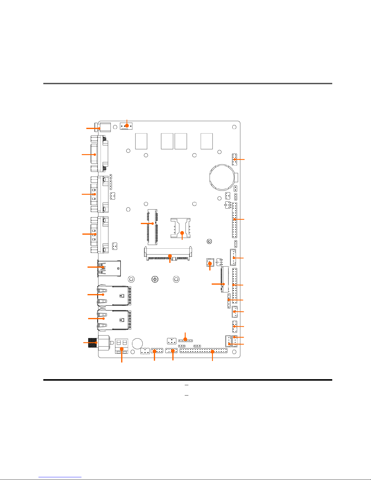
1-3 Main Board Diagram: Front
Power Button
VGA
USB3.0 Ports
COM1
COM2
Top:
RJ-45
LAN Port1
Middle/Bottom:
USB2.0 Port
Top:
RJ-45
LAN Port2
Middle/Bottom:
USB2.0 Port
DC-in
Connector
CPUFAN Header
Mini PCIe
Connector
SIM Card Socket
SATA3 Connector
JW_FP Header
EDP1 Header
INVERTER1 Header
JP3 Header
M.2 Connector
SPEAK_CON2 Header
F_USB1 Header
F_USB2Header
DCIN3 Connector
F_PH1 Connector
PS2_CON1 Header
COM3
COM4
LVDS1 Header
SMBUS Header
FP_AUDIO Header
Page 9
4
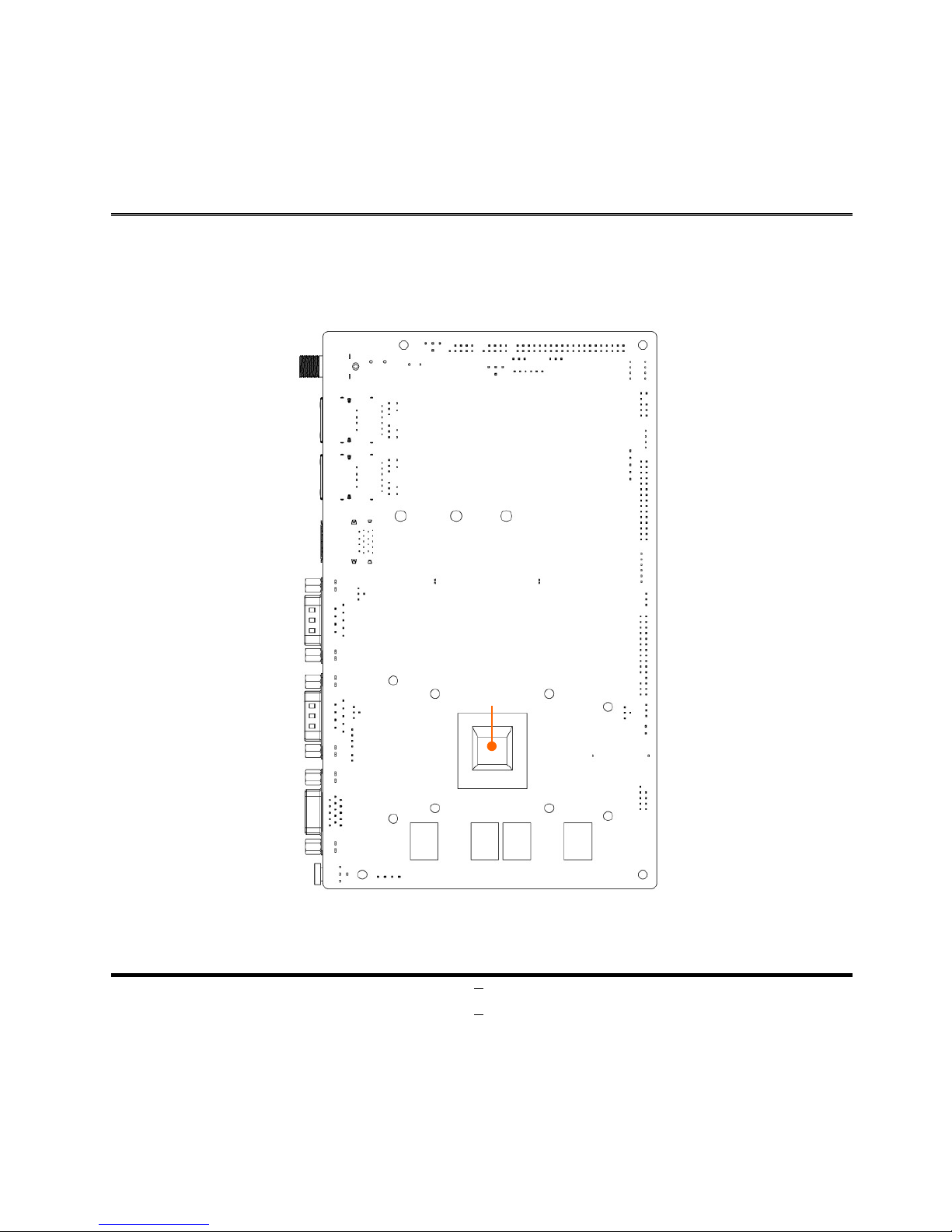
Main Board Diagram: Back
Intel CPU
Page 10
5
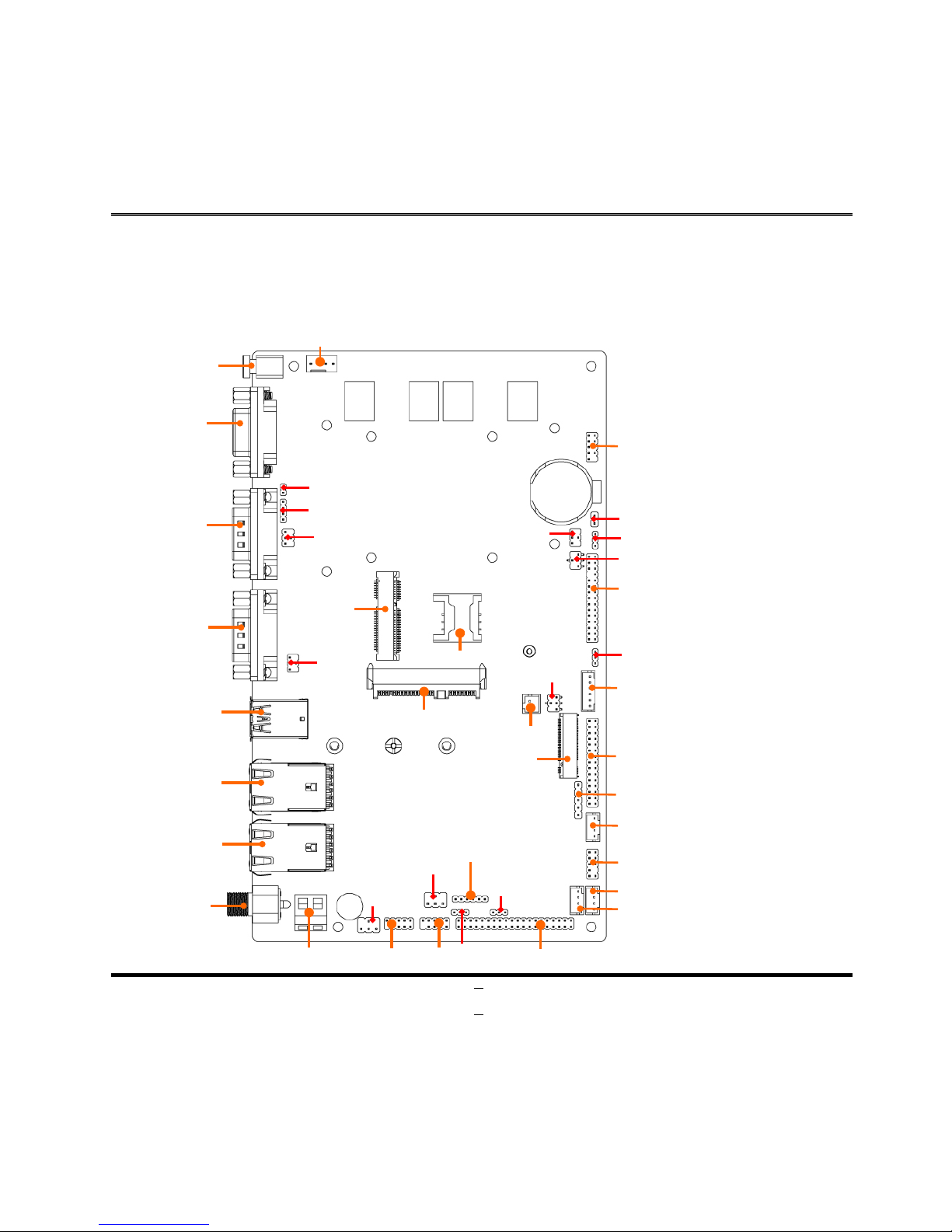
Chapter 2
Hardware Installation
2-1 Location of Internal Jumper and Connector
Power Button
VGA
USB3.0 Ports
COM1
COM2
Top:
RJ-45
LAN Port1
Middle/Bottom:
USB2.0 Port
Top:
RJ-45
LAN Port2
Middle/Bottom:
USB2.0 Port
DC-in
Connector
CPUFAN Header
Mini PCIe
Connector
SIM Card Socket
SATA3 Connector
JW_FP Header
EDP1 Header
INVERTER1 Header
JP3 Header
M.2 Connector
SPEAK_CON2 Header
F_USB1 Header
F_USB2 Header
DCIN3 Connector
COPEN
JP1
JP2
JBAT1
JPLED
JPLCD
AT_MODE
JPCOM4
JP4
JPCOM3
JPCOM2
JPCOM1
I2C
JP5
LVDS1 Header
SMBUS Header
FP_AUDIO Header
F_PH1 Connector
PS2_CON1 Header
COM3
COM4
Page 11
6
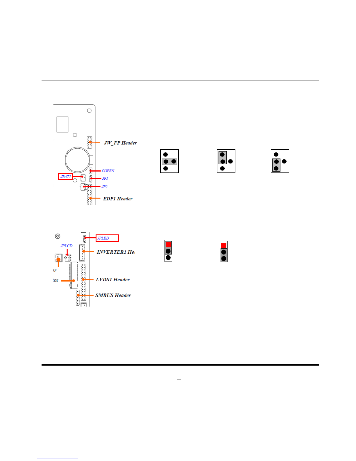
2-2 Internal Jumper and Connector Setting
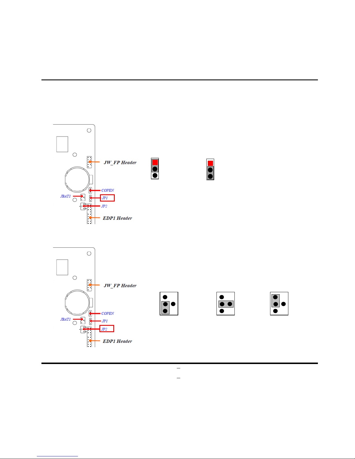
(1) JP1 (3-pin): eDP Backlight VCC 5V /12V Select
1
1-2 Closed:
5V (Default);
3
1
3
2-
3 Closed:
12
V.
(2) JP2 (4-pin): eDP LCD VCC 3.3V / 5V /12V Select
4-6 Closed:
12V.
3-4 Closed:
5V;
2-4 Closed:
3.3V (Default);
3
6
4
2
3
6
4
2
3
6
4
2
Page 12
7
(3) JBAT1 (4-pin): Clear CMOS Setting
4-6 Closed:
RTC_RST.
2-4 Closed:
CLEAR CMOS;
3-4 Closed:
(Default);
3
2
4
6
3
2
4
6
3
2
4
6
(4) JPLED (3-pin): LVDS Backlight VCC 5V / 12V Select
1
1-2 Closed
:
5V (Default);
3
1
3
2-3 Closed:
12V.
Page 13
8
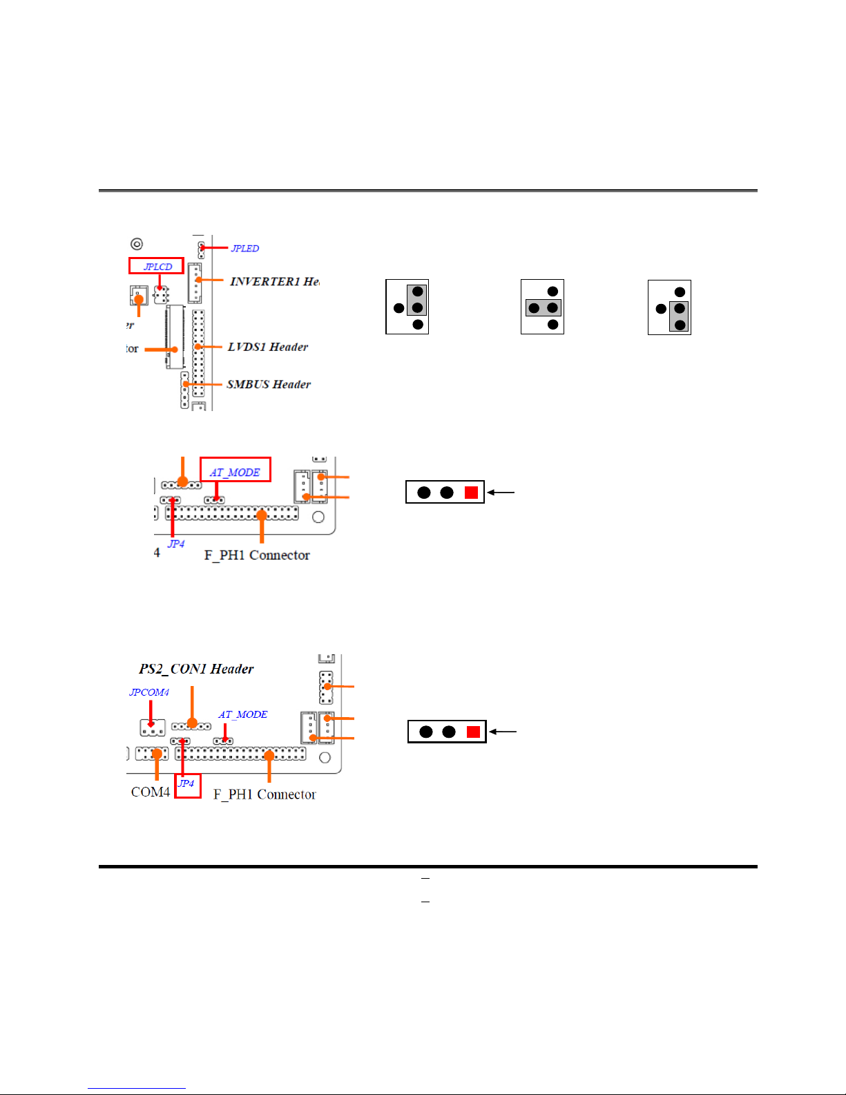
(5) JPLCD (4-pin): LVDS LCD VCC 3.3V / 5V /12V Select
4-6 Closed:
12V.
3-4 Closed:
5V;
2-4 Closed:
3.3V
(Default);
3
2
4
6
3
2
4
6
3
2
4
6
(6) AT_Mode (3-pin): AT/ATX Mode Function Select
AT Mode.
Pin1
2-3 Closed:
ATX Mode (default);
1-2 Closed:
*ATX Mode Selected: Press power button to power on after power input ready;
AT Mode Selected: Directly power on as power input ready.
(7) JP4 (3-pin): PS2 5V SB / VCC Select
VCC.
Pin1
2-3 Closed:
5VSB (default);
1-2 Closed:
Page 14

9
(8) JPCOM1/2/3/4 (4-pin): COM1/COM2/COM3/COM4 5V /12V Select
4-6 Closed:
12V.
3-4 Closed:
5V;
2-4 Closed:
RING (Default);
3 2 4 6 3 2 4 6 3 2 4
6
4-6 C
losed:
12V.
3-4 Closed:
5V;
2-4 Closed:
RING (Default);
3
2
4
6
3
2
4
6
3
2
4
6
Page 15

10
2-2-1 Connectors
(1) Rear I/O Connectors
Icon Name Function
Power Button
Press to turn on/off the system.
VGA Port
T
o connect display device that support VGA
specification.
COM Port
Mainly for user to connect external MODEM
or other
devices that supports Serial Communications Interface.
USB 3.0 Port
To
connect USB keyboard, mouse or other devices
compatible with USB specification.
USB 3.0 ports
supports up to 5Gbps data transfer rate.
RJ-45 LAN Port
This connector is s tandard RJ-45 LAN j ack
for Network
connection.
USB 2.0 Port
To
connect USB keyboard, mouse or other devices
compatible with USB specification.
DC-in Power Jack
Connector
For user to connect compatible power adapter to provide
power supply for the system.
COM1
Power Button
USB 3.0 Port
RJ-45
LAN2 Port
RJ-45
LAN1 Port
COM2
USB 2.0 Port
VGA
DC-in
Page 16

11
2-2-2 Headers
(1) CPUFAN (4-pin): CPUFAN Header
(2) JW_FP (9-pin): Front Panel Header
VCC
HLED-
GND
FP_RST-
VSB_LED
PWRLED
GND
FP_SPSW
HLED+
PIN 1
2
Page 17

12
(3) COPEN (2-PIN): Case Open Message Display Function
1
2
COPEN-
GND
Pin 1-2 Close: When Case open function pin short to GND, the C ase open function
was detected. When Used, needs to enter BIOS and enable ‘Case Open Detect’
function. In this case if your case is removed, next time when you restart your
computer, a message will be displayed on screen to inform you of this.
(4) EDP1 (30-pin): eDP Header
Pin 29
Pin30
Pin1
Pin2
Page 18

13
Pin NO.
Pin Define
Pin NO.
Pin Define
Pin 1
BKLT_PW
Pin 2
EDP_INVCC
Pin 3
BKLT_PW
Pin 4
GND
Pin 5
GND
Pin 6
NC
Pin 7
NC
Pin 8
NC
Pin 9
EDP_LCD_VCC
Pin 10
NC
Pin 11
EDP_LCD_VCC
Pin 12
EDP_BKLTCTL
Pin 13
GND
Pin 14
GND
Pin 15
EDP_BKLTEN
Pin 16
EDP_AUXP_C
Pin 17
EDP_HPD
Pin 18
EDP_AUXN_C
Pin 19
GND
Pin 20
GND
Pin 21
EDP_LAN+3
Pin 22
EDP_LANE-3
Pin 23
EDP_LAN+2
Pin 24
EDP_LANE-2
Pin 25
GND
Pin 26
GND
Pin 27
EDP_LAN+1
Pin 28
EDP_LANE-1
Pin 29
EDP_LAN+0
Pin 30
EDP_LANE-0
(5) INVERTER1 (6-Pin): LVDS1 Inverter Header
Page 19

14
(6) JP3 (2-Pin): Brightness Setting Header
BRTNSS_UP
BRTNSS_DN
(7) LVDS1 (30-Pin): 24-bit dual channel LVDS Header
Pin 2
Pin 1
Pin NO.
Pin Define
Pin NO.
Pin Define
Pin 1
LVD_VCC
Pin 2
LVD_VCC
Pin 3
LVD_VCC
Pin 4
LVDS_PRSNT#
Pin 5
GND
Pin 6
GND
Pin 7
LVDSA_DATAN0
Pin 8
LVDSA_DATAP0
Page 20

15
Pin 9
LVDSA_DATAN1
Pin 10
LVDSA_DATAP1
Pin 11
LVDSA_DATAN2
Pin 12
LVDSA_DATAP2
Pin 13
GND
Pin 14
GND
Pin 15
LVDSA_CLKN
Pin 16
LVDSA_CLKP
Pin 17
LVDSA_DATAN3
Pin 18
LVDSA_DATAP3
Pin 19
LVDSB_DATAN0
Pin 20
LVDSB_DATAP0
Pin 21
LVDSB_DATAN1
Pin 22
LVDSB_DATAP1
Pin 23
LVDSB_DATAN2
Pin 24
LVDSB_DATAP2
Pin 25
GND
Pin 26
GND
Pin 27
LVDSB_CLKN
Pin 28
LVDSB_CLKP
Pin 29
LVDSB_DATAN3
Pin 30
LVDSB_DATAP3
*Note: LVDS is optional by customized order.
(8) SMBUS (5-pin): SMBUS Function Header
Pin 1
SCL
SDA
SMBALERT-
GND
VCC3
(9) SPEAK_CON2 (4-pin): Speaker Header
Page 21

16
(10) FP_AUDIO (9-pin): Line-Out, MIC-In Header
This header connects to Front Panel Line-out, MIC-In connector with cable.
Pin 1
2
MIC2-L
MIC2-R
LINE2-R
LINE2-L
GND
F_AUDIO_DET-
MIC2_RTU
NC
LINE2_RTU
SENSE B
(11) F_USB1/2 (4-pin): USB 2.0 Port Header
(12) F_PH1 (40-pin): COM Port Expansion Header & GPIO Header
Pin 1
2
Page 22

17
Pin NO.
Pin Define
Pin NO.
Pin Define
Pin 1
VCC
Pin 2
VCC
Pin 3
GL850_USBN3_A
Pin 4
GL850_USBN4_A
Pin 5
GL850_USBP3_A
Pin 6
GL850_USBP4_A
Pin 7
GND
Pin 8
GND
Pin 9
GND
Pin 10
NC
Pin 11
DCD5-
Pin 12
DSR5-
Pin 13
SIN5
Pin 14
RTS5-
Pin 15
SOUT5
Pin 16
CTS5-
Pin 17
DTR5-
Pin 18
RI5-
Pin 19
GND
Pin 20
NC
Pin 21
DCD6-
Pin 22
DSR6-
Pin 23
SIN6
Pin 24
RTS6-
Pin 25
SOUT6
Pin 26
CTS6-
Pin 27
DTR6-
Pin 28
RI6-
Pin 29
GND
Pin 30
NC
Pin 31
SIO_GPIO80
Pin 32
SIO_GPIO81
Pin 33
SIO_GPIO82
Pin 34
SIO_GPIO83
Pin 35
SIO_GPIO84
Pin 36
SIO_GPIO85
Pin 37
SIO_GPIO86
Pin 38
SIO_GPIO87
Pin 39
GND
Pin 40
VCC
(13) PS2_CON1 (6-pin): Keyboard / Mouse Connector Header
MCL
PS2VCC
MDA
KBDAT
GND
KB CLK
PIN 1
Page 23

18
(14) COM3/4 (9-pin): COM3 / COM4 Header
Pin 1
2
MDSR-
MRTS-
MCTSMDCD-
MSIN-
MSO-
MDTR-
GND
COM_MRI-
(15) DCIN3 (2-pin block): DC input Header
Page 24

19
Chapter 3
Introducing BIOS
Notice! The BIOS options in this manual are for reference only. Different
configurations may lead to difference in BIOS screen and BIOS screens
in manuals are usually the first BIOS version when the board is released
and may be different from your purchased motherboard. Users are
welcome to download the latest BIOS version form our official website.
The BIOS is a program located on a Flash Memory on the motherboard. This program
is a bridge between motherboard and operating system. When you start the computer,
the BIOS program will gain control. The BIOS first operates an auto-diagnostic tes t called
POST (power on sel f t est) for all the neces sar y hardw are, i t detects the enti re hardw are
device and configures the parameters of the hardware synchronization. Only when
these tasks are co mpleted done it gives up control of th e computer to operating system
(OS). Since the BIOS is the only channel for hardware and software to communicate, it
is the key factor for system stability, and in ensuring that your system performance as
its best.
3-1 Entering Setup
Power on the computer and by pressing <Del> immediately allows you to enter Setup.
If the message disappears before your respond and you still wish to enter Setup,
restart the system to try again by turning it OFF then ON or pressing the “RESET”
button on the system case. You may also restart by simultaneously pressing <Ctrl>,
<Alt> and <Delete> keys. If you do not press the keys at the correct time and the
system does not boot, an error message will be displayed and you will again be asked
to
Press <Del> to enter Setup
Page 25

20
3-2 BIOS Menu Screen
The following diagram show a general BIOS menu screen:
BIOS Menu Screen
3-3 Function Keys
In the above BIOS Setup main menu of, you can see several options. We will explain
these options step by step in the following pages of this chapter, but let us first see a
short description of the function keys you may use here:
Press←→ (left, right) to select screen;
Press ↑↓ (up, dow n) to cho ose, i n the mai n m enu, th e optio n you w a nt t o con firm or
to modify.
Press <Enter> to select.
Menu
Bar
Menu Items
Current Setting Value
Function Keys
General Help Items
Page 26

21
Press <+>/<–> keys when you want to modify the BIOS parameters for the active
option.
[F1]: General help.
[F2]: Previous values.
[F3]: Optimized defaults.
[F4]: Save & Exit.
Press <Esc> to quit the BIOS Setup.
3-4 Getti ng H elp
Main Menu
The on-line description of the highlighted setup function is displayed at the top right
corner the screen.
Status Page Setup Menu/Option Page Setup Menu
Press [F1] to pop up a small help window that describes the appropriate keys to use
and the possible selections for the highlighted item. To exit the Help Window, press
<Esc>.
3-5 Menu Bars
There are six menu bars on top of BIOS screen:
Main
To change system basic configuration
Advanced
To change system advanced configuration
Chipset
To change chipset configuration
Security
Password settings
Boot
To change boot settings
Save & Exit
Save setting, loading and exit options.
User can press th e rig ht or lef t arrow k ey on t he key boar d to sw itch fr om men u bar . Th e
selected one is highlighted.
3-6 Main Menu
Main menu scre en inc l udes some basic system information. Highlight the item and then
use the <+> or <-> and numerical keyboard keys to select the value you want in each
item.
Page 27

22
System Date
Set the date. Please use [Tab] to switch between date elements.
System Time
Set the time. Please use [Tab] to switch between time elements.
Page 28

23
3-7 Advanced Menu
OS Selection
Use this item to select OS.
The optional settings are: [Windows 8.X]; [Linux/Android]; [Windows 7].
Trusted Computing
Press [Enter] to make setti ng s for the fol l owing sub-item:
Security Device Support
Use this item to enable or disable BIOS support for security device. OS will not
show Security Device. TCG EFI protocol and INT1A interface will not be available.
The optional settings: [Disabled]; [Enabled].
When set as [Enabled], the following sub-items shall appear:
TPM State
Use this item to enable or disable Security Device. NOTE: computer will reboot
during restart in order to change state of the Device.
The optional settings: [Disabled]; [Enabled].
Page 29

24
ACPI Settings
Press [Enter] to make setti ng s for the fol l owing sub-item:
ACPI Sleep State
Use this item to select ACPI sleep state the system will enter when the suspend
button is pressed.
The optional settings are: [Suspend Disabled]; [S3 only (Suspend to RAM) ].
► Super I/O Configuration
Press [Enter] to make setti ng s for the fol l owing sub-items:
► Serial Port 1/2 Configuration
Press [Enter] to make setting s for the f oll owing items:
Serial Port
Use this item to enable or disable serial port (COM).
The optional settings are: [Disabled]; [Enabled].
Change Settings
Use this item to select an optimal setting for super IO device.
The optional settings are: [Auto]; [IO=3F8h; IRQ=4;]; [IO=2F8h; IRQ=3;];
[IO=3E8h; IRQ=4;]; [IO=2E8h; IRQ=3;].
Transmission Mode Select
Use this item to select transmission mode.
The optional settings are: [RS422]; [RS232]; [RS 485].
Serial Port FIFO Mode
Use this item to select an optimal setting for FIFO Mode.
The optional settings are: [16-Byte FIFO]; [32-Byte FIFO]; [64-Byte FIFO];
[128Byte FIFO].
► Serial Port 3/4/5/6 Configuration
Press [Enter] to make settings for the f oll owing items:
Serial Port
Use this item to enable or disable serial port (COM).
The optional settings are: [Disabled]; [Enabled].
Change Settings
Use this item to select an optimal setting for super IO device.
The optional settings are: [Auto]; [IO=3F8h; IRQ=10;]; [IO=2F8h; IRQ=10;];
Page 30

25
[IO=3E8h; IRQ=10;]; [IO=2E8h; IRQ=10;]; [IO=2F0h; IRQ=10;]; [IO=2E0h;
IRQ=10;].
Serial Port FIFO Mode
U se this item to select an optimal setting for FIFO Mode.
The optional settings are: [16-Byte FIFO]; [32-Byte FIFO]; [64-Byte FIFO];
[128Byte FIFO].
OS Select for Serial Port
Serial port supports for Windows or Linux. The optional settings are: [Windows];
[LINUX].
ERP Support
Use this item to disable or enable ERP to active all wake-up functions.
The optional settings are: [Disabled]; [Enabled].
Case Open Detect
Use this item to disable or enabl e c ase open func tio ns an d s how me ssag e in P OST .
The optional settings are: [Disabled]; [Enabled].
PS2 KB/MS Connect
Use this item to set PS2 Connect Primary Devices.
The optional settings are: [Keyboard First]; [Mouse First].
WatchDog Reset Timer
This item support WDT reset function.
The optional settings: [Disabled]; [Enabled].
Use this item to en abl e or di sabl e WatchDog Timer Contr ol . When set as [Enabled ] ,
the following sub-items shall appear:
WatchDog Reset Timer Value
User can set a value in the range of [10] to [255] seconds or in the ra nge of [1] to
[255] minutes.
WatchDog Reset Timer Unit
The optional settings are: [Sec.]; [Min.].
WatchDog Wake-up Timer
Support WDT Wake-up.
The optional settings: [Disabled]; [Enabled]. When set as [Enabled], the following
sub-items shall appear:
WatchDog Wake-up Timer Value
Page 31

26
User can set a value in the range of [10] to [4095] seconds when‘WatchDog
Wake-up Timer Unit’ set as [Sec.], or in the range of [1] to [4095] minutes when
‘WatchDog Wake-up Timer Unit’ set as [Min.].
WatchDog Wake-up Timer Unit
The optional settings are: [Sec.]; [Min.].
Serial Port Console Redirection
COM1
Console Redirection
The optional settings: [Disabled]; [Enabled]. When set as [Enabled], the following
sub-items shall appear:
Console Redirection Settings
The settings specify how the host computer and the remote computer (which the
user is using) will exchange data. Both computers should have the same or
compatible settings.
Press [Enter] to make settings for the f oll owing items:
Terminal Type
The optional settings: [VT100]; [VT100+]; [VT-UTF8]; [ANSI].
Emulation: VT100: ASCII char set; VT100+: Extends VT100 to support color,
function keys, etc.; VT-UTF8: Uses UTF8 encoding to map Unicode chars onto 1
or more bytes; ANSI: Extended ASCII char set.
Bits per second
Use this item to select serial port transmission speed. The speed must be
matched on the other side. Long or noisy lines may require lower speeds.
The optional settings: [9600]; [19200]; [38400]; [57600]; [115200].
Data Bits
The optional settings: [7]; [8].
Parity
A parity bit can be sent with the data bits to detect some transmission errors.
The optional settings: [None]; [Even]; [Odd]; [Mark]; [Space].
Even: parity bit is 0 if the num of 1’s in the data bits is odd; Mark: parity bit is
always 1; Space: Parity bit is always 0; Mark and Space Parity do not allow for
error detection.
Stop Bits
Page 32

27
Stop bits indicate the end of a serial data packet. (A start bit indicates the
beginning). The standard settings is 1 stop bit. Communication with slow devices
may require more than 1 stop bit.
The optional settings: [1]; [2].
Flow Control
Flow control can pr event dat a loss fro m buffer over flow. When sending dat a, if the
receiving buffers are full, a “stop” signal can be sent to stop the data flow. Onc e
the buffers are empty, a “start” signal can be sent to re-start the flow. Hardware
flow control uses two wires to send start/stop signals.
The optional settings: [None]; [Hardware RTS/CTS].
VT-UTF8 Combo Key Support
Use this item to enable VT-UTF8 Combination Key Support for ANSI/VT100
terminals.
The optional settings: [Disabled]; [Enabled].
Recorder Mode
With this mode enable only text will be sent. This is to capture Terminal data.
The optional settings: [Disabled]; [Enabled].
Resolution 100x31
Use this item to enable or disable extended terminal resolution.
The optional settings: [Disabled]; [Enabled].
Legacy OS Redirection Resolution
On Legacy OS, the Number of Rows and Columns supported redirection.
The optional settings: [80x24]; [80x25].
Putty Ke yPad
Use this item to select FunctionKey and KeyPad on Putty.
The optional settings: [VT100]; [LINUX]; [XTERMR6]; [SCO]; [ESCN]; [VT400].
Redirection After BIOS POST
The settings specify if BootLoader is selected then Legacy console redirection is
disabled before booting to Legacy OS. Default value is Always Enable wich
means Legacy Console Redirection is enabled for Legacy OS.
The optional settings: [Always Enable]; [BootLoader].
Console Redirection
The optional settings: [Disabled]; [Enabled]. When set a s [Enabled], the following
sub-items shall appear:
Page 33

28
Console Redirection Settings
The settings specify how the host computer and the remote computer (which the
user is using) will exchange data. Both computers should have the same or
compatible settings.
Press [Enter] to make settings for the f oll owing items:
Terminal Type
The optional settings: [VT100]; [VT100+]; [VT-UTF8]; [ANSI].
Emulation: VT100: ASCII char set; VT100+: Extends VT100 to support color,
function keys, etc.; VT-UTF8: Uses UTF8 encoding to map Unicode chars onto 1
or more bytes; ANSI: Extended ASCII char set.
Bits per second
Use this item to select serial port transmission speed. The speed must be
matched on the other side. Long or noisy lines may require lower speeds.
The optional settings: [9600]; [19200]; [57600]; [115200].
Flow Control
Flow control can pr event dat a loss fro m buffer over flow. When sending dat a, if the
receiving buffers are full, a “stop” signal can be sent to stop the data flow. Once
the buffers are empty, a “start” signal can be sent to re-start the flow. Hardware
flow control uses two wires to send start/stop signals.
The optional settings: [None]; [Hardware RTS/CTS]; [Software Xon/Xoff].
PC Health Status
Press [Enter] to view current hardware health status, set shutdown temperature, or
make further settings in ‘SmartFan Configuration’.
SmartFan Configuration
Press [Enter] to make setti ng s for SmartFAN Configuration:
CPUFAN Type
The optional settings are: [4-Pin]; [3-Pin].
CPUFAN Smart Mode
The optional settings are: [Disabled]; [Enabled].
When set as [Enabled], the following sub-items shall appear:
CPUFAN Full-Speed Temperature
Use this item to set CPUFAN full speed temperature. Fan will run at full speed
when above the pre-set temperature.
Page 34

29
CPUFAN Full-Speed Duty
Use this item to set CPUFAN full speed duty. Fan will run at full speed when
above the pre-set duty.
CPUFAN Idle-Speed Temperature
Use this item to set CPUFAN idle speed temperature. Fan will run at idle speed
when below the pre-set temperature.
CPUFAN Idle-Speed Duty
Use this item to set CPUFAN idle speed duty. Fan will run at idle speed when
below the pre-set duty.
Shutdown Temperature
Use this item to select system shutdown temperature.
The optional settings are: [Disabled]; [70°C/156°F]; [75°C/164°F]; [80°C/172°F];
[85°C/180°F]; [90°C/188°F].
CPU Configuration
Press [Enter] to view current CPU configuration and make settings for the following
sub-items:
Limit CPUID Maximum
The optional settings: [Disabled]; [Enabled].
This item should be set as [Disabled] for Windows XP.
Execute Disable Bit
The optional settings: [Disabled]; [Enabled].
Hardware Prefetcher
The optional settings are: [Disabled]; [Enabled].
Use this item to enable the Mid Level Cache (L2) streamer prefetcher.
Adjacent Cache Line Prefetch
The optional settings are: [Disabled]; [Enabled].
Use this item to enable Mid Level Cache (L2) prefetching of adjacent cache lines.
CPU C State Report
Use this item to enable or disable CPU C state report to OS.
The optional settings: [Disabled]; [Enabled].
When set as [Enabled], user can see Enhanced C state:
Enhanced C state
Use this item to enable or disable CPU Cstate.
Page 35

30
The optional settings: [Disabled]; [Enabled].
Max CPU C-State
This item controls Max C-state that the processor will support.
The optional settings: [C7]; [C6]; [C1].
S0ix
Use this item to enable or disable CPU S0ix state.
The optional settings: [Disabled]; [Enabled].
SATA Configuration
Press [Enter] to make setti ng s for the fol l owing sub-items:
SATA Controller
The optional settings are: [Enabled]; [Disabled].
When user set it as [Enabled], the following items will show up for user to make
further settings:
SATA Speed Support
The optional settings are: [Gen1]; [Gen2].
SATA Mode Selection
The optional settings are: [IDE]; [AHCI].
SATAPort
The optional settings are: [Enabled]; [Disabled].
M.2
The optional settings are: [Enabled]; [Disabled].
Network Stack Configuration
Press [Enter] to go to ‘Network Stack’ screen to enable or disable UEFI Network
Stack.
Network Stack
The optional settings are: [Enabled]; [Disabled].
When set as [Enabled], the following sub-items shall appear:
Ipv4 PXE Support
The optional settings are: [Disabled]; [Enabled].
Use this item to enable Ipv4 PXE Boot Support. When set as [Disabled], Ipv4 boot
optional will not be created.
Ipv6 PXE Support
The optional settings are: [Disabled]; [Enabled].
Page 36

31
Use this item to enable Ipv6 PXE Boot Support. When set as [Disabled], Ipv6 boot
optional will not be created.
PXE Boot Wait Time
Use this item to set wait time to press [ESC] key to abort the PXE boot.
CSM Configuration
Boot Option Filter
This option controls Legacy/UEFI ROMs priority.
The optional settings are: [UEFI and Leg ac y ]; [Legacy only]; [UEFI only].
Network
This item controls the execution of UEFI and Legacy PXE OpROM.
The optional settings are: [Do Not Launch]; [UEFI only]; [Legacy only].
Storage
This option controls the execution of UEFI and Legacy Storage OpROM.
The optional settings are: [Do Not Launch]; [UEFI only]; [Legacy only].
Other PCI Devices
This item determines OpROM execution policy for devices other than Network,
storage or video.
The optional settings are: [UEFI First]; [Legac y Only].
Wakeup Function Settings
Press [Enter] to make setti ng s for the fol l owing sub-items:
Wake-up System with Fixed Time
Use this item to enable or disable system wake-up by RTC on alarm event.
The optional settings: [Disabled]; [Enabled].
When set as [Enabled], system will wake on the Hour/Minute/Second specified.
Wake-up System with Dynamic Time
Use this item to enable or disable system wake-up by RTC on alarm.
The optional settings: [Disabled]; [Enabled].
When set as [Enabled], system will wake on the (current time) + (Increase
minute(s)). The range is from [1] to [60] minute(s). .
PS2 KB/MS Wake-Up from S3-S5
PS2 KB/MS Wake-up is affected by ERP function in S4-S5. Please disable ERP
before activating this function in S4-S5.
The optional settings: [Disabled]; [Enabled].
Page 37

32
USB1 Wake-up from S3
Use this item to enable or disable USB wake-up. It is affected by ERP function in
S4. Please disable ERP before activating this function in S4.
The optional settings: [Disabled]; [Enabled].
USB Configuration
Legacy USB Support
The optional settings are: [Enabled]; [Disabled]; [Auto].
[Enabled]: To enable legacy USB support.
[Disabled]: To keep USB devices available only for EFI specification,
[Auto]: To disable legacy support if no USB devices are connected.
XHCI Hand-off
This is a workaround for O Ses without XHCI hand-of f support. The X HCI ownership
change should be claimed by XHCI driver.
The optional settings are: [Enabled]; [Disabled].
EHCI Hand-off
This is a workaround for O Ses without EHCI hand-of f support. The EH CI owner ship
change should be claimed by EHCI driver.
The optional settings are: [Disabled]; [Enabled].
USB Mass Storage Driver Support
The optional settings are: [Disabled]; [Enabled].
USB Transfer time-out
Use this item to set the time-out value for control, bulk, and interrupt transfers.
The optional settings are: [1 sec]; [5 sec]; [10 sec]; [20 sec].
Device reset time-out
Use this item to set USB mass storage device start unit command time-out.
The optional settings are: [10 sec]; [20 sec]; [30 sec]; [40 sec].
Device power-up delay
Use this item to set maximum time the device will take before it properly reports
itself to the host c ontr oller . ‘Aut o’ us es d efaul t v al ue: for a ro ot por t it i s 10 0 ms, for a
hub port the delay is taken from hub descr i pt or.
The optional settings: [Auto]; [Manual].
Select [Manual] you can set value for the following sub-item: ‘Device Power-up
Delay in Seconds’.
Device Power-up Delay in Seconds
Page 38

33
The delay range is from [1] to [40] seconds, in one second increments.
3-8 Chipset Menu
North Bridge
Press [Enter] to view current using memory information and make settings for the
following sub-items:
PAVC
Use this item to enable or disable Protected Audio Video Control.
The optional settings are: [Disabled]; [LITE Mode]; [SERPENT Mode].
DVMT Pre-Allocated
Use this item to select DVMT 5.0 pre-allocated (fixed) graphics memory size used
by the internal graphics device.
The optional settings are: [64M]; [96M]; [128M]; [160M]; [192M]; [224M]; [256M];
[288M]; [320M]; [352M]; [384M]; [416M]; [448M]; [480M]; [512M].
DVMT Total Gfx Mem
Use this item to select DVMT 5.0 total graphics memory size used by the internal
graphics device.
The optional settings are: [128M]; [256M]; [MAX].
Aperture Size
Page 39

34
The optional settings are: [128M]; [256M]; [512MB].
GTT Size
The optional settings are: [1M]; [2M].
Primary IGFX Boot Display
Use this item to select the video device which will be activated during POST. This
has no effect if external graphics present. Secondary boot display selection will
appear based on your selection. VGA modes will be supported only on primary
display.
The optional settings are: [VBIOS Default]; [CRT].
Active LFP
The optional settings are: [Disable]; [LVDS]; [eDP].
When set as [LVDS], user can make settings in ‘LCD Panel Type’.
The optional settings are: [800x600 24-bit 1ch]; [800x600 18-bit 1ch]; [1024x600
18-bit 1ch]; [1024x768 24-bit 1ch]; [1024x768 18-bit 1ch]; [800x480 18-bit 1ch];
[1366x768 18-bit 1ch]; [1440x900 18-bit 2ch]; [1366x768 24-bit 1ch]; [1440x900
24-bit 2ch]; [1280x1024 24-bit 2ch]; [1280x800 18-bit 1ch]; [1280x800 24-bit 1ch];
[1680x1050 24-bit 2ch]; [1280x768 24-bit 1ch]; [1920x1080 24-bit 2ch].
Note: Please go back to ‘Primary IGFX Boot Display’ for further s etting:
The optional settings are: [VBIOS Default]; [CRT]; [LFP].
When set as [eDP], user can make settings in ‘Backlight Control’.
The optional settings are: [PWM Inverted]; [PWM Normal].
Note: Please go back to ‘Primary IGFX Boot Display’ for further s etting:
The optional settings are: [VBIOS Default]; [CRT]; [LFP].
South Bridge
Press [Enter] to make settings for the f oll owing sub-items:
Mini PCIE
Use this item to enable or disable Mini-PCIE.
The optional settings are: [Disabled]; [Enabled].
Speed
Use this item to select PCIe Port Speed.
The optional settings are: [Auto]; [Gen2]; [Gen1].
Onboard PCIE LAN1/LAN2
Use this item to control the Onboard PCIE LAN1/LAN2 device.
Page 40

35
The optional settings are: [Enabled]; [Disabled].
Audio Controller
Use this item to control the detection of the Azalia HD Audio device.
The optional settings are: [Disabled]; [Enabled].
[Disabled]: Azalia will be unconditionally disabled;
[Enabled]: Azalia will be unconditionally enabled;
USB Configuration
USB 3.0 Support
The optional settings are: [Enabled]; [Auto]; [Disabled].
* Note: When set as [Auto] or [Disabled], USB 2.0 Support is applicable, for user to
make further settings.
USB 2.0 Support
The optional settings are: [Enabled]; [Disabled].
System State after Power Failure
Use this item to select the system state when AC power is re-applied after a power
loss. The options- <Always On> and <former State> are affected by ERP function.
Please disable ERP to support <Always On> and <Former State>.
The optional settings are: [Always Off]; [Always On]; [Former State ].
3-9 Security Menu
Page 41

36
Security menu allow users to change administrator password and user password
settings.
3-10 Boot Menu
Boot Configuration
► Setup Prompt Timeout
Use this item to set number of seconds to wait for setup activation key.
► Bootup Numlock State
Use this item to select keyboard NumLock state.
The optional settings are: [On]; [Off].
► Quiet Boot
The optional settings are: [Disabled]; [Enabled].
► Boot Option # 1
Use this item to set system boot order.
The optional settings are: [UEFI: Built-in EFI Shell]; [Disabled].
Page 42

37
3-11 Save & Exit Menu
Save Changes and Reset
This item allows user to reset the system after saving the changes.
Discard Changes and Reset
This item allows user to reset the system without saving any changes.
Restore Defaults
Use this item to restore /load default values for all the setup options.
Save as User Defaults
Use this item to save the changes done so far as user defaults.
Restore User Defaults
Use this item to restore defaults to all the setup options.
Boot Override
UEFT: Built-in EFI Shell
Launch Internal EFI shell application (shell.efi).
Reset System with TXE Disabled Mode
Press [Enter] for TXE t o r un i nto t h e t emporary disable mod e. Ig nor e i f TXE Ignition
FM.
 Loading...