

JETWAY MBD-J-JNF9KC-1047 Technical Manual

Technical Manual
Of
Intel 1047UE CPU + Intel HM65 Chipset
Based
Mini-ITX M/B
NO.G03-NF9K-F
Revision: 1.0
Release date: August 27, 2013
Trademark:
* Specifications and Information contained in this docume ntation ar e furnishe d for inf ormation us e only , and ar e
subject to change at any time without notice, and should not be construed as a commitment by manufacturer.
ii
Environmental Protection Announcement
Do not dispose this electronic device into the trash while discarding. To minimize
pollution and ensure environment protection of mother earth, please recycle.

iii
ENVIRONMENTAL SAFETY INSTRUCTION...........................................................................iv
USER’S NOTICE .......................................................................................................................v
MANUAL REVISION INFORMATION.......................................................................................v
ITEM CHECKLIST.....................................................................................................................v
CHAPTER 1 INTRODUCTION OF THE MOTHERBOARD
1-1 FEATURE OF MOTHERBOARD................................................................................1
1-2 SPECIFICATION.........................................................................................................2
1-3 LAYOUT DIAGRAM....................................................................................................4
CHAPTER 2 HARDWARE INSTALLATION
2-1 JUMPER SETTING.....................................................................................................10
2-2 CONNECTORS AND HEADERS................................................................................15
2-2-1 CONNECTORS .............................................................................................15
2-2-2 HEADERS .....................................................................................................18
CHAPTER 3 INTRODUCING BIOS
3-1 ENTERNING SETUP...................................................................................................25
3-2 BIOS MENU SCREEN ................................................................................................26
3-3 FUNCTION KEYS .......................................................................................................26
3-4 GETTING HELP ..........................................................................................................27
3-5 MENU BAR..................................................................................................................27
3-6 MAIN MENU................................................................................................................28
3-7 ADVANCED MENU.....................................................................................................29
3-8 CHIPSET MENU..........................................................................................................38
3-9 BOOT MENU...............................................................................................................42
3-10 SECURITY MENU.......................................................................................................44
3-11 SAVE & EXIT MENU...................................................................................................45
TABLE OF CONTENT
iv
Environmental Safety Instruction
z Avoid the dusty, humidity and temperature extremes. Do not place the product in
any area where it may become wet.
z 0 to 60 centigrade is the suitable temperature. (The figure comes from the request
of the main chipset)
z Generally speaking, dramatic changes in temperature may lead to contact
malfunction and crackles due to constant thermal expansion and contraction from
the welding spots’ that connect components and PCB. Computer should go
through an adaptive phase before it boots when it is moved from a cold
environment to a warmer one to avoid condensation phenomenon. These water
drops attached on PCB or the surface of the components can bring about
phenomena as minor as computer instability resulted from corrosion and oxidation
from components and PCB or as major as short circuit that can burn the
components. Suggest starting the computer until the temperature goes up.
z The increasing temperature of the capacitor may decrease the life of computer.
Using the close case may decrease the life of other device because the higher
temperature in the inner of the case.
z Attention to the heat sink when you over-clocking. The higher temperature may
decrease the life of the device and burned the capacitor.

v
USER’S NOTICE
COPYRIGHT OF THIS MANUAL BELONGS TO THE MANUFACTURER. NO PART OF THIS MANUAL,
INCLUDING THE PRODUCTS AND SOFTWARE DESCRIBED IN IT MAY BE REPRODUCED, TRANSMITTED
OR TRANSLATED INTO ANY LANGUAGE IN ANY FORM OR BY ANY MEANS WITHOUT WRITTEN
PERMISSION OF THE MANUFACTURER.
THIS MANUAL CONTAINS ALL INFORMATION REQUIRED TO USE THIS MOTHER-BOARD SERIES AN D WE
DO ASSURE THIS MANUAL MEETS USER’S REQUIREMENT BUT WILL CHANGE, CORRECT ANY TIME
WITHOUT NOTICE. MANUFACTURER PROVIDES THIS MANUAL “AS IS” WITHOUT WARRANTY OF ANY
KIND, AND WILL NOT BE LIABLE FOR ANY INDIRECT, SPECIAL, INCIDENTIAL OR CONSEQUENTIAL
DAMAGES (INCLUDING DAMANGES FOR LOSS OF PROFIT, LOSS OF BUSINESS, LOSS OF USE OF DATA,
INTERRUPTION OF BUSINESS AND THE LIKE).
PRODUCTS AND CORPORATE NAMES APPEARING IN THIS MANUAL MAY OR MAY NOT BE
REGISTERED TRADEMARKS OR COPYRIGHTS OF THEIR RESPECTIVE COMPANIES, AND THEY ARE
USED ONLY FOR IDENTIFICATION OR EXPLANATION AND TO THE OWNER’S BENEFIT, WITHOUT
INTENT TO INFRINGE.
Manual Revision Information
Reversion Revision History Date
1.0 First Edition August 27, 2013
Item Checklist
5
Motherboard
5
Motherboard User’s Manual
5
DVD for motherboard utilities
5
Cable(s)
5
Back panel

1
Chapter 1
Introduction of the Motherboard
1-1 Feature of Motherboard
z
Intel® 3rd Generation Celeron 1047UE dual-core CPU+ Intel® HM65 express
chipset, with low power consumption never denies high performance
z
Support 2* DDRIII 1066/1333/1600 MHz SO-DIMM up to 16GB
z
Support 1* Mini-PCIE/Mini-SATA selectable connector
z
Support HDMI Video Output
z
Integrated with 2* 24-bit dual-channel LVDS headers
z
Support 1 * Serial ATAII (3Gb/s) & 1 * Serial ATAIII (6Gb/s) Devices
z
Support Watchdog Technology
z
Support Smart Fan function
z
Compliance with ErP standard
2
1-2 Specification
Spec Description
Design z
Mini-ITX form factor 6 layers ; PCB size: 17.0 x17.0cm
Embedded CPU
z
Intel® 3
rd
Generation Celeron 1047UE Dual Core CPU
(1.4GHz)
Chipset
z
Intel® HM65 Express chipset
Memory Slot
z
2 * SO-DIMM DDRIII slots support DDRIII 1066/1333/1600
MHz SO-DIMM , total maximum to 16GB
z
Support dual-channel function
Storage
z
1 * SATAII (3Gb/s) connector
z
1 * SATAIII (6Gb/s) connector
Expansion Slot
z
1 * PCI Express by 1 slot
z
1 * full-size Mini-PCI E/Mini-SATA selectable slot
LAN
z
Integrated Intel® i211AT Gigabit Ethernet LAN chip
z
Supports Fast Ethernet LAN function of providing
10/100/1000Mbps Ethernet data transfer rate
Audio
z
ALC 662 2-channel Audio Codec integrated
z
Audio driver and utility included
BIOS
z
32MB DIP Flash ROM
Multi I/O
Rear Panel I/O:
z
9~24V DC-in power connector x1
z
HDMI port connector x1
z
VGA port connector x1 (*Optional for
NF9KV
series)
z
Serial port connector x1 (*Optional for
NF9KC
series)
z
USB 2.0 connector x3
z
RJ-45 LAN connector x1
z
Line out/Optical SPDIF_out selectable connector x1

3
Internal I/O Connectors& Headers:
z
1 *2-pin internal DC-in Power connector
z
SATA power-out connector x1
z
Fan connector x3
z
Front audio header x1
z
LAN activity LED header x1
z
Serial port header x4 (*COM1 header is optional for
NF9KV
series)
z
Serial port header x3 (Optional for
NF9KC
series)
z
VGA port header x1 (*VGA1 header is optional for
NF9KC
series)
z
J2: Power LED header + Speaker header x1
z
Front panel header x1
z
24-bit LVDS header x2
z
LVDS INVERTER x2
z
9-pin USB 2.0 header x2(support 4 USB 2.0 expansion
ports)
z
PS/2 keyboard & mouse header x1
z
GPIO header x1
z
2-pin Case Open Detect Jumper x 1
z
2-pin AT/ATX Mode Select Jumper x 1
4
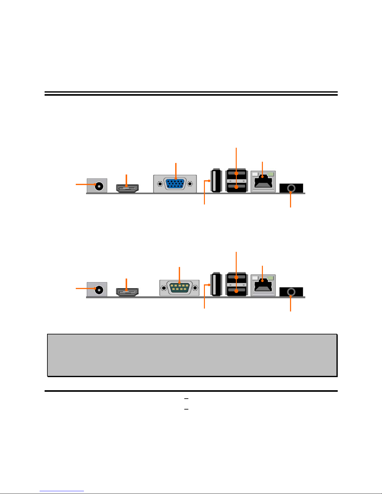
1-3 Layout Diagram
NF9KV Rear IO Diagram
NF9KC Rear IO Diagram
Warning!
The board has a DC 9-24V power connector (J1) in I/O back panel and an internal ATX12V
(DCCN1) power connector. User can only connect one type of compatible power supply to one
of them.
HDMI Port
VGA Port
9~24V
DC Power
Connector
USB 2.0 Port
Line Out/
Optical SPDIF_Out Connector
RJ-45 LAN Port
USB 2.0 Ports
HDMI Port
COM1 Port
9~24V
DC Power
Connector
USB 2.0 Port
Line Out/
Optical SPDIF_Out Connector
RJ-45 LAN Port
USB 2.0 Ports
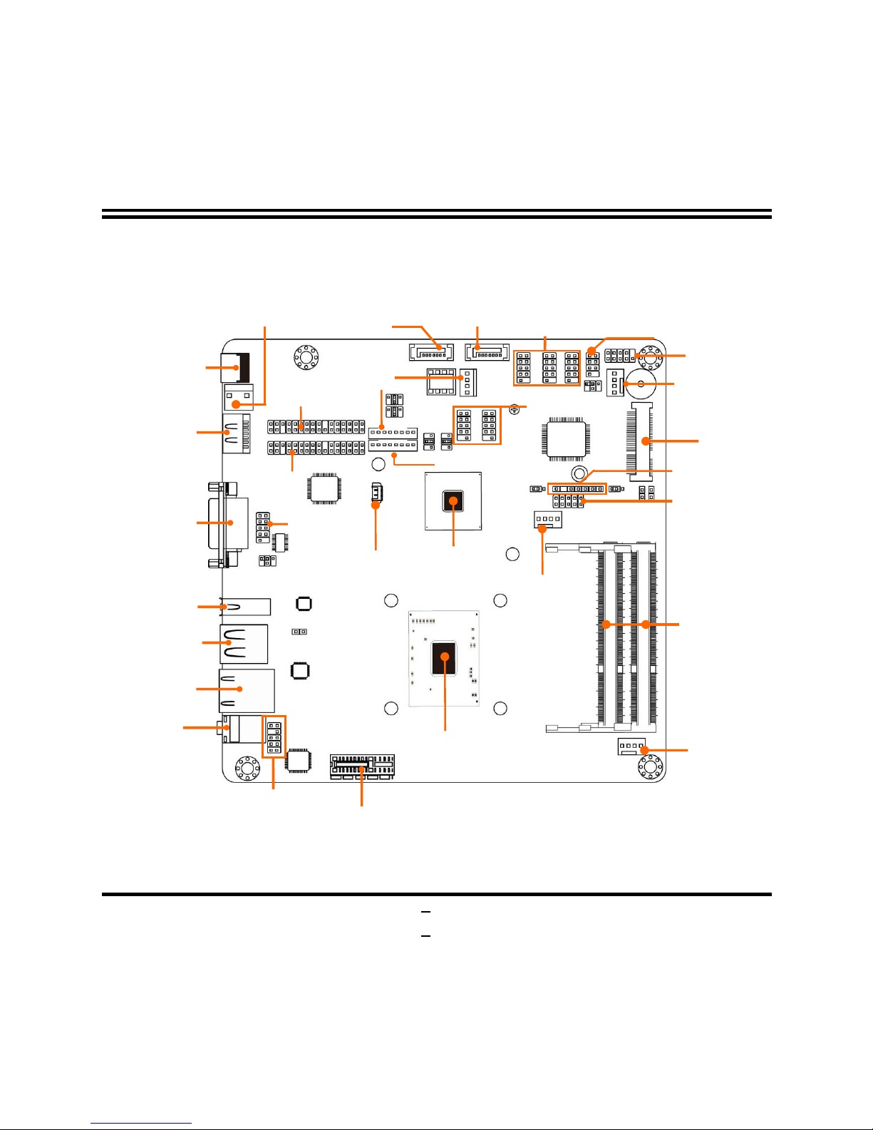
5
NF9KV: Motherboard Internal Diagram
9~24 VDC
Power Connector
(J1)
HDMI Port
VGA Port
USB 2.0 Port
RJ-45 LAN
Port
Line Out/Optical
SPDIF
_
out Connector
Front Panel Header
PS/2 KB/MS Header
CPU FAN Header
L
VDS1 Header
GPIO Heade
r
Intel CPU
Intel HM65
Chipset
PCI-Express x 1 Slot
USB 2.0 Headers
SYSFAN1 Header
SYSFAN2 Header
INVERTER2
Font Panel
Audio Header
DDRIII SO-DIMM Slots
Internal DC Power
Connector
(DCCN1)
Serial Port
Header (COM1)
USB 2.0 Ports
SATAII Port
(SATA2)
SATAIII Port
(SATA1)
Serial Port
Headers
(COM2/3/4)
Full-size
M
ini-PCIE/MSATA Slo
t
Power LED +
Speaker Header (J2)
INVERTER1
L
VDS2 Header
SATA HDD Power Connector
Battery Connector
6
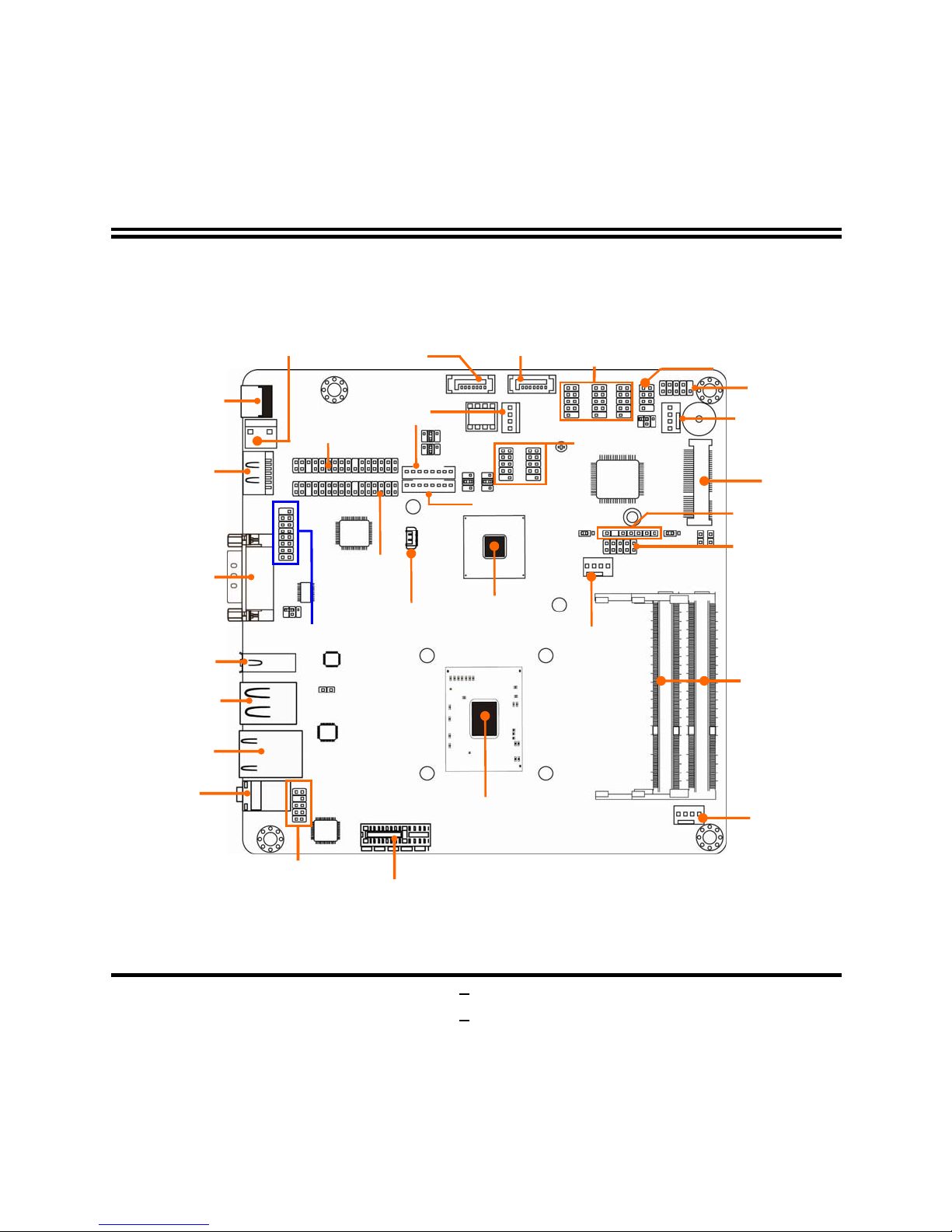
NF9KC: Motherboard Internal Diagram
9~24V DC
Power Connector
(J1)
HDMI Port
Serial Port
(
COM1)
USB 2.0 Port
RJ-45 LAN
Port
Line Out/Optical
SPDIF
_
out Connector
Front Panel Header
PS/2 KB/MS Header
CPU FAN Header
L
VDS1 Header
GPIO Heade
r
Intel CPU
Intel HM65
Chipset
PCI-Express x 1 Slot
USB 2.0 Headers
SYSFAN1 Header
SYSFAN2 Header
INVERTER2
Font Panel
Audio Header
DDRIII SO-DIMM Slots
Internal DC Power
Connector
(DCCN1)
VGA Port
Header (V GA)
USB 2.0 Ports
SATAII Port
(SATA2)
SATAIII Port
(SATA1)
Serial Port
Headers
(COM2/3/4)
Power LED +
Speaker Header (J2)
INVERTER1
L
VDS2 Header
SATA HDD Power Connector
Full-size
M
ini-PCIE/MSATA Slo
t
Battery Connector
7
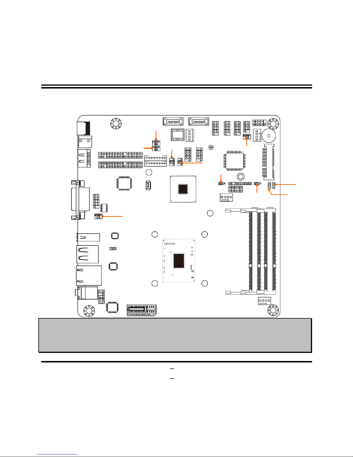
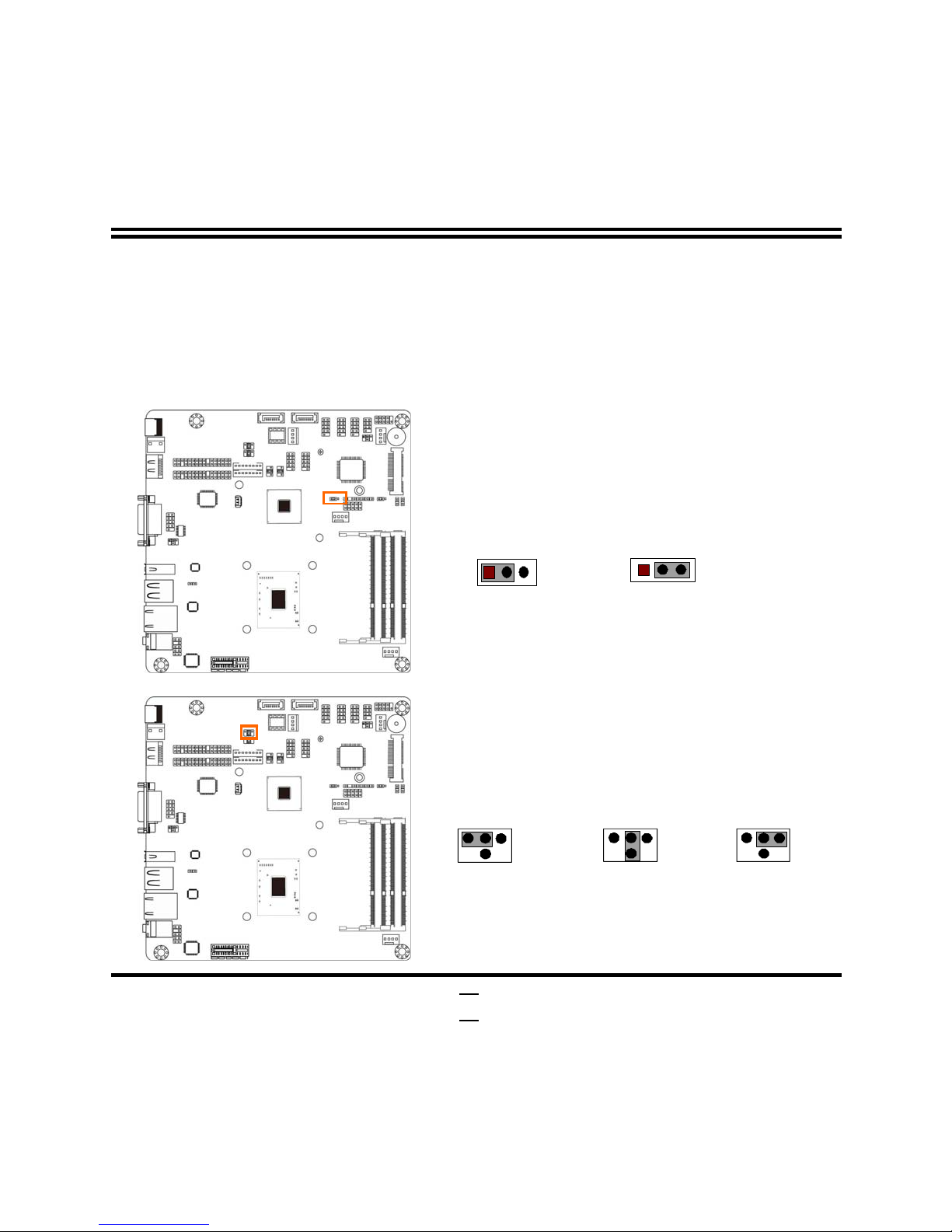
Motherboard Jumper Position
Note:
z
The above illustration diagram is from NF9KV.
z
NF9KC series has the same jumpers at the same marked positions.
z
The following diagrams for illustrations are from NF9KV as well, unless otherwise noted.
J
P2
JP1
JP3
JP4
JP5
AT_
MODE1
COPEN1

8
Jumper
Jumper Name Description
JBAT CMOS Clear Function Setting 3-pin Block
JP1 LVDS1 VCC 3.3V/5V/12V Select 4-pin Block
JP2 LVDS2 VCC 3.3V/5V/12V Select 4-pin Block
JP3 INVERTER2 VCC 3.3V/5V/VIN Select 4-pin Block
JP4 INVERTER1 VCC 3.3V/5V/VIN Select 4-pin Block
JP5 MINI_CARD Slot Power 3.3V/3.3VSB Select 3-Pin Block
JCOMP1 COM1 Port/Header Pin9 Function Select 4-Pin Block
JCOMP4 COM4 Header Pin9 Function Select 4-Pin Block
AT_MODE1 AT MODE Function Select 2-pin Block
COPEN1 Case Open Message Display Function 2-Pin Block
Connectors
Connector Name
J1 DC 9~24V Power Connector
DCCN1 Internal DC Power Connector
HDMI
High-Definition Multimedia Interface
VGA (for NF9KV) Video Graphic Attach Connector
COM1 (for NF9KC) Serial Port Connector
USB1 USB Port Connector
USB2 USB Port Connector x2
LAN1 RJ-45 LAN Connector
HP_SPDIF1 Line Out /Optical SPDIF Out Connector
PWOUT Power Out Connector
SATA1 SATAIII Connector
SATA2 SATAII Connector
CPUFAN;SYSFAN1;SYSFAN2 Internal Fan Connectors
9
Headers
Header Name Description
FP_AUDIO Front Panel Audio Header 9-Pin Block
NIC_LED2 LAN Activity LED Header
2-Pin Block
VGA1 (for NF9KC)
Video Graphic Attach Header 15-Pin Block
LVDS1/LVDS2 LVDS Header 30-Pin Block
INVERTER1/INVERT
ER2
LVDS Inverter 8-Pin Block
COM1 (for NF9KV);
COM2; COM3; COM4
Serial Port Headers 9-Pin Block
J2 PWELED Header + Speaker Header 7-pin Block
JW_FP1 Front Panel Header(PWR LED/ HD
LED/ /Power Button /Reset)
9-Pin Block
F_USB1/F_USB2 USB 2.0 Header 9-pin Block
PS2_CON1 PS/2 Keyboard & Mouse Header 6-Pin Block
GPIO_CON1 GPIO Header 10-Pin
10
Chapter 2
Hardware Installation
2-1 Jumper Setting
(1) JBAT (3-pin): Clear CMOS
CMOS Clear Setti ng
2-3 Closed:Clear CMOS
JBAT
1-2 Closed: Normal;
1
3
1
(2) JP1 (4-pin): LVDS1 VCC 3.3V/5V /12V Select
JP1→LVDS1
6-4 Closed: LVDS1
VCC= 12V;
642
3-4 Closed: LVDS1
VCC= 5V;
2-4 Closed: LVDS1
VCC= 3.3V
3
1
5
13
5
24
6
1 3
5
2 4 6
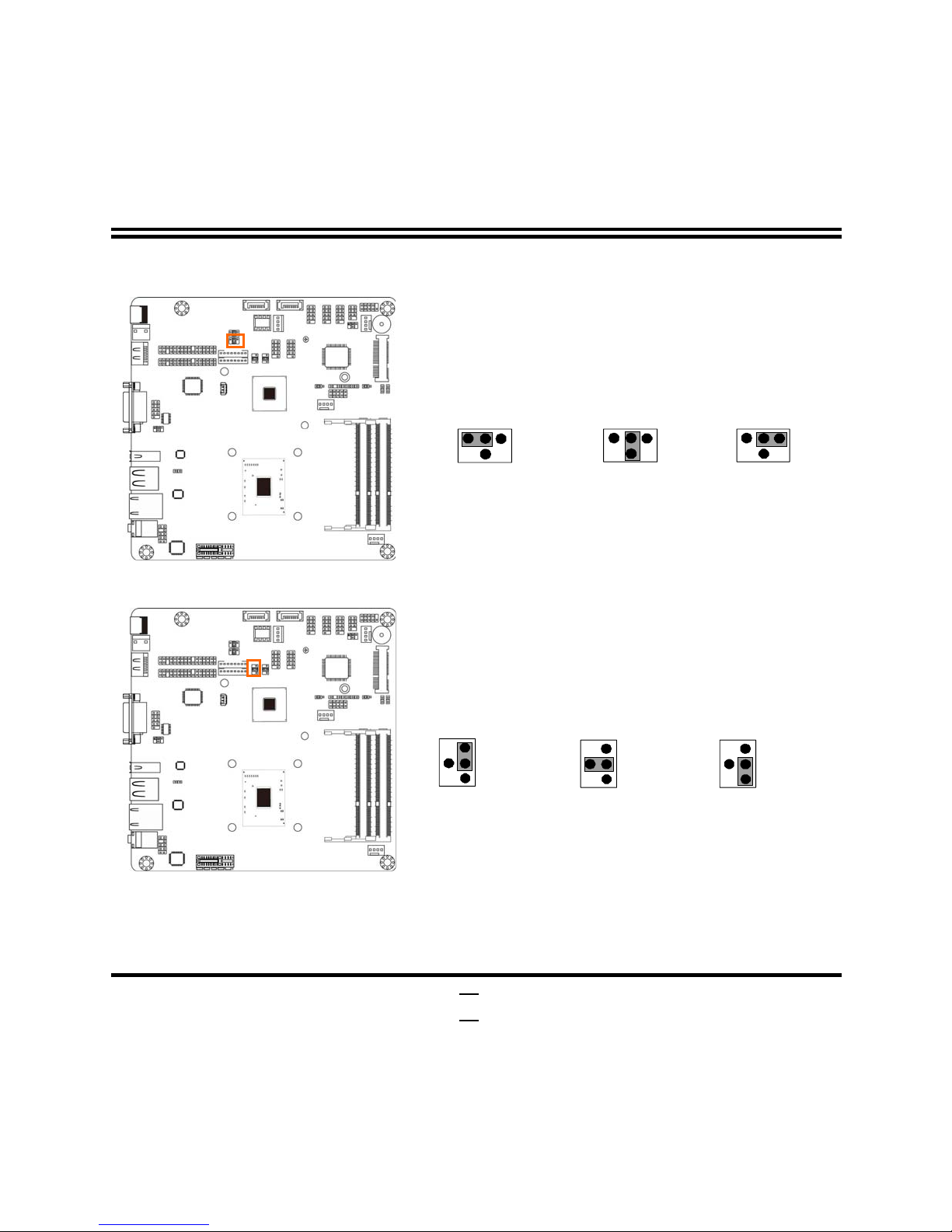
11
(3) JP2 (4-pin): LVDS2 VCC 3.3V/5V /12V Select
JP2→LVDS2
6-4 Closed: LVDS2
VCC= 12V;
642
3-4 Closed: LVDS2
VCC= 5V;
2-4 Closed: LVDS2
VCC= 3.3V
3
1
5
13
5
24
6
1 3
5
2 4 6
(4) JP3 (4-pin): INVERTER2 VCC 3.3V/5V/VIN Select
JP3→INVERTER2
6-4 Closed:
Invert er Back lig ht
VCC= VIN.
6
4
2
3-4 Closed:
Inve rte r Ba ckl ig ht
VCC= 12V;
2-4 Closed:
Inverter Backlight
VCC= 5V;
3
1
5
1
2
4
6
3
5
2
4
6
1
3
5
 Loading...