


J-530BF
USER'S MANUAL
3D-AGP VGA / 3D-Audio M/B
FOR Pentium processor
The author assumes no responsibility for any errors or omissions which
may a p p e a r in th i s d o cume n t n o r doe s i t m a ke a commitment to update
the information contained herein.
NO. G03-530BFRAA
Release date: SEP 2000
** Year 2000 compliant **
Trademark:
* Pentium is registered trademark and MMX is a trademark of Intel corporation,
the other names and brands are the property of their respective owners.
* Specifications and Information contained in this documentation are furnished for information use only, and are
subject to change at any time without notice, and should not be construed as a commitment by manufacturer.

i
Chapter 1
1-1 Preface...................................................................................................1
1-2 Key Feature ...........................................................................................1
Chapter 2
Hardware Installation........................................................................................3
2-1 Unpacking..............................................................................................3
2-2 Mainboard Layout.................................................................................4
2-3 Quick Reference for Jumpers, Connectors & Expansion Socket.....5
2-4 Installation Steps..................................................................................6
2-5 Jumper Settings....................................................................................6
2-6 System Memory (DRAM) ......................................................................8
2-7 Central Processing Unit (CPU) ............................................................ 9
2-8 Expansion Cards...................................................................................9
2-9 External Connectors.............................................................................9
Chapter 3
AWARD BIOS SETUP........................................................................................16
3-1 STANDARD CMOS SETUP ...................................................................17
3-2 BIOS FEATURES SETUP......................................................................18
3-3 CHIPSET FEATURES SETUP ...............................................................21
3-4 POWER MANAGEMENT SETUP ..........................................................24
3-4-1 The Description of the Power Management.............................26
3-4-2 Description of the Green Function ..........................................28
3-5 PNP/PCI CONFIGURATION SETUP ......................................................29
3-6 LOAD BIOS DEFAULTS.........................................................................30
3-7 LOAD SETUP DEFAULTS......................................................................31
3-8 INTEGRATED PERIPHERALS SETUP .................................................. 31
3-9 SUPERVISOR/USER PASSWORD.........................................................33
3-10 IDE HDD AUTO DETECTION ...............................................................34
3-11 SAVE & EXIT SETUP............................................................................35
3-12 EXIT WITHOUT SAVING.......................................................................35
3-13 I/O & MEMORY MAP ............................................................................36
3-14 TIME & DMA CHANNELS MAP............................................................37
3-15 INTERRUPT MAP..................................................................................37
3-16 RTC & COMOS RAM MAP ...................................................................37
3-17 BIOS REFERENCE-POST CODES.......................................................38
Chapter 4
4-1 Sound Card Driver Quick Installation..................................................... 42
4-2 Display Card Driver Quick Installation ...................................................43
4-3 PC HEALTH MONITOR-II SOFTWARE.....................................................43
APPENDIX-A Magic Install
TABLE OF CONTENT

1
Chapter 1
1-1 Preface
Welcome to use the J-530BF mainboard. This mainboard is based on Pentium
processor PC/AT compatible system with ISA bus and PCI local bus. Also for this board
including some special designs like, support 100MHz frequency, 3D AGP VGA chip, 3D
PCI Audio chip, ACPI/AMP power management & powerful performance and so on. We
think you will enjoying your personal computer because of your right choice.
1-2 Key Feature
The J-530BF is design for the PC user who wants a great many features in a small
package . This motherboard :
Support 100MHz Bus Frequency for AMD-K6-2/300/350/400, AMD-K6-3/400/450
.
Support SDRAM clock selectabled in 100MHz by jumper setting let user more
choice when use SDRAM.
Built-In High performance 3D AGP VGA:
Support share memory 2MB to 8MB selectable in BIOS SETUP.
64 bits memory data interface.
Integrated programmable 24-bit true-color RAMDAC up to 230MHz pixel clock.
Integrated two 96x64 video line buffers for MPEG video playback.
Support 64 bit memory data bus interface.
Integrated a high performance and high quality 3D engine.
Support DIC, Direct Draw Driver.
Support AGP Spec.1.0 compliant, 1xmode(66MHz), 2xmode(133MHz)
Built-In High performance 3D PCI Audio:
Support PCI Bus Spec 2.1 compliant.
Full native DOS games compatibility via three technologies:
TDMA(Transparent DMA), DDMA(Distributed DMA), PC/PCI.
High-Quality ESFM music synthesizer.
Integrated 3D audio effect processor.
Full-duplex operation for simultaneous record and playback.
Meets PC 97/98 and WHQL Specifications.
Multi-Speed Support :
support 66/75/83/95/100MHz Host Bus Frequency for Intel
Pentium processor with MMX technology ,AMD K5/K6/K6-2/K6-3,Cyrix 6x86
M1/M2,IDT Winchip CPU on a ZIF Socket7.
Chipset:
SiS 530/5595 AGPset chip with I/O subsystems, and ESS 1938S 3D PCI
Audio chip.
L2 Cache :
Provide on board 512K Pipelined Burst SRAM to increase system
performance.
DRAM Memory Support:
support 3 168-pin DIMMS(3.3V)from a memory size befween
8MB to 768MB.

2
ISA and PCI ecpansion Slots:
Privodes two 16-bit ISA slots, three PCI slots.
Super Multi-I/O:
Provides two high-Speed UART compatible serial ports and one
parallel port with EPP and ECP capabilities. UART2 can also be directed to the
Infrared Module for wireless connections. Two floppy drives of either 5.25” or 3.5”
(1.44MB or 2.88MB) are also supported without an external card.
PCI Bus Master IDE Controller and ULTRA DMA 33:
On-board PCI Bus Master IDE
controller with two connectors that supports four IDE devices in two channels, provides
faster data transfer rates, and supports Enhanced IDE devices such as Tape Backup,
CD-ROM drives and LS-120. This controller also supports PIO Modes 3 and 4 and Bus
Master IDE DMA 33Mbyte/Sec.
ACPI supporting for OS Directed Power Management
Ring-in Wake up:
When Ring-In the system can wake up from SMI Mode.
Ring-in Power On:
When Ring-In the system can power on automatic by this function
by use of ATX power supply.
RTC Power On:
When use of ATX power supply and Enabled RTC Power On function,
you can setting RTC alarm to power on the system at the time length you setting .
Power Button:
Press the button will place the system power on/off when use ATX
power supply .
Software off when use ATX power supply.
Power Support:
Efficient PWM switching power instead of traditional Linear Voltage
Regulator to prevent power component from being burned-out.
Meets PC99 Requirements.
Optional IRDA and PS/2:
This motherboard supports an optional infrared port module
for wireless interface and PS/2 mouse cable set.
Opti ona l USB Port Connector:
This motherboard supports two USB port conne ctors for
USB devices.
Bundle with “Xstore Pro” High Performance ULTRA DMA 33 Driver to improve
IDE transfer rate up to 33Mbyte/sec. Increase System Performance 10% more,
Hard Drive performance 60% more.
Baby AT Form Factor:
Dimensions 22cm x 22cm.

3
Chapter 2
Hardware Installation
2-1 Unpacking
This mainboard package should contain the following:
The J-530BF mainboard
USER’S MANUAL for mainboard
Cable set for IDE x1, Floppy x1, COM1 & COM2 x1, LPT & PS/2 Mouse x1, VGA
x1,Audiox1
CD for Drivers PACK
The mainboard contains sensitive electronic components which can be easily damaged by
electron-static, so the mainboard should be left in its original packing until it is installed.
Unpacking and installation should be done on a grounded anti-static mat.
The operator should be wearing an anti static wristband, grounded at the same point as
the anti-static mat.
Inspect the mainboard carton for obvious damage. Shipping and handling may cause
damage to your board. Be sure there are no shipping and handling damages on the board
before proceeding.
After opening the mainboard carton, extract the system board and place it only on a
grounded anti-static surface component side up. Again inspect the board for damage.
Press down on all of the socket IC’s to make sure that they are properly inserted. Do this
only on with the board placed on a firm flat surface.
Warning: Do not apply power to the board if it has been damaged.
You are now ready to install your mainboard. The mounting hole pattern on the
mainboard matches the IBM-AT system board.
It is assumed that the chassis is designed for a standard IBM XT/AT main board
mounting. Place the chassis on the anti-static mat and remove the cover.
Take the plastic clips, Nylon stand-off and screws for mounting the system board, and
keep them separate.
4
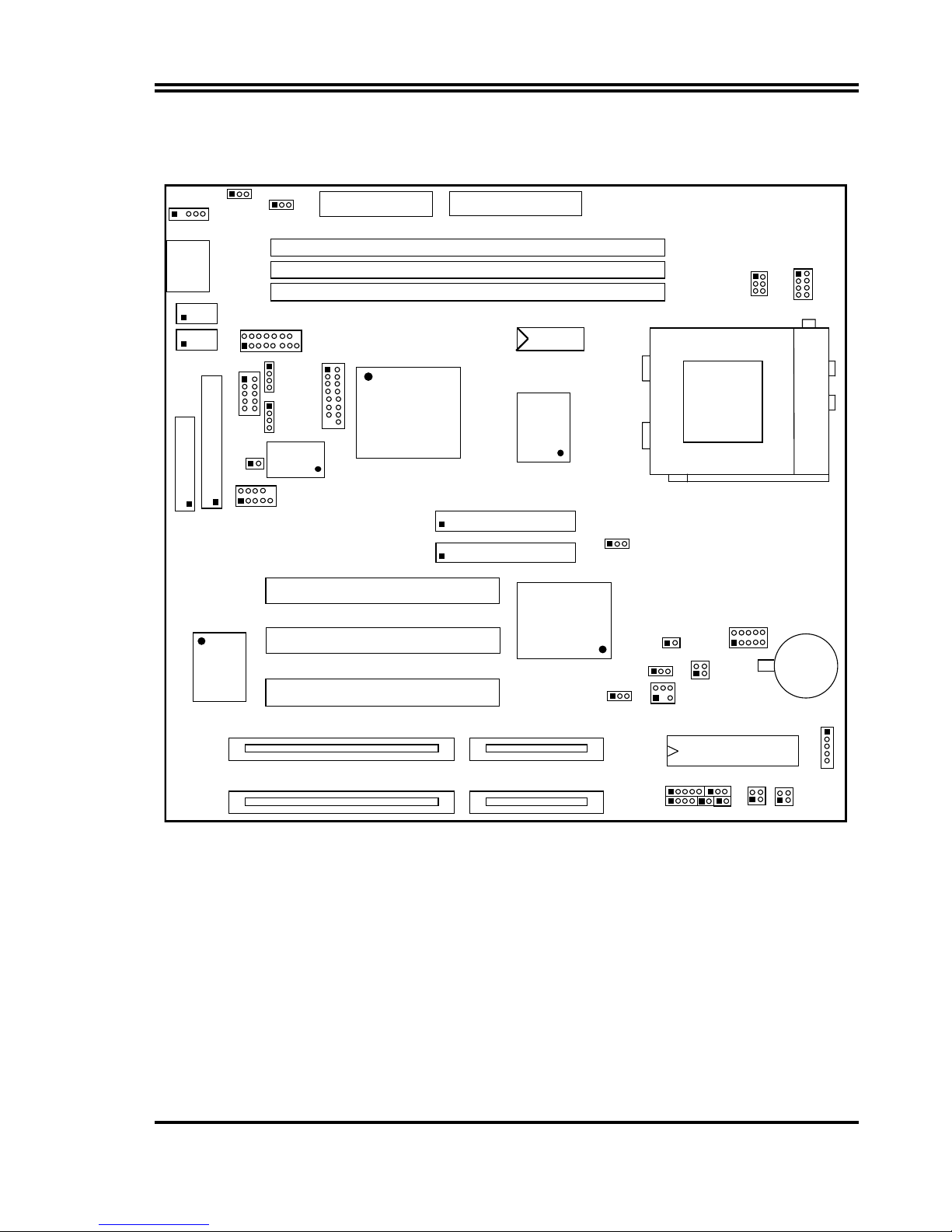
2-2 Mainboard Layout
J
2
K/B
CONN.
ZIF SOC KE T 7
CPU
A
T POWER CONN.
PW2
FDD1
2
1
2
1
2
39
40
39
40
LPT1
U4
PW1
ATX POWER CONN.
COM
2
COM1
64K X 64
SL
2
SL1
USB1
2
1
10
9
+
J1
1
PCI 2
PCI
3
PCI 1
WOL
13
BIO
S
JP6
SYS
FAN1
13
ITE 8661
F
U18
2
1
2 4
JP9
1 3
KEYLOCK TBS
W
SPEA KER RST T BLED
PS-ON
JP13
JP4
JP8
HDLED
SMI
E S 1938S
JP1
13
AUDI
O
U24
GAM
E
VGA 1
IR1
1
32K X
8
JP3
JP2
1
JP11
JP1
2
Figure 2-1
2-3 Quick Reference for Jumpers, Connectors &
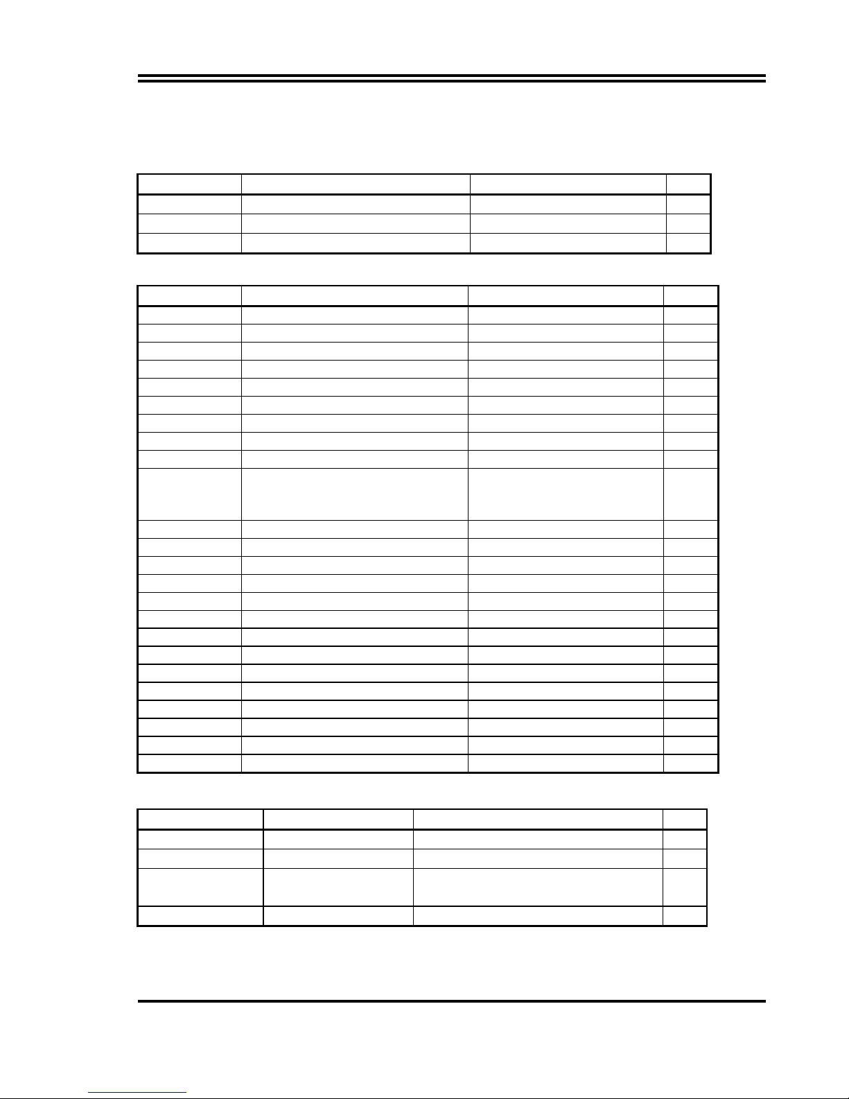
5
Expansion Socket
Jumpers
Jumper Name Description Page
JP6 CMOS RAM Clear 2-3 Normal ,1-2 Clear CMOS p. 8
JP8 CPU Voltage selector for detail page 7 p. 6
JP2,JP3 Jumpers for CPU type selection for detail page 7 p. 6
Connectors
Connector Name Description Page
J2 Keyboard Connector 5-Pin Female p.10
USB1 USB Port Connector 10-Pin Block p.13
J1 PS/2 Mouse Connector 6-Pin Block p.10
COM1,COM2 Serial Port COMA & COMB 10-Pin Block p.11
LPT1 Parallel Port Connector 26-Pin Block p.11
FDD1 Floppy Driver Connector 34-Pin Block p.11
IDE1 Primary IDE Connector 40-Pin Block p.11
IDE2 Secondary IDE Connector 40-Pin Block p.12
VGA1 VGA Connector 16-Pin Block p.14
CPUFAN1
SYSFAN1
FAN Connector 1-2 12V Power Connector
2-3 ACPI FAN power control
Connector
p.13
IR1 Infrared Module Connector 5-Pin Block p.13
PW2 AT Power Connector 12-Pin Block p. 9
PW1 ATX Power Connector 20-Pin Block p.410
HDLED IDE activity LED 2-Pin Connector p.12
FPC Front Panel Connector 16-Pin Block
p.12
PS-ON ATX power button/soft power button 2-Pin connector p.13
Audio Audio connector 10-pin connector p.14
Game Game port connector 16-pin connector p.14
JP12 CD-Audio/Panasonic 4-pin Block p.14
JP11 CD-Audio/Sony/IDE 4-pin Block p.14
WOL Wake On Lan 3-pin Block p.15
JP13 Audio chip Enabled/Disabled On-Enabled , Off-Disabled p.15
J5 SB_Link connector 6-pin connector p.15
JP1 Keyboard Voltage selector 1-2 : 5VSB , 2-3 : Vcc p.15
Expansion Sockets
Socket/Slot Name Description Page
SL1, SL2 ISA Slot 16-bits ISA Bus Expansion slots p.9
PCI1, PCI2, PCI3 PCI Slot 32-bits PCI Local Bus Expansion slots p.9
DIMM1,DIMM2,
DIMM3
DIMM Module Socket 168-Pins DIMM SDRAM Module
Expansion Socket
p.8
ZIF SOCKET 7 CPU Socket Pentium CPU Socket p.9
2-4 Installation Steps
6
Before using your computer, you must follow the steps as follows:
1. Set Jumpers on the Motherboard
2. Install the CPU
3. Install DRAM Modules
4. Install Expansion card
5. Connect Cables, Wires, and Power Supply
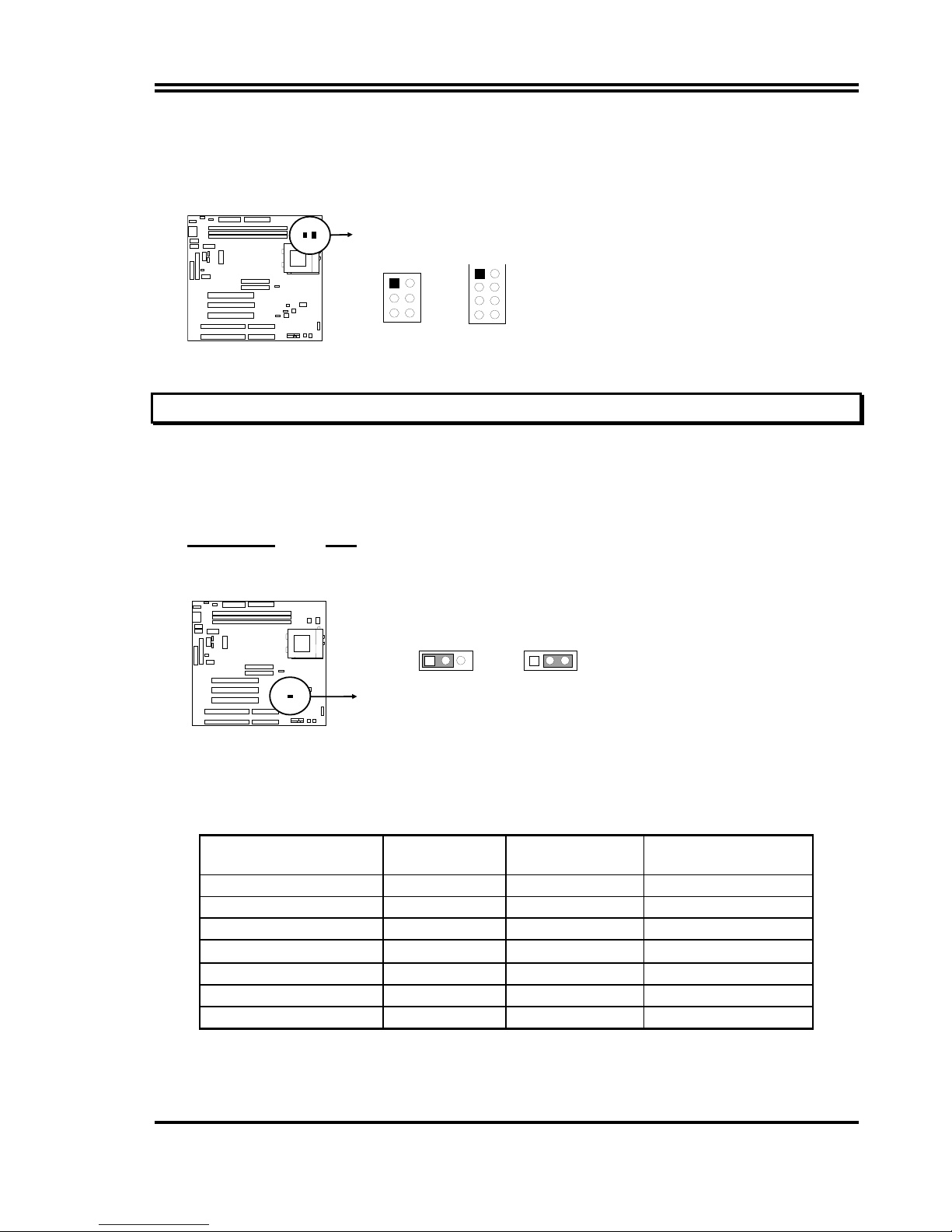
2-5 Jumper Settings
1. CPU Voltage Selection: JP8 (2x5pin Block)
This jumper is used for adjusting CPU working voltage, for this main board design it
can auto detect the single voltage CPU or dual voltage CPU.
The table of JP8 CPU voltage selection {S : short (ON) , O : open (OFF)}
JP8 1-2 3-4 5-6 7-8 9-10
1.8V O S O S S
2.0V O S S S S
2.1V S O O O O
2.2V O S O O O
2.3V S S O O O
2.4V O O S O O
2.5V S O S O O
2.8V O O O S O
2.9V S O O S O
3.1V S S O S O
3.2V O O S S O
3.3V S O S S O
3.5V S S S S O
If your CPU Type is not including in above table, please refer to the CPU voltage selection
on below to choose the correct working voltage for your CPU.
CPU Voltage Selection
1.8V
JP8
1
2
9
10
2.0V
JP8
1
2
9
10
2.8V
JP8
1
2
9
10
2.9V
JP8
1
2
9
10
3.1V
JP8
1
2
9
10
3.2V
JP8
1
2
9
10
3.3V
JP8
1
2
9
10
3.5V
JP8
1
2
9
10
2.2V
JP8
1
2
9
10
2.5V
JP8
1
2
9
10
2.4V
JP8
1
2
9
10
2.3V
JP8
1
2
9
10
2.1V
JP8
1
2
9
10
2. CPU Type selection: JP2 &JP3
This mainboard designs JP2 to select the CPU, external clock (Host Bus Frequency)
and JP3 to select the CPU Bus Frequency ratio, the external clock frequency
multiplied by Bus frequency ratio is the CPU frequency as the tables below:
Table for CPU external frequency / SDRAM Clock setting : JP2
SD FS2 FS1 FS0 CPU Bus Clock SDRAM Clock
7
O S S S 66.8 MHz 66.8 MHz
O S S O 75 MHz 75 MHz
O S O S 83.3 MHz 83 MHz
O S O O 95 MHz 95 MHz
O O S S 100 MHz 100 MHz
O O S O 112 MHz 112 MHz
S S S S 90/66.8 MHz 90/89 MHz *
S S S O 83.3 MHz 66.8 MHz *
S S O S 95 MHz 63.3 MHz *
S S O O 100 MHz 66.6 MHz *
S O S S 100/105 MHz 75 MHz *
S O S O 112 MHz 74.4 MHz *
※
SDRAM Clock Asynchronous as CPU Bus frequency let user can use slow
speed SDRAM when CPU clock over 83MHz.{ S : short (ON) O : open (OFF) }
For ICS9248-81 clock Generator
Table for CPU ratio selector : JP3
CPU ratio BF0 BF1
BF2
1.5 X / 3.5 X OFF OFF OFF
2.0 X ON OFF OFF
2.5 X ON ON OFF
3.0 X OFF ON OFF
4.0 X ON OFF ON
4.5 X ON ON ON
5.0 X OFF ON ON
5.5 x OFF OFF ON
Table for CPU Type selection :
JP2 (Bus clock) JP3 (clock ratio)
CPU Type
SD FS2 FS1 FS0 BF0 BF1 BF2
Bus clock
Clock ratio
233MHz Pentium processor
with MMX technology
AMD K6-233
Cyrix 6X86 MII 300
O S S S O O O 66MHz 3.5X
200MHz Pentium processor
with MMX technology
AMD K6-200
Cyrix/IBM 6X86 MII 233
O S S S O S O 66MHz 3.0X
AMD K6/266, K6-2/266 O
S S S S O S 66MHz 4.0X
AMD K6/300 O S S S S S S 66MHz 4.5X
AMD K6-2/300 O O S S O S O 100MHz 3.0X
AMD K6-2/333 O S O O O O O 95MHz 3.5X
AMD K6-2/350 O O S S O O O 100MHz 3.5X
AMD K6-2/400, K6-3/400 O O S S S O S 100MHz 4.0X
AMD K6-2/450, K6-3/450 O O S S S S S 100MHz 4.5X
AMD K6-2/500, K6-3/500 O O S S O S S 100MHz 5.0X
AMD K6-2/550, K6-3/550 O O S S O O S 100MHz 5.5X
Cyrix MII-266 O S O S S S O 83MHz 2.5X
Cyrix MII-333 O S O S O S O 83MHz 3.0X
Cyrix MII-333 O S S O O O O 75MHz 3.5X
Cyrix MII-366 O O S S S S O 100MHz 2.5X
Cyrix MII-400 O S O O O S O 95MHz 3.0X
Cyrix MII-433 O O S S O S O 100MHz 3.0X
IDT Winchip-225 O S S O O S O 75MHz 3.0X
8
NOTE: c Before installing the CPU, Please check the CPU Frequency and Clock Ratio from
your supplier.
d
For Cyrix/IBM 6X86MX series, please double check the CPU’s Frequency and
Clock Ratio.
JP3
1
JP2
1
3. CMOS RAM Clear: JP6 (Yellow color selector)
WARNING: Make sure your computer is POWER OFF when you CLEAR CMOS.
Connect a jumper Cap over this jumper for a few seconds, will clears information
stored in the CMOS RAM Chip that input by user, such as hard disk information and
passwords. After CLEAR CMOS, you must enter the BIOS setup (by holding down
<DEL> during power-up) to re-enter BIOS information (see BIOS SETUP).
Selections
JP6
Normal 2-3 (Default)
Clear CMOS 1-2 (momentarily)
Normal
CMOS RAM (Normal / Clear CMOS Data)
JP6
123
Clear CMOS
JP6
123
2-6 System Memory (DRAM)
This main board supports three 168-pins DIMM modules, the Max Memory Size is 768MB
Because of the VGA share memory function, the system must always occupy BANK0
(DIMM1)to booting.
DIMM 1 DIMM 2 DIMM 3
System can be
Accept or Not
168-pin DIMM
Accept
168-pin DIMM 168-pin DIMM
Accept
168-pin DIMM
168-Pin DIMM
Accept
168-pin DIMM 168-pin DIMM 168-pin DIMM
Accept
168-pin DIMM
Not Accept
168-pin DIMM
Not Accept
168-pin DIMM 168-pin DIMM
Not Accept
The SDRAM clock can choice Synchronous(# SD open) or Asynchronous(# SD
closed) by the jumper setting of JP2, let user more choice of SDRAM .
9
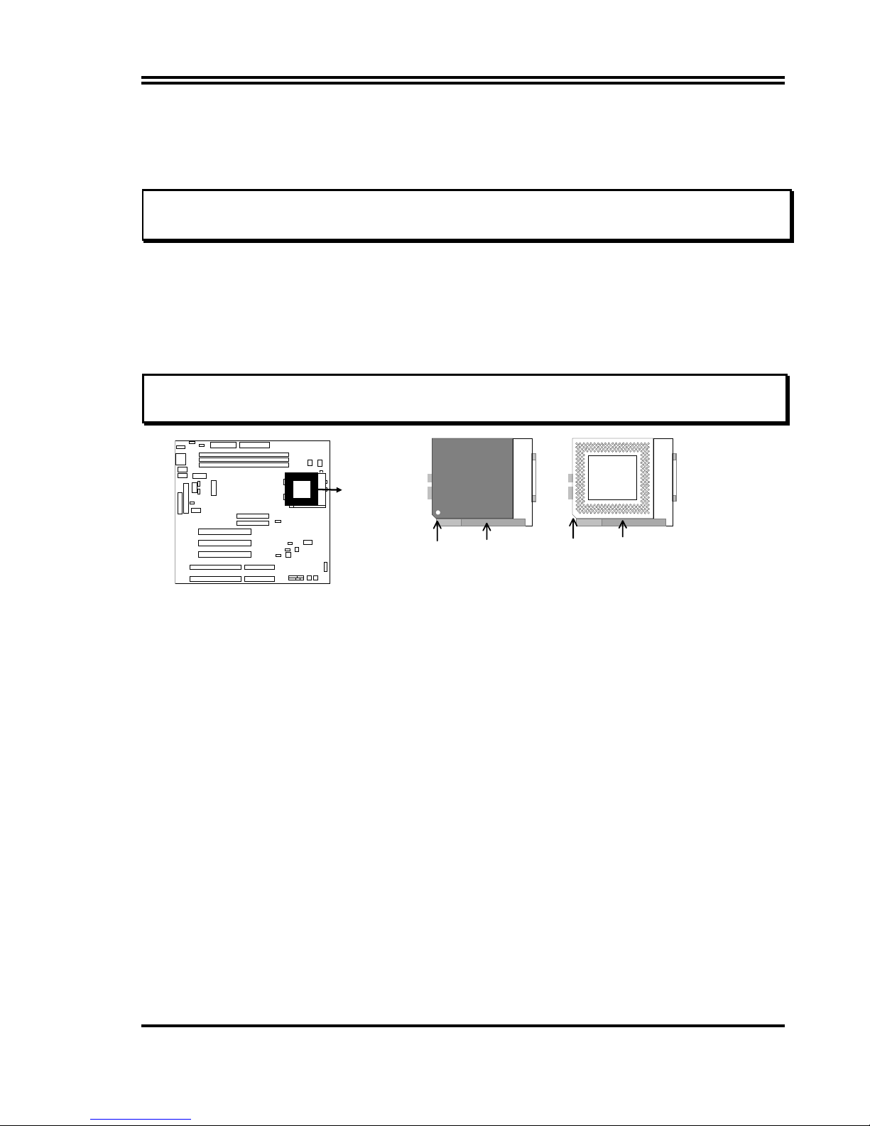
2-7 Central Processing Unit (CPU)
The main board provides a 321-pins ZIF Socket 7. The CPU on mother board must have
a fan attached to prevent overheating.
WARNING: Without a fan, the CPU will be overheated and cause damage to both the CPU
and the motherboard.
To install a CPU, first turn off your system and remove its cover. Locate the ZIF socket
and open it by first pulling the lever sideways away from the socket then upwards to a 90degree right angle. Insert the CPU with the white dot as your guide. The white dot should
point towards the end of the level. The CPU has a corner pin for three of the four corners,
the CPU will only fit in the one orientation as shown as follow. With the added weight of
the CPU fan, no force is required to insert the CPU. Once completely inserted, hold down
on the fan and close the socket’s lever.
IMPORTANT: You must set jumpers JP2,JP3 “CPU Type selector” on page 5 and jumper JP8 “CPU
Voltage Selection” on page 5 depending on the CPU that you install.
CPU ZIF Socket 7
Lock
Socket 7
Blank
Socket 7
Lever
White Dot
CPU
2-8 Expansion Cards
First read your expansion card documentation on any hardware and software settings that
may be required to setup your specific card.
Installation Procedure:
1. Read the documentation for your expansion card.
2. Set any necessary jumpers on your expansion card.
3. Remove your computer’s cover.
4. Remove the bracket on the slot you intend to use.
5. Carefully align the card’s connectors and press firmly.
6. Secure the card on the slot with the screw you remove in step 4.
7. Replace the computer’s cover.
8. Setup the BIOS if necessary.
9. Install the necessary software drivers for your expansion card.
2-9 External Connectors
1. Power connector: AT Power Connector (12-pin block): PW2
This connector connects to a standard AT power supply. To connect the leads from
the power supply, ensure first that the power supply is not plugged. Most power
supplies provide two plugs (P8 and P9), each containing six wires, two of which are
black. Orient the connectors so that the black wires are located in the middle.
10
Using a slight angle, align the plastic guide pins on the lead to thei r rec eptac les on the
connector. Once aligned, press the lead onto the connector until the lead locks into
place.
Power Plugs f rom Power Suppl y
Power Connector on Motherboard
PG +12V
GND
+5V -12V -5V
+5V
P8 P9
O
RYBBBBBWRRR
2. Power Connector: ATX Power Connector (20-pin block): PW1
ATX Power Supply connector. This is a new defined 20-pins connector that usually
comes with ATX case. The ATX Power Supply allows to use soft power on
momentary switch that connect from the front panel switch to 2-pins Power On jumper
pole on the motherboard. When the power switch on the back of the ATX power
supply turned on, the full power will not come into the system board until the front
panel switch is momentarily pressed. Press this switch again will turn off the power to
the system board.
PIN ROW2 ROW1
1 3.3V 3.3V
2 -12V 3.3V
3 GND GND
4 Soft Power On 5V
5 GND GND
6 GND 5V
7 GND GND
8 -5V Power OK
9 +5V +5V (for Soft Logic
)
Pin 1
3. Keyboard Connector (5-pin female): J2
This connection is for a standard IBM-compatible keyboard. May also be known as a
101 enhanced keyboard.
Keyboard Connector (5-pins female )
Connector Plug from Keyboard
4. PS/2 Mouse Connector (6-pin block): J1
If you are using a PS/2 mouse, you must purchase an optional PS/2 mouse set which
connects to the 6-pins block and mounts to an open slot on your computer‘s case.
1: DATA
2: NC
3: GND
4: VCC
5: CLK
PIN 1
PS/2 Mouse Module Connec tor
* Please don’t turn off / on power
supply two quickly ,we recommend
aleast wait 4sec before turn on the
power , to protect the system
11
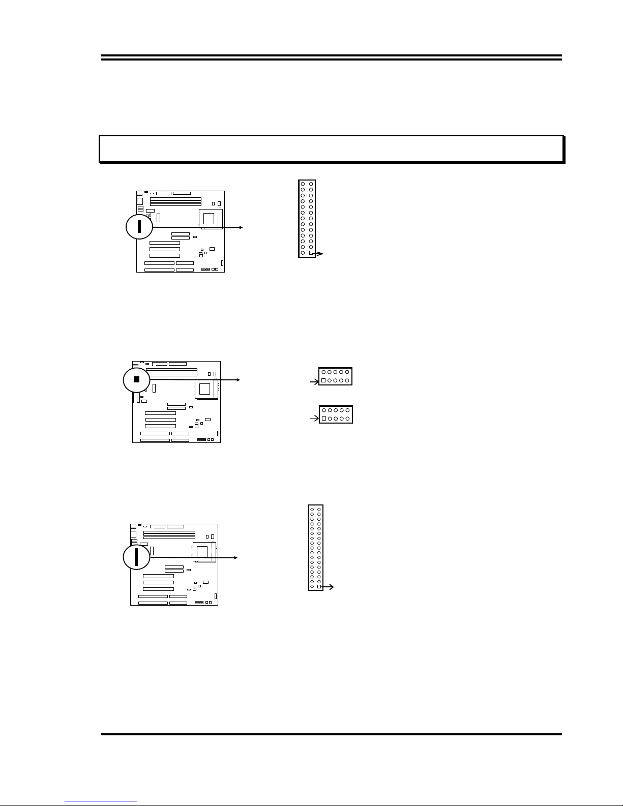
5. Parallel Printer Connector (26-pin Block): LPT1
Connection for the enclosed parallel port ribbon cable with mounting bracket. Connect
the ribbon cable to this connection and mount the bracket to the case on an open slot.
It will then be available for a parallel printer cable.
NOTE: Serial printers must be connected to the serial port. You can enable the parallel port and choose
the IRQ through BIOS Setup.
Pin 1
Parallel Printer Connector
LPT1
6. Serial port COMA and COMB Connector (Two 10-pin blocks): COM1, COM2
T he se connectors support the provided serial port ribbon cables wit h mounting bracket.
Connect the ribbon cables to these connectors and mount the bracket to the case on
an open slot. The two serial ports on the mounting bracket will then be used for
pointing devices or other serial devices. See BIOS configuration of “Onboard Serial
Port”
COM 1
Pin 1
Pin 1
COM 2
Serial port COMA and COMB Connector
7. Floppy drive Connector (34-pin block): FDD1
This connector supports the provided floppy drive ribbon cable. After connecting the
single plug end to motherboard, connect the two plugs at other end to the floppy
drives.
Pin 1
Flo
ppy
Drive Connector
FDD1
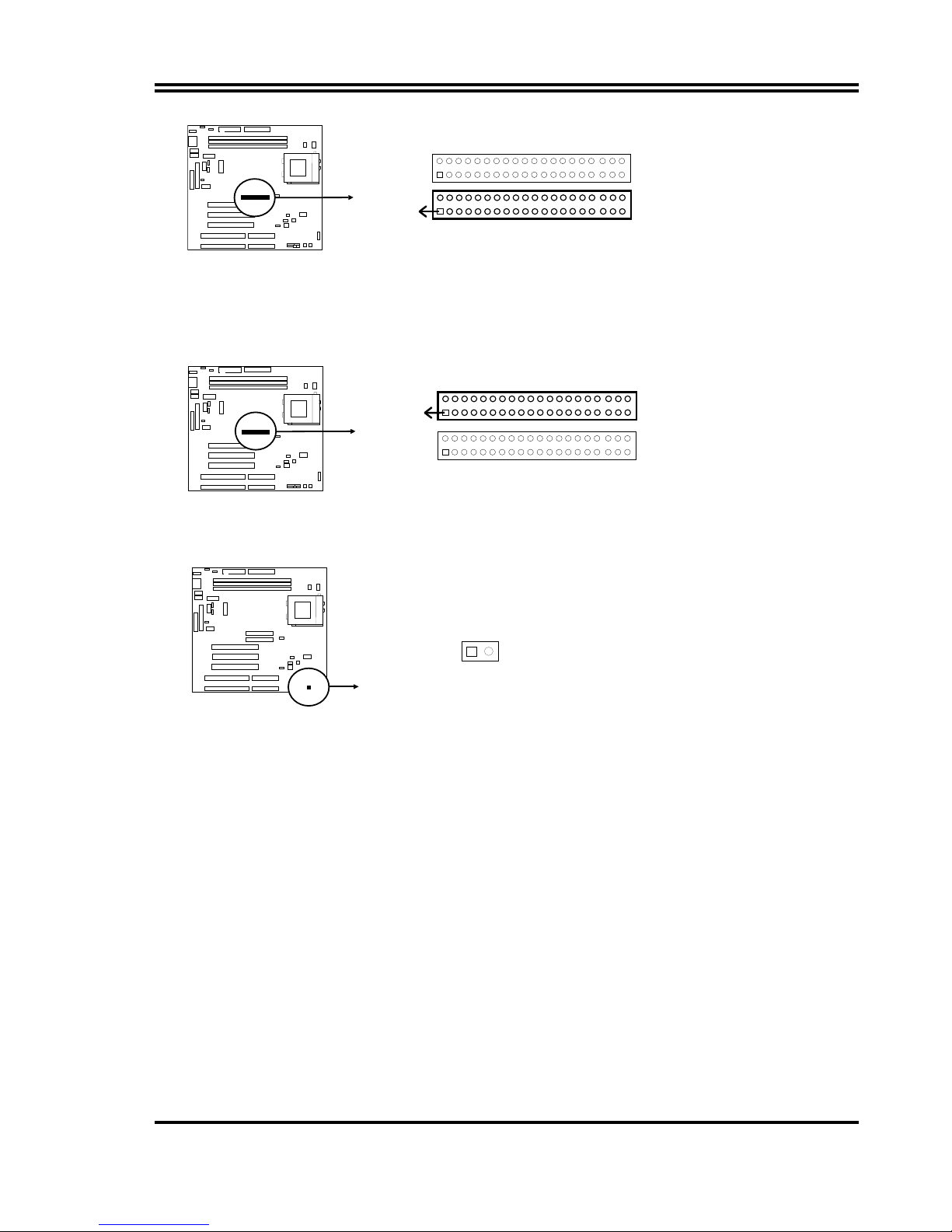
8. Primary IDE Connector (40-pin block): IDE1
This connector supports the provided IDE hard disk ribbon cable. After connecting the
single plug end to motherboard, connect the two plugs at other end to your hard
disk(s). If you install two hard disks, you must configure the second drive to Slave
mode by setting its jumpers accordingly. Please refer to the documentation of your
hard disk for the jumper settings.
12
Primary IDE Connector
Pin 1
9. Secondary IDE Connector (40-pin block): IDE2
This connector connects to the next set of Master and Slave hard disks. Follow the
same procedure described for the primary IDE connector. You may also configure
two hard disks to be both Masters using one ribbon cable on the primary IDE
connector and another ribbon cable on the secondary IDE connector.
Secondary IDE Connector
Pin 1
10. IDE activity LED: HDLED
This connector connects to the hard disk activity indicator light on the case.
HDLED
IDE (Hard Drive) LED
-
+
31
11. Front Panel connector:
This 16-pin connector to connect to case front panel switch.
A. Turbo LED switch: TBLED
The motherboard‘s turbo function is always on. The turbo LED will remain
constantly lit while the system power is on. You may also to connect the Power
LED from the system case to this lead. See the figure below.
B. Reset switch lead: RST
This 2-pin connector connects to the case-mounted reset switch for rebooting your
computer without having to turn off your power switch. This is a preferred method
of rebooting in order to prolong the life of the system‘s power supply. See the
figure below.
C. Keyboard lock switch lead & Power LED: KEYLOCK & PW
This 5-pin connector connects to the case-mounted key switch for locking the
keyboard for security purposes and Power LED together.
D. Speaker connector: SPEAKER
This 4-pin connector connects to the case-mounted speaker. See the figure below.
 Loading...