

Page 1

NF791 Series
User’s Manual
G03-NF791-F
Revision: 1.0
Release date: September 28, 2017
Trademark:
* Specifications and Information contained in this documentation are furnished for information use only, and are
subject to change at any time without notice, and should not be construed as a commitment by manufacturer.
Page 2

ii
Environmental Protection Announcement
Do not dispose this electronic device into the trash while discarding. To minimize
pollution and ensure environment protection of mother earth, please recycle.
Page 3

iii
ENVIRONMENTAL SAFETY INSTRUCTION ....................................................................... iv
USER’S NOTICE.................................................................................................................. v
MANUAL REVISION INFORMATION................................................................................... v
ITEM CHECKLIST................................................................................................................ v
CHAPTER 1 INTRODUCTION OF THE MOTHERBOARD
1-1 FEATURE OF MOTHERBOARD ............................................................................ 1
1-2 SPECIFICATION .................................................................................................... 2
1-3 LAYOUT DIAGRAM ............................................................................................... 3
CHAPTER 2 HARDWARE INSTALLATION
2-1 JUMPER SETTING................................................................................................. 9
2-2 CONNECTORS AND HEADERS............................................................................ 15
2-2-1 CONNECTORS ......................................................................................... 15
2-2-2 HEADERS................................................................................................. 20
CHAPTER 3 INTRODUCING BIOS
3-1 ENTERING SETUP................................................................................................. 29
3-2 BIOS MENU SCREEN............................................................................................ 30
3-3 FUNCTION KEYS................................................................................................... 30
3-4 GETTING HELP...................................................................................................... 31
3-5 MEMU BARS.......................................................................................................... 31
3-6 MAIN MENU ........................................................................................................... 32
3-7 ADVANCED MENU ................................................................................................ 33
3-8 CHIPSET MENU..................................................................................................... 46
3-9 SECURITY MENU .................................................................................................. 49
3-10 BOOT MENU.......................................................................................................... 50
3-11 SAVE & EXIT MENU .............................................................................................. 51
TABLE OF CONTENT
Page 4

iv
Environmental Safety Instruction
Avoid the dusty, humidity and temperature extremes. Do not place the product in
any area where it may become wet.
0 to 60 centigrade is the suitable temperature. (The figure comes from the request
of the main chipset)
Generally speaking, dramatic changes in temperature may lead to contact
malfunction and crackles due to constant thermal expansion and contraction from
the welding spots’ that connect components and PCB. Computer should go
through an adaptive phase before it boots when it is moved from a cold
environment to a warmer one to avoid condensation phenomenon. These water
drops attached on PCB or the surface of the components can bring about
phenomena as minor as computer instability resulted from corrosion and oxidation
from components and PCB or as major as short circuit that can burn the
components. Suggest starting the computer until the temperature goes up.
The increasing temperature of the capacitor may decrease the life of computer.
Using the close case may decrease the life of other device because the higher
temperature in the inner of the case.
Attention to the heat sink when you over-clocking. The higher temperature may
decrease the life of the device and burned the capacitor.
Page 5

v
USER’S NOTICE
COPYRIGHT OF THIS MANUAL BELONGS TO THE MANUFACTURER. NO PART OF THIS MANUAL,
INCLUDING THE PRODUCTS AND SOFTWARE DESCRIBED IN IT MAY BE REPRODUCED, TRANSMITTED
OR TRANSLATED INTO ANY LANGUAGE IN ANY FORM OR BY ANY MEANS WITHOUT WRITTEN
PERMISSION OF THE MANUFACTURER.
THIS MANUAL CONTAINS ALL INFORMATION REQUIRED TO USE THIS MOTHER-BOARD SERIES AND WE
DO ASSURE THIS MANUAL MEETS USER’S REQUIREMENT BUT WILL CHANGE, CORRECT ANY TIME
WITHOUT NOTICE. MANUFACTURER PROVIDES THIS MANUAL “AS IS” WITHOUT WARRANTY OF ANY
KIND, AND WILL NOT BE LIABLE FOR ANY INDIRECT, SPECIAL, INCIDENTIAL OR CONSEQUENTIAL
DAMAGES (INCLUDING DAMANGES FOR LOSS OF PROFIT, LOSS OF BUSINESS, LOSS OF USE OF DATA,
INTERRUPTION OF BUSINESS AND THE LIKE).
PRODUCTS AND CORPORATE NAMES APPEARING IN THIS MANUAL MAY OR MAY NOT BE
REGISTERED TRADEMARKS OR COPYRIGHTS OF THEIR RESPECTIVE COMPANIES, AND THEY ARE
USED ONLY FOR IDENTIFICATION OR EXPLANATION AND TO THE OWNER’S BENEFIT, WITHOUT
INTENT TO INFRINGE.
Manual Revision Information
Reversion Revision History Date
1.0 First Edition September 28, 2017
Item Checklist
Motherboard
User’s Manual
CD for motherboard utilities
Cable(s)
Page 6

1
Chapter 1
Introduction of the Motherboard
1-1 Feature of Motherboard
Onboard Intel® Skylake-U/Kabylake-U series processor, TDP 15 W, never denies
high performance
Support 2* DDR-4 2133 MHz SO-DIMM, maximum capacity up to 8GB
Integrated HD Audio CODEC
Support 2*Realtek Gigabit LAN
Support triple displays ( HDMI, VGA, LVDS or eDP)
Support 1 * external RS232/422/485 and 9 * internal RS232
Support 4 * external USB 3.0 & 5 * Internal USB1.1/2.0
Support 1* RJ-11 & PS/2 connector
Support 1* Mini-PCIe/mSATA slot & 1 * Mini-PCIe slot
Support 1* PCI-E x1 expansion slot
Compliance with ErP standard
Support Watchdog function
Page 7

2
1-2 Specification
Spec
Description
Design
6-layers; Mini-ITX; PCB size: 17 x 17 cm
Embedded CPU
Integrated with Intel® Skylake-U/Kabylake-U series CPU (TDP
15W)
*CPU model varies from different IPC options. Please consult your dealer
for more information of onboard CPU.
Memory Slot
2*DDR4 SO-DIMM slot support 2* DDR4 2133 MHz SO-DIMM
up to 32GB
Support dual channel function
*
Memory clock supporting range is decided by specific CPU of the model.
For more memory compatibility information please consults your local dealer.
Expansion Slot
1* PCIE x1 slot
1* Full-size Mini-PCIE slot (
MPE
)
1* Full-size Mini-PCIE/MSATA slot (MMPE)
LAN Chip
Integrated with 2* Realtek 8111H PCI-E Gigabit LAN chips
Support Fast Ethernet LAN function of providing
10/100/1000Mbps Ethernet data transfer rate
Audio Chip
Realtek ALC662VD HD Audio Codec integrated
Audio driver and utility included
Storage
1* SATAIII 6Gb/s port
1* Full-size Mini-SATA slot
BIOS
AMI Flash ROM
Rear I/O
1* 12V DC-in power connector
1* VGA port
1* RJ-11 cash drawer port
1* PS/2 keyboard & mouse combo port
1* HDMI port
1* RS 232/422/485 port (COM1)
1* Parallel port
Page 8

3
2* RJ-45 LAN port
4* USB 3.0 port
1* Line-out port & 1* MIC port
Internal I/O
1* ATX 12V internal power connector
1* SATA Power-out connector
2* System fan connector & 1* CPU fan connector
1* Front panel header
1* Power LED header & 1* Buzzer header
1* Front panel audio header & 1* 3W audio amplifier header
1* LAN activity LED header
2*9-pin USB 2.0 header (Expansible to 4* USB 2.0 ports)
1* 4-pin USB 2.0 header (Expansible to 1* USB 2.0 port)
9* RS232 Serial port header (COM2/3/4/5/6/7/8/9/10)
1* GPIO header & 1* SMBUS header
1* LVDS header & 1* eDP Header
1* Inverter Header
1-3 Layout Diagram
Rear IO Panel Diagram:
Line-out Port
MIC Port
2*RJ-45
LAN Port
VGA Port
Parallel
Port
RJ-11
Cash Drawer Port
4* USB 3
.0 Port
Serial Port
HDMI Port
PS/2 KB & MS Port
12V DC-in
Power Jack
Page 9
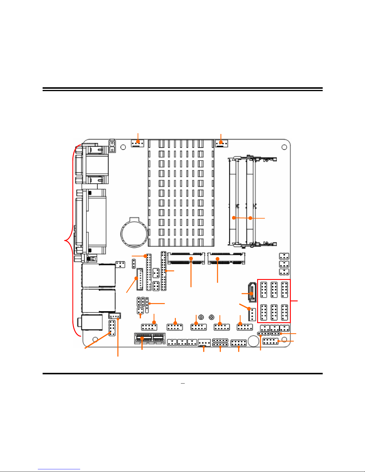
4
Motherboard Internal Diagram
PCIE x1
COM2
COM3
Serial Port Headers
(COM5/6/7//8/9/10)
SYSFAN1
CPUFAN
COM4
GPIO
JW_FP
SMBUS
SYSFAN2
LVDS
FP_USB3
FP_AUDIO
FP_USB1
FP_USB2
AMP_SPK
Mini-PCIe/M-SATA
Slot
Mini-PCIe Slot
SATA
SATAPWR
EDP
INVERTER
DDR4
SODIMM Slot
(SODIMM1/2)
JLAN_LED
*Rear IO
Connector
(Refer to Page-3)
PWRLED
JBUZZ
Page 10
5
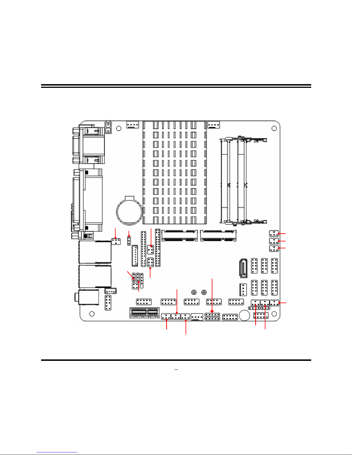
Jumper Positions:
JPCOM1
JPCOM2
JPCOM3
JPCOM4
JPCOM5
JPCOM6
JPCOM7
JPCOM8
JPCOM9
JPCOM10
JSYSFAN
JPLED
JRJ11_V
JBAT
JPLCD
JAT_COPEN
Page 11

6
Jumper Name Description
JPCOM1 COM1 Port Pin9 Function Select 4-pin Block
JPCOM2 COM2 Header Pin9 Function Select 4-pin Block
JPCOM3 COM3 Header Pin9 Function Select 4-pin Block
JPCOM4 COM4 Header Pin9 Function Select 4-pin Block
JPCOM5 COM5 Header Pin9 Function Select 4-pin Block
JPCOM6 COM6 Header Pin9 Function Select 4-pin Block
JPCOM7 COM7 Header Pin9 Function Select 4-pin Block
JPCOM8 COM8 Header Pin9 Function Select 4-pin Block
JPCOM9 COM9 Header Pin9 Function Select 4-pin Block
JPCOM10 COM10 Header Pin9 Function Select 4-pin Block
JAT_COPEN
Pin1&2&3: ATX/AT Mode Select
Pin 4&5 :
Case Open Message Display
Function Select
5-pin Block
JBAT
Pin 1&2:Clear CMOS RAM
Pin 3&4:Flash Override
Pin 5&6:POK Override
6-pin Block
JPLCD LVDS/eDP VCC 3.3V/5V/12V Select 4-pin Block
JPLED LVDS INVERTER/EDP Pane
Backlight 5V/12V Select
3-pin Block
JRJ11_V RJ-11 Cash Drawer Port
VCC 12 V/24V Select
3-pin Block
JSYSFAN SYSFAN1/SYSFAN2 Fan Speed Detect 3-pin Block
Page 12

7
Connectors
Connector
Name
DC_IN1 12V DC–in Power Jack Connector
VGA CRT VGA Port Connector
RJ11 RJ-11 Port Connector
PS2 PS/2 Keyboard & Mouse Connector
HDMI High-Definition Multimedia Interface Connector
LPT Parallel Port Connector
COM1 Serial Port Connector
USB1_LAN1/
USB2_LAN2
Top: RJ-45 LAN Port Connector x2
Middle: USB 3.0 Port Connector x2
Bottom: USB 3.0 Port Connector x2
AUDIO Top: Audio Line Out Port Connector
Bottom: Audio MIC In Connector
ATXPWR Internal 12V DC-in Power Connector
SATA SATAIII Port Connector
STATPWR SATA Power out Connector
CPUFAN CPU Fan Connector
SYSFAN1/SYSFAN2
System Fan Connector X 2
Page 13

8
Headers
Header Name Description
JW_FP Front Panel Header
(PWR LED/ HDD LED/
Power Button /Reset)
9-pin Block
PWRLED Power LED Header 3-pin Block
JBUZZ Buzzer Header 4-pin Block
FP_AUDIO Front Panel Audio Header 9-pin Block
AMP_SPK 3W Amplifier Header 4-pin Block
J_LAN_LED LAN Activity LED Header 4-pin Block
F_USB1/ F_USB2 USB 2.0 Header 9-pin Block
F_USB3 USB 2.0 Header 4-pin Block
COM2/3/4/5/67/8/9/10 Serial Port Header X9 9-pin Block
GPIO GPIO Header 10-pin Block
SMBUS SMBUS Header 5-pin Block
INVERTER LVDS INVERTER Header 8-pin Block
LVDS LVDS Header 30-pin Block
eDP eDP Header 29-pin Block
Page 14
9
Chapter 2
Hardware Installation
2-1 Jumper Setting
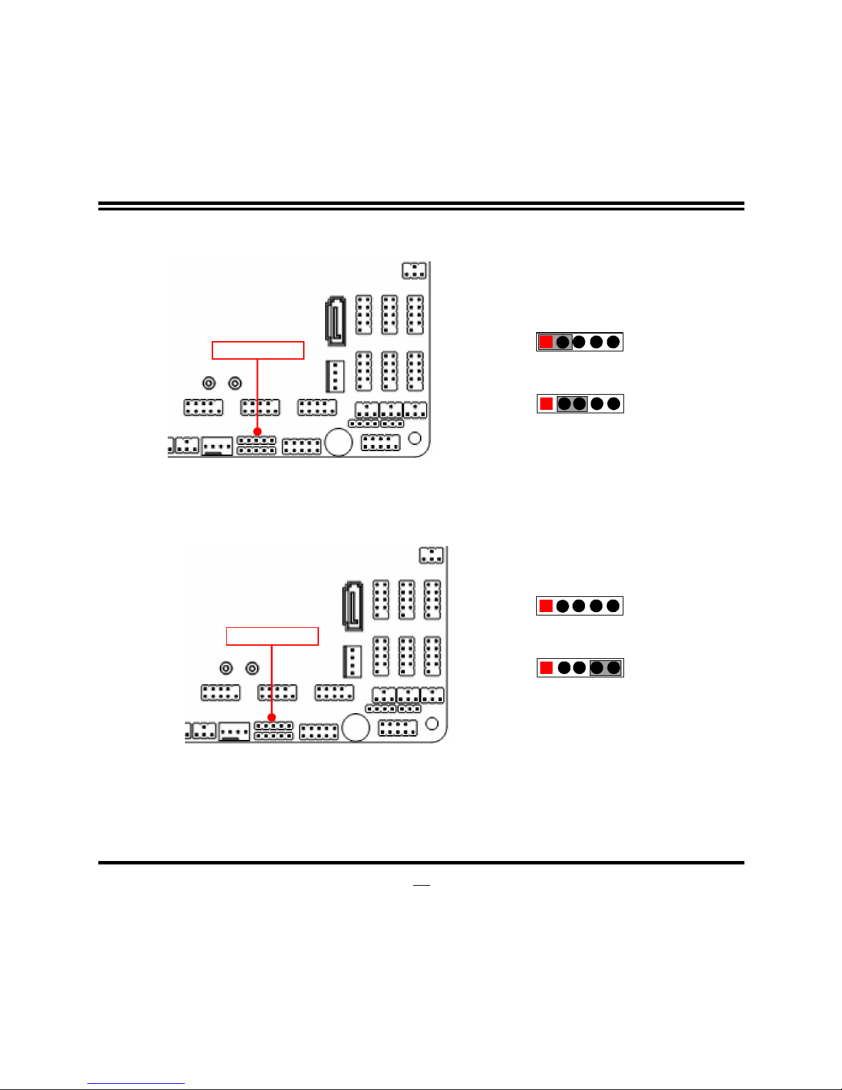
JPCOM1 (4-pin): COM1 Port Pin9 Function Select
JPCOM1→COM1 Port Pin9
4-6 Closed:
RI= 12V.
6 4 2
3-4 Closed:
RI= 5V;
2-4 Closed:
RI=RS232;
3
1
5
1
3
5
2 4
6
1 3
5
2 4 6
JPCOM2/3/4(4-pin): COM2/3/4 Header Pin9 Function Select
6
4
5
3
1
JPCOM2→COM2 Header Pin9
JPCOM3
→
COM3 Header Pin9
JPCOM4→COM4 Header Pin9
1 3
5
2
1 3 5
2
4
6
2 4
6
2-4 Closed:
RI=RS232;
3-4 Closed :
RI= 5V;
4-6 Closed:
RI= 12V.
JPCOM1
JPCOM2
JPCOM4
JPCOM3
Page 15
10
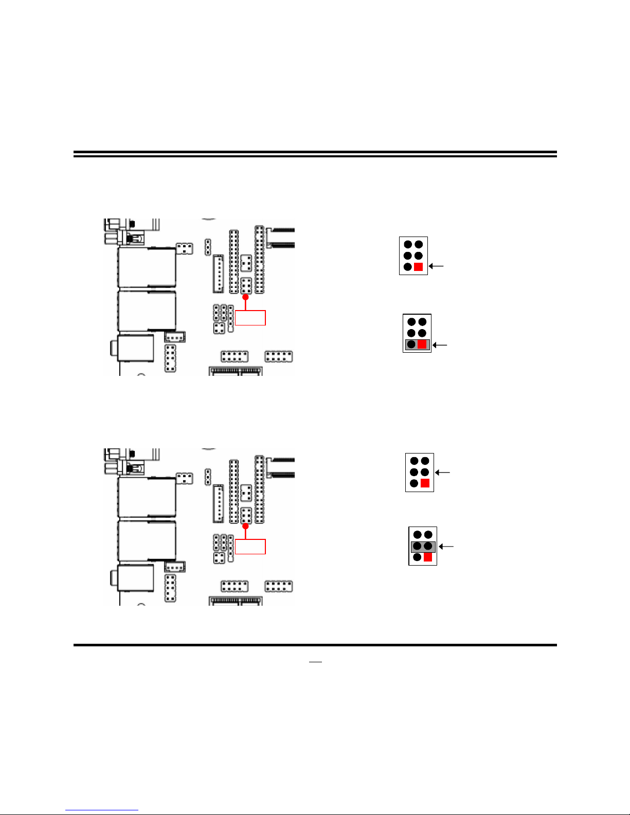
JPCOM5/6/7(4-pin): COM5/6/7 Header Pin9 Function Select
6
4
5
3
1
JCOMP5→COM5 Header Pin9
JCOMP6
→
COM6 Header Pin9
JCOMP7
→
COM7 Header Pin9
1 3
5
2
1 3 5
2
4
6
2 4
6
2-4 Closed:
RI=RS232;
3-4 Closed:
RI= 5V;
4-6 Closed :
RI= 12V.
JPCOM8/9/10(4-pin): COM8/9/10 Header Pin9 Function Select
6
4
5
3
1
JCOMP8→COM8 Header Pin9
JCOMP9→COM9 Header Pin9
JCOMP10→COM10 Header Pin9
1 3
5
2
1 3 5
2
4
6
2 4
6
2-4 Closed:
RI=RS232;
3-4 Closed:
RI= 5V;
4-6 Closed:
RI= 12V.
JPCOM5
JPCOM6
JPCOM7
JPCOM8
JPCOM9
J
PCOM10
Page 16
11
Pin 1&2&3 of JAT_COPEN (5-pin): ATX/AT Mode Select
Pin 1&2&3 of JAT_COPEN
→
ATX/AT Mode Select
1-2 Close: ATX Mode Selected(default);
1
3
2-3 Close: AT Mode Selected.
3
1
*ATX Mode Selected: Press power button to power on after power input ready;
AT Mode Selected: Directly power on as power input ready.
Pin 4 & 5 of JAT_COPEN (5-pin): Case Open Message Display Function Select
Pin 4&5 of JAT_COPEN
→
Case Open Function Select
4-5 Open:Normal (Default);
4 5
5
4
4-5 Close: Case Open
Function Selected (One Touch).
JAT_COPEN
JAT_COPEN
Page 17
12
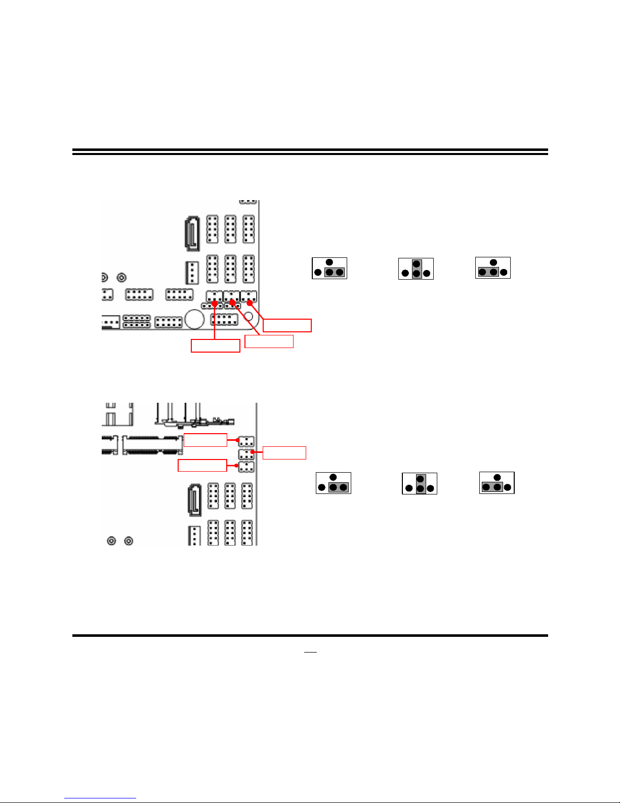
Pin 1&2 of JBAT (6-pin): Clear CMOS RAM Setting
Pin 1&2 of JBAT→ Clear CMOS Setting
Pin 1
1-2 Closed: Clear CMOS.
1-2 Open: Normal;
2
2
Pin 1
Pin 3&4 of JBAT (6-pin): Flash Override Function Slect
Pin 3
&
4 of JBAT
→
Flash Override
Pin 3
4
4
Pin 3
3-4 Open:Enable Security Measures
in the Flash Descriptor(Default);
3-4 Closed: Disable Security Measures
in the Flash Descriptor(Override).
JBAT
JBAT
Page 18
13
Pin 5&6 of JBAT (6-pin): POK Override Function Slect
Pin 5&6 of JBAT→ POK Override
Pin 5
6
6
Pin 5
5-6 Open:Normal;
5-6 Closed: POK Override.
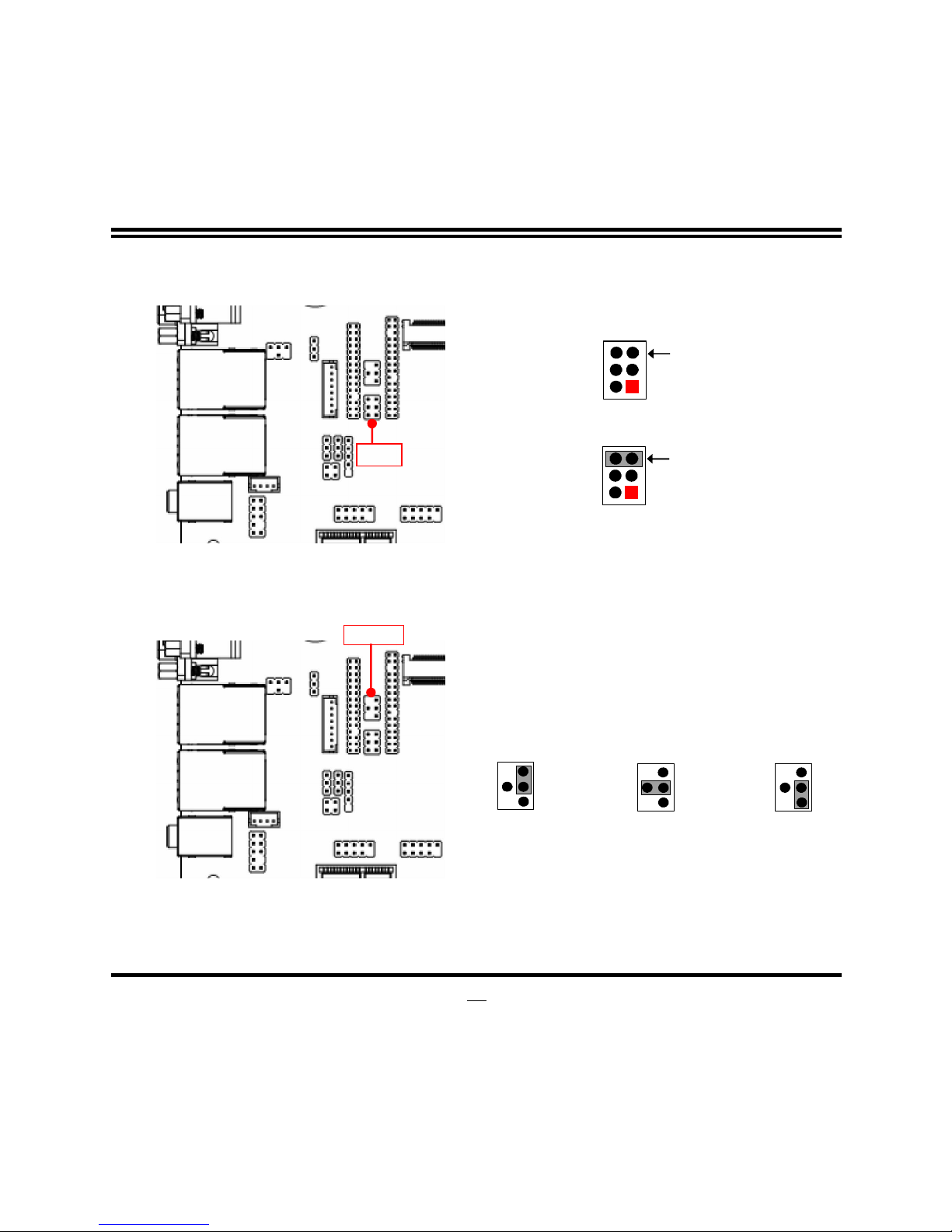
JPLCD (4-pin): LVDS/eDP LCD VCC 3.3V/5V/12V Select
JPLCD→LVDS/eDP LCD VCC
6
4
2
3
1
5
1
2
4
6
3
5
2
4
6
1
3
5
2-4 Closed:
VCC=3.3V
(Default);
3-4 Closed:
VCC= 5V;
4-6 Closed:
VCC= 12V.
JBAT
JPLCD
Page 19

14
JPLED (3-pin): LVDS INVERTER/EDP Panel Backlight VCC Select
2-3 Close: LVDS INVERTER/EDP Panel
Backlight 12V Selected.
JPLED→LVDS INVERTER/EDP Panel Backlight VCC
1-2 Close: LVDS INVERTER/EDP Panel
Backlight 5V Selected(Default);
1
3
3
1
JRJ11_V (3-pin): RJ-11 Cash Drawer Port VCC 12V/24V Select
JRJ11_V→RJ-11 Cash Drawer Port VCC
3
1
1
3
1-2 Close: RJ-11 Cash Drawer Port
Voltage=12V(Default);
2-3 Close: RJ-11 Cash Drawer Port
Voltage=24V.
JPLED
JRJ11_V
Page 20

15
JSYSFAN (3-pin): SYSFAN1/SYSFAN2 Speed Detect Select
1
3
3
1
JSYSFAN→SYSFAN1/2 Speed Detect Select
1-2 Close: SYSFAN1 Speed Detect Function Selected;
2-3 Closed: SYSFAN2 Speed Detect Function Selected.
2-2 Connectors and Headers
2-2-1 Connectors
(1) Rear I/O Connectors
Line-out Port
MIC Port
2*RJ-45
LAN Port
VGA Port
Parallel
Port
4* USB 3
.0 Port
Serial Port
HDMI Port
PS/2 KB & MS Port
12V DC-in
Power Jack
JSYSFAN
RJ-11
Cash Drawer Port
Page 21

16
Icon Name Function
DC 12V Power-out
Connector
For user to connect compatible power
adapter to provide power supply out.
VGA Port
To connect display device that support
VGA specification.
Parallel Port
Also called LPT connector. Mostly for user
to connect printer or scanner with parallel
interface.
RJ-11 Port
RJ-11for cash drawer I/F by GPIO control.
PS/2 Keyboard & Mouse
Connector
This combo port is for user to connect PS/2
mouse or keyboard device to the board.
HDMI Port
To connect display device that support
HDMI specification.
Serial Port
Mainly for user to connect external
MODEM or other devices that supports
Serial Communications Interface.
USB 3.0 Port
To
connect USB keyboard, mouse or other
devices compatible with USB specification.
USB 3.0 ports supports up to 5Gbps data
transfer rate.
RJ-45 LAN Port
This connector is standard RJ-45
LAN jack
for Network connection.
Line-Out Connector
For user to connect external speaker,
earphones, etc to transfer system audio
output.
Page 22

17
MIC Connector
For user to connect microphone.
(2) COM1 (9-pin Block): RS232/422/485 Port
COM1 port can function as RS232/422/485 port. In normal settings COM1 functions
as RS232 port. With compatible COM cable COM1 can function as RS422 or RS 485
port.
User also needs to go to BIOS to set ‘Transmission Mode Select’ for COM1 (refer to
Page 30) at first, before using specialized cable to connect different pins of this port.
For RS422 Mode
RS422 TX(B)
RS422 TX(A)
RS422 RX(A)
RS422 RX(B)
For RS485 Mode
RS485 D-(B)
RS485 D+(A)
(3) ATXPWR(2-pin Block): Internal 12V DC-in Power Connector
Pin1
Pin. Definition
1 GND
2 +12V DC_IN
Page 23

18
Warning!!
The board has a 12V DC-in power connector (DC_IN) in I/O back panel and an
internal ATX12V (ATXPWR) power connector. User can only connect one type of compatible
power supply to one of them to power the system.
(4) SATA (7-pin Block): SATAIII Port connector
SATA is a high-speed SATAIII port that supports 6GB/s transfer rate.
Pin No. Definition
1 GND
2 TXP
3 TXN
4 GND
5 RXN
6 RXP
7 GND
(5) SATAPW (4-pin): SATA Power Out Connector
Pin 1
+5V
GND
+12V
GND
SATA1
SATA
PW
Page 24

19
(6) SYSFAN1 (4-pin): SYSFAN1 Connector
SYSFAN1
Fan Speed
GND
Pin1
+12V Fan Power
Control
(7) SYSFAN2 (4-pin): SYSFAN2 Connector
SYSFAN
2
Fan Speed
GND
Pin1
+12V Fan Power
Control
SYSFAN1
SYSFAN2
Page 25

20
(8) CPUFAN (4-pin): CPUFAN Connector
CPUFAN
Fan Speed
GND
Pin1
+12V Fan Power
Control
2-2-2 Headers
(1) JW_FP (9-pin): Front Panel Header
HDDLED+
GND
PWRLED+
GND
PWRLED-
HDDLED- RSTSW
VCC
PWRBT
Pin 1
2
CPUFAN
JW_FP
Page 26

21
(2) PWRLED (3-pin): Power LED Header
PWRLED
-
Pin 1
PWRLED+
PWRLED
-
(3) JBUZZ (4-pin): Buzzer Header
Pin 1
BUZZER+
NC
NC
BUZZER
-
PWRLED
JBUZ
Z
Page 27

22
(4) FP_AUDIO (9-pin): Line-Out, MIC-In Header
This header connects to Front Panel Line-out, MIC-In connector with cable.
Line-Out, MIC Header
Pin 1
2
MIC-R
MIC-L
Lineout-R
Lineout-L
GND
NC
NC
KEY
NC
NC
(5) AMP_SPK (4-pin): 3W Amplifier Header
Pin No. Definition
1 L-
2 L+
3 R+
4 R-
Pin1
FP_AUDIO
AMP_SPK
Page 28

23
(6) JLAN _LED (4-pin): LAN2 RJ-45 LAN Header
2
Pin 1
USB1_LAN1 LAN ACT_LED+
USB1_LAN1 LAN ACT_LED-
USB2_LAN2 LAN ACT_LED+
USB2_LAN2 LAN ACT_LED-
(7) FP_USB1/ FP_USB1 (9-pin): USB 2.0 Port Header
Pin 1
VCC
-DATA
GND
+DATA
VCC
NC
-DATA
GND
+DATA
2
JLAN_LED
FP_USBSB2
FP_USBSB1
Page 29

24
(8) FP_USB3 (4-pin): USB 2.0 Port Header
Pin 1
VCC
GND
-DATA
+DATA
(9) COM2/3/4 (9-pin): Serial Port Headers
DCD
Pin1
Pin6
RXD
TXD
DTR
GND
DSR
RTS CTS
RI
FP_USBSB3
COM2
COM3
COM4
Page 30

25
(10) COM5/6/7/8/9/10 (9-pin): Serial Port Headers
DSR
RI
DCD
RXD
RTS
DTR
CTS TXD
GND
Pin1
6
(11) GPIO (10-pin): GPIO Header
GPIO_
20
GND
GPIO_22
GPIO_24
GPIO_26
GPIO_
21
GPIO_23
2
Pin 1
VCC
GPIO_
25
GPIO_
27
COM5
COM8
COM6
COM7
COM9
COM10
GPIO
Page 31

26
(12) SMBUS (5-Pin): SM BUS Header
SMBUS_CLK
Pin1
SMBUS_DATA
GND
3VSB
NC
(13) INVERTER (8-pin): LVDS Inverter Header
Pin1
Pin No. Definition
1 Backlight Enable
2 Backlight PWM
3 Backlight VCC
4 Backlight VCC
5 GND
6 GND
7 Backlight Up SW
8 Backlight Down SW
INVERTER
SUBUS
Page 32

27
(14) LVDS (30-Pin): 24-bit dual channel LVDS Header
Pin 1
Pin 2
Pin NO. Pin Define Pin NO. Pin Define
Pin 1 LVDSB_DATAN3 Pin 2 LVDSB_DATAP3
Pin 3 LVDS_CLKBN Pin 4 LVDS_CLKBP
Pin 5 LVDSB_DATAN2 Pin 6 LVDSB_DATAP2
Pin 7 LVDSB_DATAN1 Pin 8 LVDSB_DATAP1
Pin 9 LVDSB_DATAN0 Pin 10 LVDSB_DATAP0
Pin 11 NC Pin 12 NC
Pin 13 XX Pin 14 LVDS_DETECTPin 15 GND Pin 16 GND
Pin 17 LVDSA_DATAP3 Pin 18 LVDSA_DATAN3
Pin 19 LVDS_CLKAP Pin 20 LVDS_CLKAN
Pin 21 LVDSA_DATAP2 Pin 22 LVDSA_DATAN2
Pin 23 LVDSA_DATAP1 Pin 24 LVDSA_DATAN1
Pin 25 LVDSA_DATAP0 Pin 26 LVDSA_DATAN0
Pin 27 LCD_VCC Pin 28 XX
Pin 29 LCD_VCC Pin 30 LCD_VCC
Pin 31 GND Pin 32 GND
Note: EDP header shares function with LVDS header; i.e. only one can function at a time.
LVDS
Page 33

28
(15) EDP (29-Pin): EDP Header
Pin 1
Pin 2
Pin NO. Pin Define Pin NO. Pin Define
Pin 1 BKLT_PW Pin 2 BKLT_PW
Pin 3 BKLT_PW Pin 4 GND
Pin 5 GND Pin 6 NC
Pin 7 GND Pin 8 NC
Pin 9 EDP_VDD Pin 10 NC
Pin 11 EDP_VDD Pin 12 EDP Backlight PWM
Pin 13 GND Pin 14 GND
Pin 15 EDP Backlight Enable Pin 16 EDP_AUXP_C
Pin 17 EDP_HPD Pin 18 EDP_AUXNC
Pin 19 GND Pin 20 GND
Pin 21 EDP_LANE+3 Pin 22 EDP_LANE-3
Pin 23 EDP_LANE+2 Pin 24 EDP_LANE-2
Pin 25 GND Pin 26 GND
Pin 27 EDP_LANE+1 Pin 28 EDP_LANE-1
Pin 29 EDP_LANE+0 Pin 30 EDP_LANE-0
Note: EDP header shares function with LVDS header; i.e. only one can function at a time.
EDP
Page 34

29
Chapter 3
Introducing BIOS
Notice!
The BIOS options in this manual are for reference only. Different
configurations may lead to difference in BIOS screen and BIOS
screens in manuals are usually the first BIOS version when the board is
released and may be different from your purchased motherboard.
Users are welcome to download the latest BIOS version form our
official website.
The BIOS is a program located on a Flash Memory on the motherboard. This program
is a bridge between motherboard and operating system. When you start the computer,
the BIOS program will gain control. The BIOS first operates an auto-diagnostic test
called POST (power on self test) for all the necessary hardware, it detects the entire
hardware device and configures the parameters of the hardware synchronization.
Only when these tasks are completed done it gives up control of the computer to
operating system (OS). Since the BIOS is the only channel for hardware and software
to communicate, it is the key factor for system stability, and in ensuring that your
system performance as its best.
3-1 Entering Setup
Power on the computer and by pressing <Del> immediately allows you to enter Setup.
If the message disappears before your respond and you still wish to enter Setup,
restart the system to try again by turning it OFF then ON or pressing the “RESET”
button on the system case. You may also restart by simultaneously pressing <Ctrl>,
<Alt> and <Delete> keys. If you do not press the keys at the correct time and the
system does not boot, an error message will be displayed and you will again be asked
to
Press
<Del>
to enter Setup; press <
F7
> for Pop Menu.
Page 35

30
3-2 BIOS Menu Screen
The following diagram show a general BIOS menu screen:
BIOS Menu Screen
3-3 Function Keys
In the above BIOS Setup main menu of, you can see several options. We will explain
these options step by step in the following pages of this chapter, but let us first see a
short description of the function keys you may use here:
Press (left, right) to select screen;
Press (up, down) to choose, in the main menu, the option you want to confirm
or to modify.
Menu Bar
Menu Items
Current Setting Value
Function Keys
General Help Items
Page 36

31
Press
<Enter>
to select.
Press
<+>/<–>
keys when you want to modify the BIOS parameters for the active
option.
[F1]:
General help.
[F2]:
Previous value.
[F3]:
Optimized defaults.
[F4]:
Save & Exit.
Press
<Esc>
to exit from the BIOS Setup.
3-4 Getting Help
Main Menu
The on-line description of the highlighted setup function is displayed at the top right
corner the screen.
Status Page Setup Menu/Option Page Setup Menu
Press
[F1]
to pop up a small help window that describes the appropriate keys to use
and the possible selections for the highlighted item. To exit the Help Window, press
<
Esc
>.
3-5 Menu Bars
There are six menu bars on top of BIOS screen:
Main To change system basic configuration
Advanced To change system advanced configuration
Chipset To change chipset configuration
Security Password settings
Boot To change boot settings
Save & Exit Save setting, loading and exit options.
User can press the right or left arrow key on the keyboard to switch from menu bar.
The selected one is highlighted.
Page 37

32
3-6 Main Menu
Main menu screen includes some basic system information. Highlight the item and
then use the <+> or <-> and numerical keyboard keys to select the value you want in
each item.
System Date
Set the date. Please use [Tab] to switch between data elements.
System Time
Set the time. Please use [Tab] to switch between time elements.
Page 38

33
3-7 Advanced Menu
CPU Configuration
Press [Enter] to view current CPU configuration and make settings for the following
sub-items:
Intel Virtualization Technology
The optional settings: [Disabled]; [Enabled].
When enabled, a VMM can utilize the additional hardware capabilities provided by
Vanderpool Technology.
Hardware Prefetcher
The optional settings are: [Disabled]; [Enabled].
Use this item to enable the Mid Level Cache (L2) streamer prefetcher.
Adjacent Cache Line Prefetch
The optional settings are: [Disabled]; [Enabled].
Use this item to enable Mid Level Cache (L2) prefetching of adjacent cache lines.
Page 39

34
Intel(R) SpeedStep(tm)
Use this item to enable or disable Intel SpeedStep.When set as [Enabled], it allows
more than two frequency ranges to be supported.
The optional settings: [Disabled]; [Enabled].
CPU C States
Use this item to enable or disable CPU Power Management. When set as
[Enabled], it allows CPU to go to C states when it’s not 100% utilized.
The optional settings: [Disabled]; [Enabled].
Package C State Limit
Use this item to select maximum package C State Limit setting.
The optional settings: [C0/C1]; [C2]; [C3]; [C6]; [C7]; [C7S]; [C8]; [C9]; [C10];
[Cpu Default]; [Auto].
SATA Configuration
Press [Enter] to make settings for the following sub-items:
SATA Controller(s)
The optional settings are: [Enabled]; [Disabled].
When set as [Enabled], the following items shall appear:
SATA Mode Selection
This item determines how SATA controller(s) operate.
The default setting is: [AHCI].
mSATA
Port
The optional settings are: [Enabled]; [Disabled].
SATA
Port
The optional settings are: [Enabled]; [Disabled].
Hot Plug
The optional settings are: [Enabled]; [Disabled].
PCH-FW Configuration
Press [Enter] to view ME information and make settings in the following sub-items:
Page 40

35
TPM Device Selection
Use this item to select TPM device.
The optional settings are: [dTPM]; [PTT]. .
▶
Firmware Update Configuration
Press [Enter] to make settings for ‘ME FW Image RE-Flash’.
▶
ME FW Image Re-Flash
Use this item to enable or disable ME FW Image Re-Flash function.
The optional settings: [Disabled]; [Enabled].
* In the case that user needs to update ME firmware, user should set ‘ME FW
Image Re-Flash’ as [Enabled], save the settings and exit. The system will turn off
and reboot after 4 seconds. If the user goes to BIOS screen again will find this item
is set again as [Disabled], but user can still re-flash to update firmware next time.
► Trusted Computing
Press [Enter] to enable or disable ‘
Security Device Support
’.
Security Device Support
Use this item to enable or disable BIOS support for security device.
The optional settings: [Disabled]; [Enabled].
ACPI Settings
Press [Enter] to make settings for the following sub-item:
ACPI Sleep State
Use this item to select the highest ACPI sleep state the system will enter when the
suspend button is pressed.
The optional settings are: [Suspend Disabled]; [S3 (Suspend to RAM)].
► Wake-up Function Settings
Press [Enter] to make settings for the following sub-items:
Wake-up System with Fixed Time
Use this item to enable or disable system wake on alarm event.
The optional settings: [Disabled]; [Enabled].
When set as [Enabled], system will wake on the hour/min/sec specified.
Wake-up System with Dynamic Time
Page 41

36
Use this item to enable or disable system wake on alarm event.
System will wake on the current time + Increase minutes.
The optional settings: [Disabled]; [Enabled].
When set as [Enabled], system will wake on the current time + increased
minute(s).
PS2 KB/MS Wake-up
The optional settings: [Enabled]; [Disabled].
Use this item to enable or disable PS2 KB/MS wake-up from S3/S4/S5.
* Note: This function is supported when ‘ERP Support’ is set as [Disabled].
USB S3/S4 Wake-up
Use this item to enable or disable USB S3/S4 wakeup. This function is only
supported when ERP function is disabled.
* Note: This function is supported when ‘ERP Support’ is set as [Disabled].
USB S5 Power
Use this item to enable or disable USB power after power shutdown.
*This function is supported when ‘ERP Support’ is set as [Disabled].
Super I/O Configuration
Press [Enter] to make settings for the following sub-items:
Super IO Configuration
ERP Support
The optional settings: [Disabled]; [Auto].
This item should be set as [Disabled] if you wish to have all active wake-up
functions.
► Serial Port 1 Configuration
Press [Enter] to make settings for the following items:
Serial Port
Use this item to enable or disable serial port (COM).
Change Settings
Use this item to select an optimal setting for super IO device.
The optional settings are: [IO=3F8h; IRQ=4]; [IO=3F8h; IRQ=3,4,5,6,7,
Page 42

37
9,10,11,12]; [IO=2F8h; IRQ=3,4,5,6,7, 9,10,11,12]; [IO=3E8h; IRQ=3,4,5,6,7,
9,10,11,12]; [IO=2E8h; IRQ=3,4,5,6,7,9,10,11,12].
Transmission Mode Select
The optional settings are: [RS422]; [RS232]; [RS485].
Mode Speed Select
The optional settings are: [RS232/RS422/RS485=250kbps]; [RS232=1Mbps,
RS422/RS485=10Mbps].
Serial Port FIF0 Mode
The optional settings are: [16-Byte FIF0]; [32-Byte FIF0]; [64-Byte FIF0]; [128-Byte
FIF0].
► Serial Port 2 Configuration/ Serial Port 3 Configuration/Serial Port 4
Configuration/ Serial Port 5 Configuration/ Serial Port 6 Configuration
Press [Enter] to make settings for the following sub-items:
Serial Port
Use this item to enable or disable serial port (COM).
Change Settings
Use this item to select an optimal setting for super IO device.
The optional settings are: [IO=2F8h; IRQ=3]; [IO=3F8h; IRQ=3,4,5,6,7,
9,10,11,12]; [IO=2F8h; IRQ=3,4,5,6,7, 9,10,11,12]; [IO=3E8h; IRQ=3,4,5,6,7,
9,10,11,12]; [IO=2E8h; IRQ=3,4,5,6,7, 9,10,11,12] for ‘Serial Port 2
Configuration’.
The optional settings are: [IO=3E8h; IRQ=10]; [IO=3F8h; IRQ=3,4,5,6,7,
9,10,11,12]; [IO=2F8h; IRQ=3,4,5,6,7, 9,10,11,12]; [IO=3E8h; IRQ=3,4,5,6,7,
9,10,11,12]; [IO=2E8h; IRQ=3,4,5,6,7, 9,10,11,12] ; [IO=3E0h; IRQ=3,4,5,6,7,
9,10,11,12]; [IO=2E0h; IRQ=3,4,5,6,7, 9,10,11,12] for ‘Serial Port 3
Configuration’.
The optional settings are: [IO=2E8h; IRQ=10]; [IO=3F8h; IRQ=3,4,5,6,7,
9,10,11,12]; [IO=2F8h; IRQ=3,4,5,6,7, 9,10,11,12]; [IO=3E8h; IRQ=3,4,5,6,7,
9,10,11,12]; [IO=2E8h; IRQ=3,4,5,6,7, 9,10,11,12] ; [IO=3E0h; IRQ=3,4,5,6,7,
9,10,11,12]; [IO=2E0h; IRQ=3,4,5,6,7, 9,10,11,12] for ‘Serial Port 4
Configuration’.
Page 43

38
The optional settings are: [IO=3E0h; IRQ=10]; [IO=3F8h; IRQ=3,4,5,6,7,
9,10,11,12]; [IO=2F8h; IRQ=3,4,5,6,7, 9,10,11,12]; [IO=3E8h; IRQ=3,4,5,6,7,
9,10,11,12]; [IO=2E8h; IRQ=3,4,5,6,7, 9,10,11,12] ; [IO=3E0h; IRQ=3,4,5,6,7,
9,10,11,12]; [IO=2E0h; IRQ=3,4,5,6,7, 9,10,11,12] for ‘Serial Port 5
Configuration’.
The optional settings are: [IO=2E0h; IRQ=10]; [IO=3F8h; IRQ=3,4,5,6,7,
9,10,11,12]; [IO=2F8h; IRQ=3,4,5,6,7, 9,10,11,12]; [IO=3E8h; IRQ=3,4,5,6,7,
9,10,11,12]; [IO=2E8h; IRQ=3,4,5,6,7, 9,10,11,12] ; [IO=3E0h; IRQ=3,4,5,6,7,
9,10,11,12]; [IO=2E0h; IRQ=3,4,5,6,7, 9,10,11,12] for ‘Serial Port 6
Configuration’.
Parallel Port Configuration
Press [Enter] to make settings for the following items:
Parallel Port Configuration
Parallel Port
Use this item to enable or disable serial port (LPT/LPTE).
The optional settings are: [Disabled]; [Enabled].
Change Settings
Use this item to select an optimal setting for super IO device.
The optional settings are: [Auto]; [IO=378h; IRQ=7];
[IO=378h; IRQ=5,6,7,9,10,11,12]; [IO=278h; IRQ=5,6,7,9,10,11,12];
[IO=3BCh; IRQ=5,6,7,9,10,11,12];[IO=378h];[IO=278h]; [IO=3BCh].
Device Mode
The optional settings are: [STD Printer Mode]; [SPP Mode]; [EPP-1.9 and SPP
Mode]; [EPP-1.7 and SPP Mode]; [ECP Mode]; [ECP and EPP 1.9 Mode]; [ECP
and EPP 1.7 Mode].
WatchDog Reset Timer
Use this item to enable or disable WDT reset function. When set as [Enabled], the
following sub-items shall appear:
WatchDog Reset Timer Value
User can set a value in the range of [4] to [255].
Page 44

39
WatchDog Reset Timer Unit
The optional settings are: [Sec.]; [Min.].
WatchDog Wake-up Timer in ERP
This item support WDT wake-up while ‘ERP Support’ is set as [Auto].
The optional settings: [Disabled]; [Enabled].
When set as [Enabled], the following sub-items shall appear:
WatchDog Wake-up Timer Value in ERP
User can select a value in the range of [10] to [4095] seconds when ‘WatchDog
Reset Timer Unit’ set as [Sec]; or in the range of [1] to [4095] minutes when
‘WatchDog Reset Timer Unit ’ set as [Min].
WatchDog Reset Timer Unit
The optional settings are: [Sec.]; [Min.].
ATX Power Emulate AT Power
This item support Emulate AT power function, MB power On/Off control by power
supply. Use needs to select ‘AT or ATX Mode’ on MB jumper at first (refer to Page-
11: Pin 1&2&3 of JAT_COPEN jumper for ATX Mode & AT Mode Select).
Case Open Detect
Use this item to detect case has already open or not, show message in POST.
PS2 KB/MS Connect
The optional settings are: [Keyboard First]; [Mouse First].
PC Health Status
Press [Enter] to view current hardware health status, set shutdown temperature, or
make further settings in ‘SmartFan Configuration’.
SmartFan Configuration
Press [Enter] to make settings for SmartFAN Configuration:
CPUFAN/SYSFAN1Smart Mode
The optional settings are: [Disabled]; [Enabled].
When set as [Enabled], the following sub-items shall appear:
CPUFAN/SYSFAN1 Full-Speed Temperature
Page 45

40
Use this item to set CPUFAN full speed temperature. Fan will run at full speed
when above the pre-set temperature.
CPUFAN/SYSFAN1 Full-Speed Duty
Use this item to set CPUFAN full speed duty. Fan will run at full speed when
above the pre-set duty.
CPUFAN/SYSFAN1 Idle-Speed Temperature
Use this item to set CPUFAN idle speed temperature. Fan will run at idle speed
when below the pre-set temperature.
CPUFAN/SYSFAN1 Idle-Speed Duty
Use this item to set CPUFAN idle speed duty. Fan will run at idle speed when
below the pre-set duty.
SYSFAN1 Type
The optional settings are: [4-Pin]; [3-Pin].
Shutdown Temperature
Use this item to select system shutdown temperature.
The optional settings are: [Disabled]; [70°C/156°F]; [75°C/164°F]; [80°C/172°F];
[85°C/180°F]; [90°C/188°F].
Second IO Configuration
Press [Enter] to make settings for the following sub-items:
Second IO Configuration
► Serial Port 7 Configuration/ Serial Port 8 Configuration/Serial Port 9
Configuration/ Serial Port 10 Configuration
Press [Enter] to make settings for the following sub-items:
Serial Port
Use this item to enable or disable serial port (COM).
Change Settings
Use this item to select an optimal setting for super IO device.
The optional settings are: [IO=240h; IRQ=11]; [IO=240h; IRQ=5, 10,11]; ;
[IO=248h; IRQ=5, 10,11]; [IO=250h; IRQ=5, 10,11]; ; [IO=258h; IRQ=5, 10,11] for
‘Serial Port 7 Configuration’.
Page 46

41
The optional settings are: [IO=248h; IRQ=11]; [IO=240h; IRQ=5, 10,11]; ;
[IO=248h; IRQ=5, 10,11]; [IO=250h; IRQ=5, 10,11]; ; [IO=258h; IRQ=5, 10,11] for
‘Serial Port 8 Configuration’.
The optional settings are: [IO=250h; IRQ=11]; [IO=240h; IRQ=5, 10,11]; ;
[IO=248h; IRQ=5, 10,11]; ; [IO=250h; IRQ=5, 10,11]; ; [IO=258h; IRQ=5, 10,11] for
‘Serial Port 9 Configuration’.
The optional settings are: [IO=258h; IRQ=11]; [IO=240h; IRQ=5, 10,11]; ;
[IO=248h; IRQ=5, 10,11]; ; [IO=250h; IRQ=5, 10,11]; ; [IO=258h; IRQ=5, 10,11] for
‘Serial Port 10 Configuration’.
Serial Port Console Redirection
Press [Enter] to make settings for serial port redirection settings:
COM1
Console Redirection
The optional settings are: [Disabled]; [Enabled].
When set as [Enabled], user can make further settings in:
Console Redirection Settings
The settings specify how the host computer and the remote computer (which the
user is using) will exchange data. Both computers should have the same or
compatible settings.
Press [Enter] to make settings for the following sub-items.
Terminal Type
The optional settings are: [VT100]; [VT100+]; [VT-UTF8]; [ANSI].
Bits per second
The optional settings are: [9600]; [19200]; [38400]; [57600]; [115200].
Data Bits
The optional settings are: [7]; [8].
Parity
The optional settings are: [None]; [Even]; [Odd]; [Mark]; [Space].
Stop Bits
The optional settings are: [1]; [2].
Flow Control
Page 47

42
The optional settings are: [None]; [Hardware RTS/CTS].
VT-UTF8 Combo Key Support
The optional settings are: [Disabled]; [Enabled].
Recorder Mode
The optional settings are: [Disabled]; [Enabled].
Resolution 100x31
Use this item to disable or enable extended terminal resolution.
The optional settings are: [Disabled]; [Enabled].
Legacy OS Redirection Resolution
The optional settings are: [80x24]; [80x25].
Putty Keypad
The optional settings are: [VT100]; [LINUX]; [XTERMR6]; [SCO]; [ESCN];
[VT400].
Redirection After BIOS POST
The optional settings are: [Always Enable]; [BootLoader].
Serial Port for Out-of-Band Management/
Windows Emergency Management Services (EMS)
Console Redirection
The optional settings are: [Enabled]; [Disabled].
When set as [Enabled], user can make further settings in ‘Console Redirection
Settings’:
Console Redirection Settings
The settings specify how the host computer and the remote computer (which the
user is using) will exchange data. Both computers should have the same or
compatible settings.
Press [Enter] to make settings for the following sub-items.
Out-of-Band Mgmt Port
The optional settings are: [COM1]; [COM1(Pci Bu0, Dev0, Func0) (Disabled)].
*This item may or may not show up, depending on different configuration.
Terminal Type
The optional settings are: [VT100]; [VT100+]; [VT-UTF8]; [ANSI].
Page 48

43
Bits per second
The optional settings are: [9600]; [19200]; [57600]; [115200].
Flow Control
The optional settings are: [None]; [Hardware RTS/CTS]; [Software Xon/Xoff].
Data Bits
The default setting is: [8].
*This item may or may not show up, depending on different configuration.
Parity
The default setting is: [None].
*This item may or may not show up, depending on different configuration.
Stop Bits
The default setting is: [1].
*This item may or may not show up, depending on different configuration.
Network Stack Configuration
Press [Enter] to go to ‘Network Stack’ screen to enable or disable UEFI Network
Stack.
Network Stack
The optional settings are: [Enabled]; [Disabled].
When set as [Enabled], the following sub-items shall appear:
Ipv4 PXE Support
The optional settings are: [Disabled]; [Enabled].
Use this item to enable Ipv4 PXE Boot Support. When set as [Disabled], Ipv4 boot
option will not be created.
Ipv4 HTTP Support
The optional settings are: [Disabled]; [Enabled].
Use this item to enable Ipv4 HTTP Boot Support. When set as [Disabled], Ipv4
HTTP boot option will not be created.
Ipv6 PXE Support
The optional settings are: [Disabled]; [Enabled].
Use this item to enable Ipv6 PXE Boot Support. When set as [Disabled], Ipv6 boot
optional will not be created.
Page 49

44
Ipv6 HTTP Support
The optional settings are: [Disabled]; [Enabled].
Use this item to enable Ipv6 HTTP Boot Support. When set as [Disabled], Ipv6
HTTP boot option will not be created.
PXE boot wait time
Use this item to set wait time to press [ESC] key to abort the PXE boot.
Media Detect Count
Use this item to set number of times presence of media will be checked.
The optional settings range from [1] to [50].
CSM Configuration
Press [Enter] to make settings for the following sub-items:
Option ROM execution
Network
This item controls the execution of UEFI and Legacy PXE OpROM.
The optional settings are: [Do Not Launch]; [Legacy only].
Storage
This option controls the execution of UEFI and Legacy Storage OpROM.
The optional settings are: [Do Not Launch]; [UEFI only]; [Legacy only].
Other PCI Devices
This item determines OpROM execution policy for devices other than Network,
storage or video.
The optional settings are: [Do Not Launch]; [UEFI only]; [Legacy only].
USB Configuration
Press [Enter] to make settings for the following sub-items:
USB Configuration
Legacy USB Support
The optional settings are: [Enabled]; [Disabled]; [Auto].
[Enabled]: To enable legacy USB support.
[Disabled]: To keep USB devices available only for EFI specification,
[Auto]: To disable legacy support if no USB devices are connected.
XHCI Hand-off
Page 50

45
This is a workaround for OSes without XHCI hand-off support. The XHCI
ownership change should be claimed by XHCI driver.
The optional settings are: [Enabled]; [Disabled].
USB Mass Storage Driver Support
The optional settings are: [Disabled]; [Enabled].
USB hardware delay and time-outs:
USB Transfer time-out
Use this item to set the time-out value for control, bulk, and interrupt transfers.
The optional settings are: [1 sec]; [5 sec]; [10 sec]; [20 sec].
Device reset time-out
Use this item to set USB mass storage device start unit command time-out.
The optional settings are: [10 sec]; [20 sec]; [30 sec]; [40 sec].
Device power-up delay
Use this item to set maximum time the device will take before it properly reports
itself to the host controller. ‘Auto’ uses default value: for a root port it is 100 ms, for
a hub port the delay is taken from hub descriptor.
The optional settings: [Auto]; [Manual].
Select [Manual] you can set value for the following sub-item: ‘Device Power-up
Delay in Seconds’.
Device Power-up Delay in Seconds
The delay range is from [1] to [40] seconds, in one second increments.
Realtek PCIe GBE Family Controller (MAC:XX:XX:XX:XX:XX:XX)/ Realtek
PCIe GBE Family Controller (MAC:XX:XX:XX:XX:XX:XX)
This item gives Intel gigabit ethernet controller basic driver information.
Page 51

46
3-8 Chipset Menu
► System Agent (SA) Configuration
Press [Enter] to make settings for the following sub-items:
VT-d
The optional settings are: [Disabled]; [Enabled].
► Graphics Configuration
Press [Enter] to make further settings for Graphics Configuration.
GTT Size
The optional settings are: [2MB]; [4MB]; [8MB].
Aperture Size
The optional settings are: [128MB]; [256MB]; [512MB]; [1024MB].
DVMT Pre-Allocated
Use this item to select DVMT 5.0 pre-allocated (fixed) graphics memory size used
by the internal graphics device.
Page 52

47
The optional settings are: [32M]; [64M]; [96M]; [128M]; [160M]; [192M]; [224M];
[256M]; [288M]; [320M]; [352M]; [384M]; [416M]; [448M]; [480M]; [512M]; [1024M];
[1536M]; [2048M]; [4M]; [8M]; [12M]; [16M]; [20M]; [24M]; [28M]; [32M/F7];
[36M]; [40M]; [44M]; [48M]; [52M]; [56M]; [60M].
DVMT Total Gfx Mem
Use this item to select DVMT 5.0 total graphics memory size used by the internal
graphics device.
The optional settings are: [128M]; [256M]; [MAX].
Primary IGFX Boot Display
Use this item to select Video Device which will be activated during POST. This has
no effect if external graphics present. Secondary boot display selection will appear
based on selection. BGA modes will be supported only on primary display.
The optional settings are: [VBIOS Default]; [HDMI]; [CRT]; [eDP/LVDS].
* Note: When set as [HDMI], [CRT], or [eDP/LVDS], user can make further settings
in‘Second IGFX Boot Display’.
Second IGFX Boot Display
Use this item to select second IGFX boot device..
The optional settings are: [Disabled]; [HDMI]; [CRT].
Active LFP
The optional settings are: [eDP]; [LVDS].
*When set as [LVDS], the following sub-items shall appear:
Backlight Control
Use this item to select Back Light Control setting.
The optional settings are: [PWM inverted]; [PWM Normal].
Panel Type
Use this item to select Panel Type.
The optional settings are: [800x480 18bit Single]; [800x600 18bit Single];
[800x600 24bit Single]; [1024x600 18bit Single]; [1024x768 18bit Single];
[1024x768 24bit Single]; [1280x768 24bit Single]; [1280x800 18bit Single];
[1280x800 24bit Single]; [1366x768 18bit Single]; [1366x768 24bit Single];
[1440x900 18bit Dual]; [1440x900 24bit Dual]; [1280x1024 24bit Dual];
Page 53

48
[1680x1050 24bit Dual]; [1920x1080 24bit Dual].
LVDS FW Write Protect
Use this item to select LVDS FW Update/Protect.
The optional settings are: [Disabled]; [Enabled].
► Memory Configuration
Press [Enter] to view brief information for the working memory module.
► PCH-IO Configuration
Press [Enter] to make settings for the following sub-items:
USB Controller
Use this item to enable or disable this USB physical connector (physical port).
Once disabled, any USB devices plugged into this connector will not be detected
by BIOS or OS.
The optional settings are: [Disabled]; [Enabled].
HD Audio
Use this item to control the detection of the HD Audio device.
The optional settings are: [Disabled]; [Enabled]; [Auto].
[Disabled]: HDA will be unconditionally disabled;
[Enabled]: HDA will be unconditionally enabled;
[Auto]: HAD will be enabled if present, or disabled otherwise.
Onboard Lan1 Controller/ Onboard Lan2 Controller
Use this item to enable or disable device or controller.
The optional settings are: [Enabled]; [Disabled].
PCI-E Slot
Use this item to enable or disable device or controller.
The optional settings are: [Enabled]; [Disabled].
Speed
The optional settings are: [Auto]; [Gen1]; [Gen2]; [Gen3].
MPE Slot
Use this item to enable or disable device or controller.
Page 54

49
The optional settings are: [Disabled]; [Enabled].
Speed
The optional settings are: [Auto]; [Gen1]; [Gen2]; [Gen3].
MMPE Slot
Use this item to enable or disable device or controller.
The optional settings are: [Disabled]; [Enabled].
Speed
The optional settings are: [Auto]; [Gen1]; [Gen2]; [Gen3].
System State after Power Failure
Use this item to specify what state to go to when power re-applied after a power
failure (G3 state).
The optional settings are: [Always On]; [Always Off]; [Former State].
3-9 Security Menu
Page 55

50
Security menu allow users to change administrator password and user password
settings.
Administrator Password
Press [Enter] to create new administrator password. Press again to confirm the new
administrator password.
User Password
Press [Enter] to create new user password. Press again to confirm the new user
password.
3-10 Boot Menu
Boot Configuration
Setup Prompt Timeout
Use this item to set number of seconds to wait for setup activation key.
Page 56

51
Bootup Numlock State
Use this item to select keyboard numlock state.
The optional settings are: [On]; [Off].
Quiet Boot
The optional settings are: [Disabled]; [Enabled].
Boot Option Priorities
Boot Option #1/…
The optional settings are: [UEFI: Built-in EFI Shell]; [Disabled].
UEFI Boot
The optional settings are: [Disabled]; [Enabled].
[Enabled]: To enable all UEFI boot options.
[Disabled]:To disabled all UEFI boot options.
3-11 Save & Exit Menu
Page 57

52
Save Options
Save Changes and Reset
This item allows user to reset the system after saving the changes.
Discard Changes and Reset
This item allows user to reset the system without saving any changes.
Default Options
Restore Defaults
Use this item to restore /load default values for all the setup options.
Save as User Defaults
Use this item to save the changes done so far as user defaults.
Restore User Defaults
Use this item to restore defaults to all the setup options.
Boot Override
UEFT: Built-in EFI Shell
Launch Internal EFI shell application (shell.efi).
Lauch EFI Shell from filesystem device
Use this item to launch EFI shell application (shell.efi) from one of the available
filesystem device.
 Loading...