

JETWAY 618TAS, 618TAF User Manual

618TAS/618TAF
USER'S MANUAL
M/B For Socket 370 Pentium III Processor
NO. G03-618TAS3A
Release date: July 2002
Trademark:
* Specifications and Information contained in this documentation are furnished for information use only, and are
subject to change at any time without notice, and should not be construed as a commitment by manufacturer.

i
USER’S NOTICE ............................................................................. ii
MANUAL REVISION INFORMATION ............................................. 1
THERMAL SOLUTIONS ................................................................... 1
CHAPTER 1 INTRODUCTION OF MOTHERBOARD
1-1 FEATURE OF MOTHERBOARD............................................................... 2
1-2 SPECIFICATION .......................................................................................... 3
1-3 PERFORMANCE LIST ................................................................................ 4
1-3-1 618TAF ...........................................................................................................4
1-3-2 618TAS............................................................................................................
5
1-4 LAYOUT DIAGRAM & JUMPER SETTING........................................... 6
CHAPTER 2 HARDWARE INSTALLATION
2-1 HARDWARE INSTALLATION STEPS..................................................... 8
2-2 CHECKING MOTHERBAORD'S JUMPER SETTING .......................... 8
2-3 INSTALL CPU ............................................................................................... 10
2-3-1 GLOSSARY
........................................................................................... 10
2-3-2 SETTING CPU BUS CLOCK & MEMORY CLOCK JUMPER
........... 11
2-3-3 INSTALL CPU...............................................................................................12
2-3-4 OVERCLOCK RUNNING ...........................................................................
13
2-4 INSTALL MEMORY .................................................................................... 14
2-5 EXPANSION CARDS.................................................................................... 15
2-5-1 PROCEDURE FOR EXPANSION CARD INSTALLATION ..................15
2-5-2 ASSIGNING IRQ FOR EXPANSION CARD ............................................
15
2-5-3 INTERRUPT REQUEST TABLE FOR THIS MOTHERBOARD..........
16
2-5-4 AIMM/AGP SLOT ........................................................................................
16
2-6 CONNECTORS, HEADERS ........................................................................ 17
2-6-1 CONNECTORS.................................................................................. 17
2-6-2 HEADERS........................................................................................... 19
2-7 STARTING UP YOUR COMPUTER.......................................................... 23
CHAPTER 3 INTRODUCING BIOS
3-1 ENTERING SETUP....................................................................................... 24
3-2 GETTING HELP ........................................................................................... 25
3-3 THE MAIN MENU ........................................................................................ 25
3-4 STANDARD CMOS FEATURES ................................................................ 27
3-5 ADVANCED BIOS FEATURES .................................................................. 28
3-6 ADVANCED CHIPSET FEATURES .......................................................... 30
3-6-1 SDRAM TIMING SETTING........................................................................32
3-7 INTEGRATED PERIPHERALS.................................................................. 33
3-7-1 ON-CHIP IDE FUNCTION..........................................................................34
3-7-2 ON-CHIP SIO FUNCTION ..........................................................................
35
3-7-3 ON-CHIP DEVICE FUNCTION .................................................................
36
3-8 POWER MANAGEMENT SETUP.............................................................. 37
TABLE OF CONTENT

ii
3-9 PNP/PCI CONFIGURATION SETUP ........................................................ 39
3-10 PC HEALTH STATUS................................................................................. 40
3-11 MISCELLANEOUS CONTROL ................................................................ 41
3-12 LOAD STANDARD/OPTIMIZED DEFAULTS ....................................... 42
3-13 SET SUPERVISOR/USER PASSWORD................................................... 42
CHAPTER 4 DRIVER & FREE PROGRAM INSTALLATION
MAGIC INSTALL SUPPORTS WINDOWS 95/98/98SE/NT4.0/2000 ............. 43
4-1 INF
INSTALL INTEL 815 CHIPSET SYSTEM DRIVER
.............................. 44
4-2 IDE
INSTALL INTEL ULTRA ATA STORAGE DRIVER
.............................. 45
4-3 VGA
INSTALL ON-BOARD VGA DRIVER
................................................... 46
4-4 AC97 SOUND DRIVER AND THE PROGRAM INSTALL FOR
EDITING/PLAYBACK................................................................................. 46
4-5 PC-HEALTH
INSTALLS SMART GUARDIAN SOFTWARE FOR
HARDWARE MONITORING DEVICE
................................... 47
4-6 PC-CILLIN
INSTALL PC-CILLIN 2000 ANTI-VIRUS PROGRAM
............ 48
4-7 MAGIC BIOS
INSTALL BIOS LIVE UPDATE UTILITY
............................... 50
4-8 MICROSOFT DIRECTX 8.0 DRIVER ....................................................... 51
4-9 HOW TO UTILIZE ALSRACK EDITING & PLAYBACK UTILITY... 52
4-10 HOW TO UTILIZE PC-HEALTH .............................................................. 52
4-11 HOW TO DISABLE ON-BOARD SOUND ................................................ 53
4-12 HOW TO UPDATE BIOS............................................................................. 53
USER’S NOTICE
COPYRIGHT OF THIS MANUAL BELONGS TO THE MANUFACTURER. NO PART OF THIS
MANUAL, INCLUDING THE PRODUCTS AND SOFTWARE DESCRIBED IN IT MAY BE
REPRODUCED, TRANSMITTED OR TRANSLATED INTO ANY LANGUAGE IN ANY FORM
OR BY ANY MEANS WITHOUT WRITTEN PERMISSION OF THE MANUFACTURER.
THIS MANUAL CONTAINS ALL INFORMATION REQUIRED TO USE THIS MOTHER-BOARD
AND WE DO ASSURE THIS MANUAL MEETS USER’S REQUIREMENT BUT WILL CHANGE,
CORRECT ANY TIME WITHOUT NOTICE. MANUFACTURER PROVIDES THIS MANUAL “AS
IS” WITHOUT WARRANTY OF ANY KIND, AND WILL NOT BE LIABLE FOR ANY INDIRECT,
SPE C I AL , INCIDENTIAL OR CONSEQUENTIAL DAMAGES (IN C L UD IN G DA M AN G ES F OR LO S S
OF PROFIT, LOSS OF BUSINESS, LOSS OF USE OF DATA, INTERRUPTION OF BUSINESS
AND THE LIKE).
PRODUCTS AND CORPORATE NAMES APPEARING IN THIS MANUAL MAY OR MAY NOT
BE REGISTERED TRADEMARKS OR COPYRIGHTS OF THEIR RESPECTIVE COMPANIES,
AND THEY ARE USED ONLY FOR IDENTIFICATION OR EXPLANATION AND TO THE
OWNER’S BENEFIT, WITHOUT INTENT TO INFRINGE.

1
Manual Revision Information
Reversion Revision History Date
3.0 Third Edition July 2002
Item Checklist
5
Motherboard
5
Cable for IDE/Floppy
5
CD for motherboard utilities
□
Cable for USB Port 3/4 (Option)
5
Cable for VGA (Only for 618TAF)
5
User’s Manual
Intel Processor Family
Thermal Solutions
As processor technology pushes to faster speeds and higher performance, thermal
management becomes increasingly crucial when building computer systems. Maintaining the
proper thermal environment is key to reliable, long-term system operation. The overall goal in
providing the proper thermal environment is keeping the processor below its specified
maximum case temperature. Heatsinks induce improved processor heat dissipation through
increased surface area and concentrated airflow from attached fans. In addition, interface
materials allow effective transfers of heat from the processor to the heatsink. For optimum
heat transfer, Intel recommends the use of thermal grease and mounting clips to attach the
heatsink to the processor.
When selecting a thermal solution for your system, please refer to the website below for
collection of heatsinks evaluated and recommended by Intel for use with Intel processors.
Vendor list for heatsink and fan of Pentium® !!! processor, please visit:
http://developer.intel.com/design/Pentiumiii/components/index.htm
Vendor list for heatsink and fan of Intel® Celeron™ processor, please visit:
http://developer.intel.com/design/celeron/components/index.htm

2
Chapter 1
Introduction of 618TAS /618TAF Motherboard
1-1 Feature of motherboard
The motherboard is design for use Intel’s new generation Pentium III /Tualatin processors,
which utilize the Socket 370 design and the memory size expandable to 512MB.
This motherboard use the newest Intel chipset, whose 133MHz front side bus & 133MHz
memory interface delivers a clear upgrade path to the future generation of 133MHz processors
and PC-133 SDRAM. It offers ULTRA DMA 100MB/sec (ATA 100) to provide speedier
HDD throughout that boosts overall system performance.
For 618TAF with integrated 3D Graphic Accelerator, makes this board lower cost alternative to a
video card. For those wanting even greater graphic performance, an AGP 4X slot is included
on the board. This AGP slot will support either a 4X VGA card or a 4MB display cache AGP
In-line Memory Module (AIMM). And for 618TAS this board provides on board AGP 4X slot
for those wanting even greater graphic performance.
The motherboard integrated AC’97 2.1 CODEC on board which is fully compatible with
Sound Blaster Pro that gives you the best sound quality and compatibility. With 2 USB
control as well as capability of expanding to 4 USB connectors, which guarantees this board
to meet future USB demand. Moreover, this motherboard has built-in hardware monitor
function that capable of monitor and protect your computer.
The motherboard also provides special function in BIOS Setup to setting CPU Host clock step
by step increasing let users to approach over clocking
.
This motherboard provides high performance & meets future specification demand. It is
really wise choice for your computer.

3
1-2 Specification
Spec Description
Design
∗
ATX form factor 4 layers PCB size: 30.5x24.4cm
Chipset
∗
Intel 815E B-Step Chipset for 618TAF
∗
Intel 815EP B-Step chipset for 618TAS
CPU Socket
∗
Support Pentium III 500∼1.2GHz processor
∗
Support Celeron™ 300∼950MHz processor
∗
Support 66, 100 and 133MHz CPU Bus clock
∗
Reserves support for future Intel Pentium III processors
Memory Socket
∗
168-pin DIMM socket x3 Expandable to 512MB
∗
Support 3.3V PC-100/PC-133 SDRAM Module
Expansion Slot & Headers
∗
AGP/AIMM slot x1 support AGP 2.0 & 4X mode
∗
32-bit PCI slot x6
∗
CNR slot x1
Integrate VGA
(Only for 618TAF)
∗
3D graphic acceleration
∗
Expandable 4MB display cache by AIMM
Integrate IDE
∗
2 channel of Bus Master IDE port supporting ULTRA
DMA 33/66/100 mode devices
AC’97Audio
∗
AC’97 Digital Audio controller integrated
∗
AC’97 Audio CODEC on board
∗
Audio driver and utility included
BIOS
∗
Award 2Mb Flash ROM
Multi I/O
∗
PS/2 keyboard and PS/2 mouse connectors
∗
Floppy disk drive connector x1
∗
Parallel port x1, Serial Port x2
∗
USB connector x2 and USB headers x2 (connecting
cable option)
∗
Audio connector (Line-in, Line-out, MIC & Game Port)
1-3 Performance List
4
1-3-1 618TAF
The following performance data list is the testing result of some popular benchmark testing
programs. These data are just referred by users, and there is no responsibility for different
testing data values gotten by users (the different Hardware & Software configuration will
result in different benchmark testing results.)
CPU:
Intel PIII 866MHz FC-PGA package
DRAM:
128M SDRAM x2 (Hyundai GM 72V66841ET75)
VGA Expansion Card:
Geforce 256 (1024x768 Hi-color) Driver V3.68
Hard Disk Driver:
Quantum Fireball KX20A11
BIOS:
Award Optimal default
OS:
Win 98SE
A:
On Board VGA
B:
On Board VGA with 4MB external display cache
C:
With expansion VGA Card (Geforce 256)
Performance Test Report
On Board VGA With AIMM 4M With Geforce 256
3D Mark 99 1417 1550 5934
3D Mark 2000 957 1246 4229
3D Winbench 99 V1.2 327 439 898
3D Winbench 2000 17.4 22.8 82.5
Final Reality 6.15 6.22 6.16
Winstone 99 V1.3 31.8 32.1 33.4
Winstone 2000 34.5 35.2 34.8
Winbench 99 :
CPU Mark 99 76.7 77.3 78.6
FPU Winmark 99 4620 4620 4610
Business Disk Winmark99 5190 5150 5210
Hi-end Disk Winmark99 17800 18000 17900
Business Graphic Winmark 219 224 399
Hi-end Graphic Winmark 776 802 1100
SYS Mark 2000 : SISMark 2000 Rating ( Internet Content Creation / Office Productivity )
Suites 173 (173/173) 174 (175/174) 182 (179/185)
Official 173 (176/170) 173 (176/171) 184 (186/181)
SISOFT Sandra 2000 :
CPU MIPS 2360 2360 2358
FPU MFLOPS 1169 1168 1168
CPU / Memory MB/S 290 290 326
FPU / Memory MB/S 297 297 339
QUAKE3 :
DEMO1 FPS 30.8 39.9 108.5
DEMO2 FPS 31.1 40.2 102.8
1-3-2 618TAS
5
The following performance data list is the testing result of some popular benchmark testing
programs. These data are just referred by users, and there is no responsibility for different
testing data values gotten by users (the different Hardware & Software configuration will
result in different benchmark testing results.)
CPU:
Intel PIII 866MHz FC-PGA package
DRAM:
128M SDRAM x2 (Hyundai GM 72V66841ET75)
VGA Expansion Card:
Geforce 256 (1024x768 Hi-color) Driver V6.31
Hard Disk Driver:
IBM DTLA-305040 (ATA-100)
BIOS:
Award Optimal default
OS:
Win 98SE
Performance Test Report
Coppermine
866MHz
Celeron
667MHz
3D Mark 99 5911 5079
3D Mark 2000 4657 3753
3D Winbench 99 V1.2 899 862
3D Winbench 2000 93.4 85.8
Final Reality 5.99 4.85
Winstone 99 V1.3 33.1 26.6
Winstone 2000 35.5 27.9
Winbench 99 :
CPU Mark 99 78.5 47.6
FPU Winmark 99 4610 3470
Business Disk Winmark99 5260 4670
Hi-end Disk Winmark99 17900 15800
Business Graphic Winmark 392 257
Hi-end Graphic Winmark 1050 730
SYS Mark 2000 : SISMark 2000 Rating ( Internet Content Creation / Office
Productivity )
Suites 182 (180/184) 122 (122/122)
Official 182 (180/184) 123 (122/123)
SISOFT Sandra 2000 :
CPU MIPS 2358 (1429666) 1787 (1083085)
FPU MFLOPS 1168 (628249) 885 (476017)
CPU / Memory MB/S 326 252
FPU / Memory MB/S 339 281
QUAKE3 :
DEMO1 FPS 110.8 70.2
DEMO2 FPS 105.7 66.0
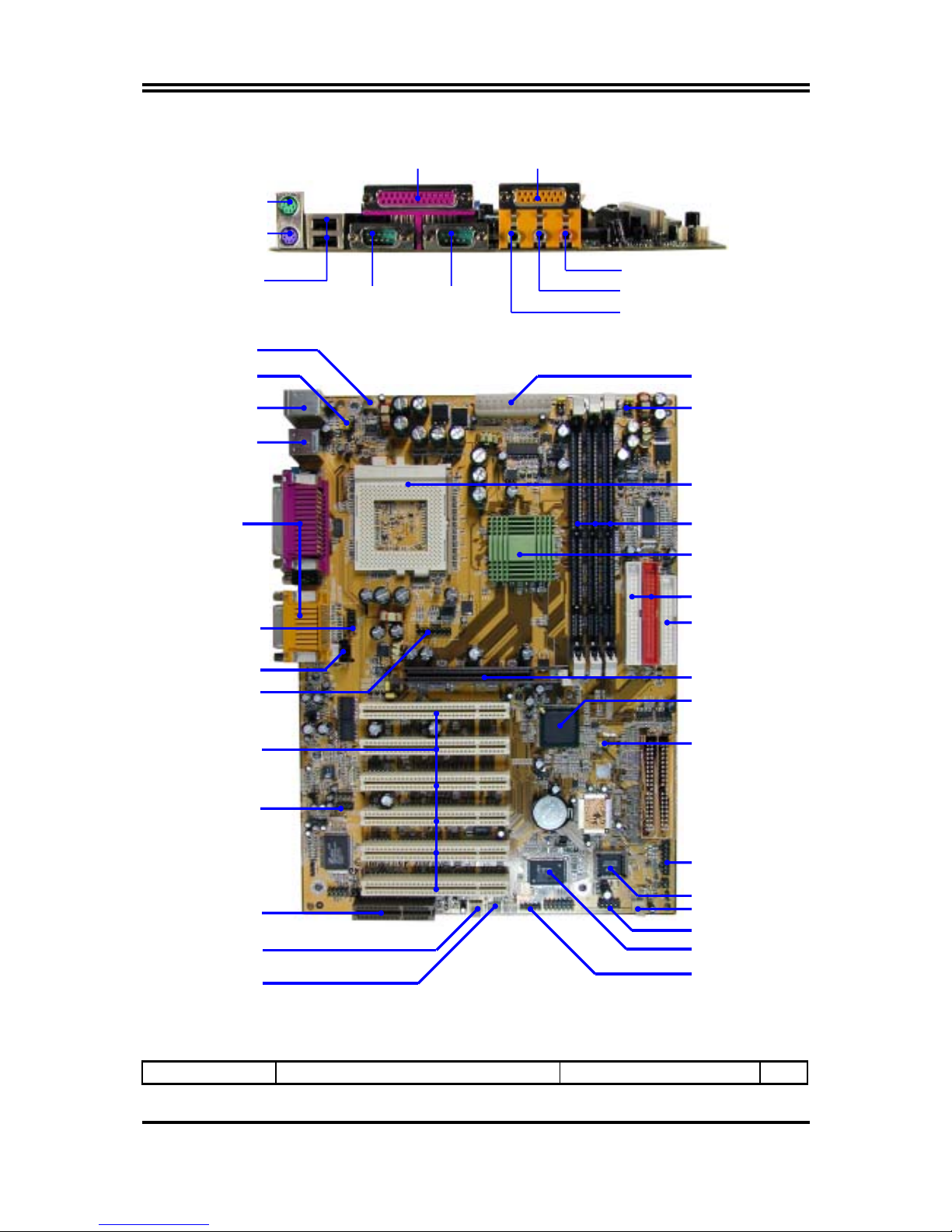
1-4 Layout Diagram & Jumper Setting
6
Jumpers
Jumper Name Description Page
COM1 COM2
PS/2 MOUSE
PS/2 Keyboard
USB
LINE-OUT
LINE-IN
MIC
PRINT GAME/MIDI PORT
PC99 Back Panel
Wake On LAN
FAN1
K/B Power ON
Jumper (JK1)
CNR Slot
Front Panel Audio
CD Audio
PCI Slot
FAN2
6 Channel Conn.
VGA Connector
370 CPU Socket
ITE 8712 Chip
Floppy Connector
Intel 815 Chip
Front Panel Connector
(JBAT)
Clear CMOS Jumper
ATX Power
Connector
USB Port (USB_B)
FAN3
2M bit ROM BIOS
CPU F.S.B. Clock
Select Jumper
(SW1,
SW2, SW3, SW4)
ATA 100 IDE
Connector
Intel 82801BA Chip
AGP Slot
IR Connector
DIMM Socket X3
PS2 KB/Mouse Port
USB Port
7
JS3, JS4
JS1, JS2
CPU & SDRAM Frequency Setting 3-pin Block
2-pin Block
p.8
JK1 Keyboard Power ON Function Setting 3-pin Block p.9
JBAT CMOS RAM Clear 3-pin Block p.9
Connectors
Connector Name Description Page
ATXPWR ATX Power Connector 20-pin Block p.17
CN1
(PS2 KB/MS)
PS/2 Mouse & PS/2 Keyboard
Connector
6-pin Female p.17
USB_A USB Port Connector 4-pin Connector p.17
PRINT Parallel Port Connector 25-pin Female p.17
GAME Audio/Game Connector 3 phone jack+15-pin Connector p.17
COM1/COM2 Serial Port COM1 Connector 9-pin Connector p.17
FDC Floppy Driver Connector 34-pin Block p.18
IDE1/IDE2 Primary/Secondary IDE Connector 40-pin Block p.18
Headers
Header Name Description Page
VGA VGA Port Headers 15-pin Block p.19
USB_B USB Port Headers 10-pin Block p.19
IDE LED IDE activity LED 2-pin Block p.19
TBLED Turbo LED switch 2-pin Block p.20
RESET Reset switch lead 2-pin Block p.20
SPKR Speaker connector 4-pin Block p.20
POWER LED Power LED 2-pin Block p.20
PWR BTN Power Button 2-pin Block p.20
WOL Wake On-LAN Headers 3-pin Block p.20
FAN1, FAN2, FAN3 FAN Speed Headers 3-pin Block p.21
IR IR infrared module Headers 5-pin Block p.21
AUDIO Line-In/Out, MIC header 9-pin Block p.22
CDIN1 CD Audio-In Headers 4-pin Block p.22
Expansion Sockets
Socket/Slot Name Description Page
ZIF Socket 370 CPU Socket 370-pin FC-PGA CPU Socket p.12
DIMM1, DIMM2
DIMM3
DIMM Module Socket 168-pin DIMM SDRAM Module
Expansion Socket
p.14
PCI1, PCI2, PCI3,
PCI4, PCI5, PCI6
PCI Slot 32-bit PCI Local Bus Expansion slots p.15
AGP AIMM /AGP 4X Mode Slot AIMM & AGP Expansion Slot p.16
CNR CNR Slot Communication Network Riser Slot
For 618TAF Only
Chapter 2
Hardware installation
8
2-1 Hardware installation Steps
Before using your computer, you had better complete the following steps:
1. Check motherboard setting
2. Install CPU
3. Install Memory
4. Install Expansion cards
5. Connect Ribbon cables, Panel wires, and power supply
6. Setup BIOS
7. Install software driver & utility
2-2 Checking Motherboard’s Jumper Setting
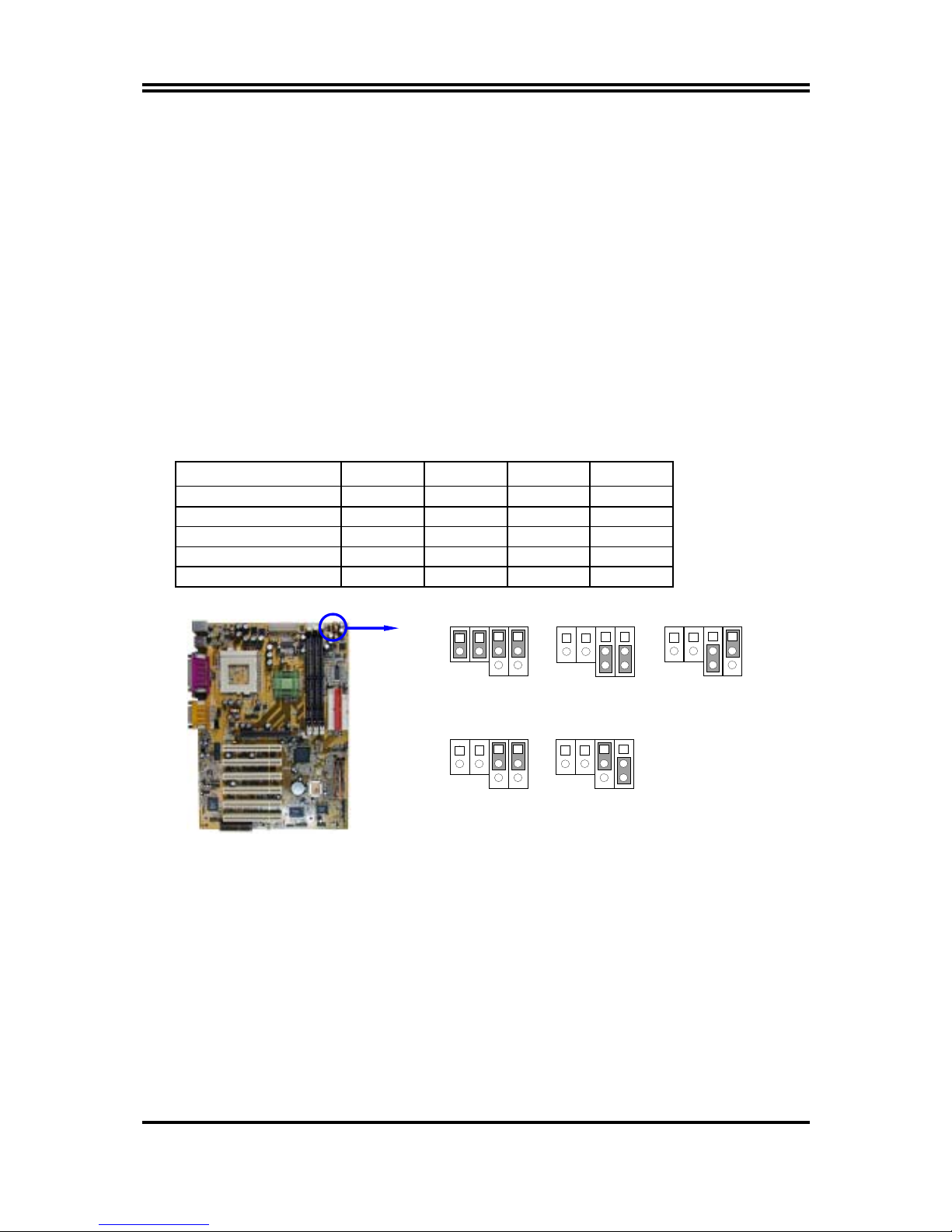
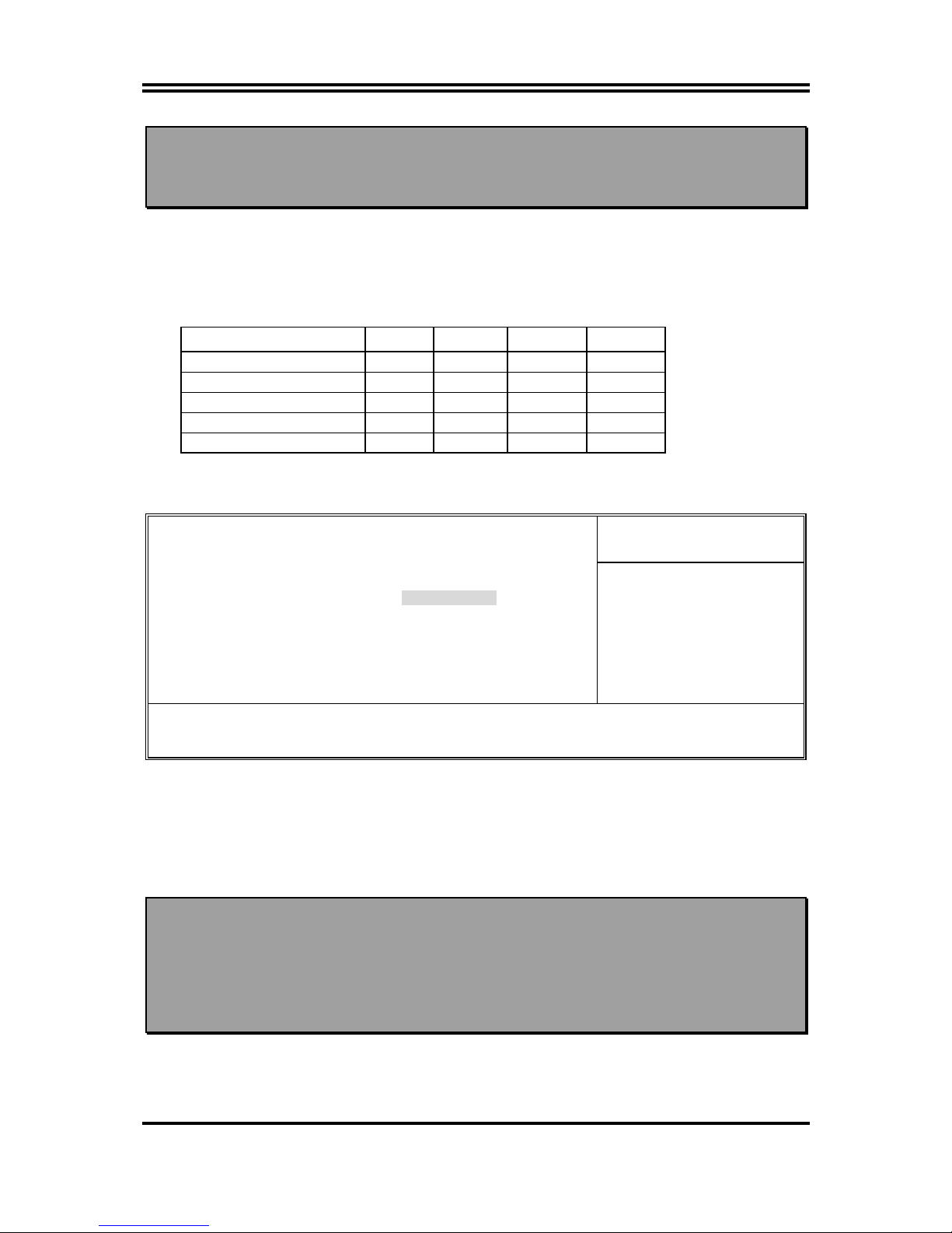
(1) CPU Host/SDRAM Clock setting: JS1, JS2, JS3, JS4
The motherboard’s CPU & SDRAM memory clock adjusted through jumper JS1,
JS2, JS3 & JS4. Table as below:
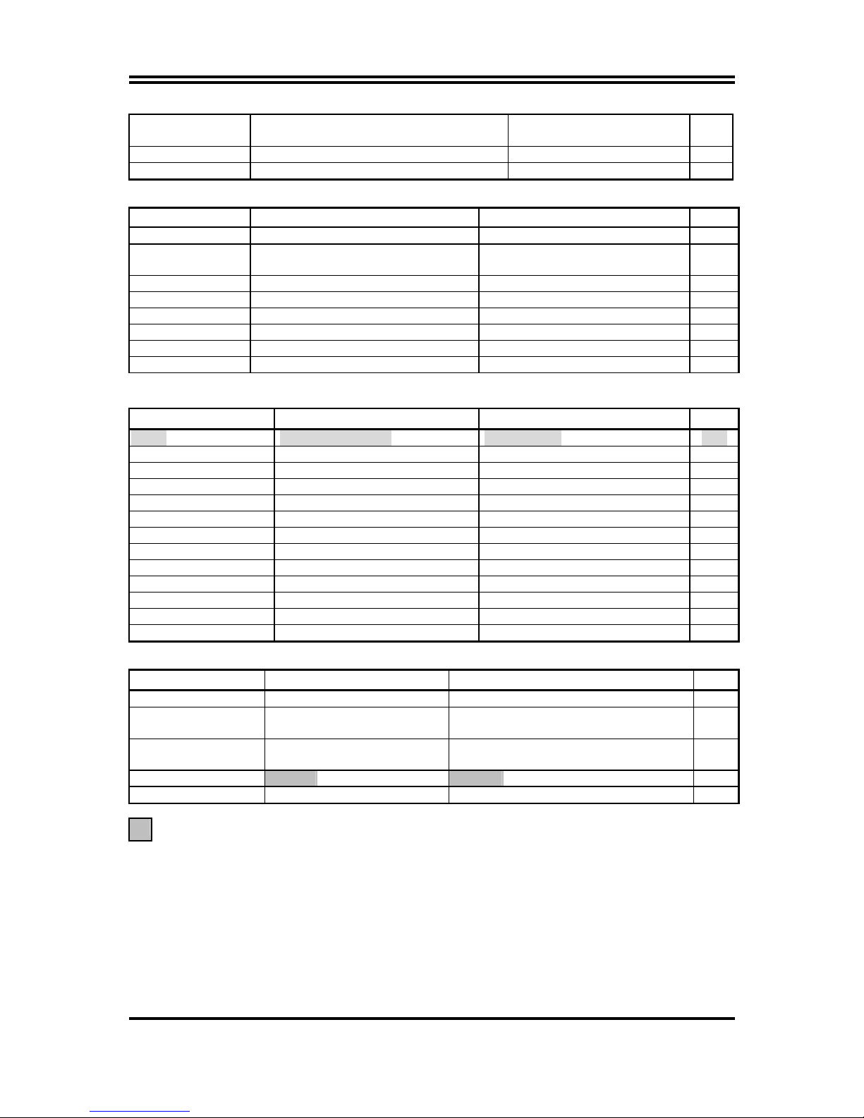
CPU/SDRAM (MHz) JS1 JS2 JS3 JS4
* AUTO ON ON 1-2 1-2
66/100
(Default)
OFF OFF 2-3 2-3
100/100 OFF OFF 2-3 1-2
133/100 OFF OFF 1-2 1-2
133/133 OFF OFF 1-2 2-3
CPU Host/SDRAM Clock Setting
1
3
AUTO
1
2
JS2
JS3
JS4
JS1
1
3
100/100
1
3
66/100
(
Default
)
1
2
JS2
JS3
JS4
JS1
1
2
JS2
JS3
JS4
JS1
1
3
133/100
1
2
JS2
JS3
JS4
JS1
1
3
133/133
1
2
JS2
JS3
JS4
JS1
∗ When jumper setting Auto it only can support CPU/SDRAM frequency at 66/100,
100/100, 133/100 MHz, we recommend setting 133/133 manually when use F.S.B.
133MHz CPU to increase performance.
In “Miscellaneous Control” section of CMOS Setup Utility, you can increase the
CPU clock step by step increase for over clocking possibility. Please refer to page
13 for more details.
(2) Keyboard Power On Function setting (3-pin) : JK1
This allows you to disable the keyboard power on function. Set the jumper to
enabled or disabled if you wish to use your keyboard (by pressing < >) to power on
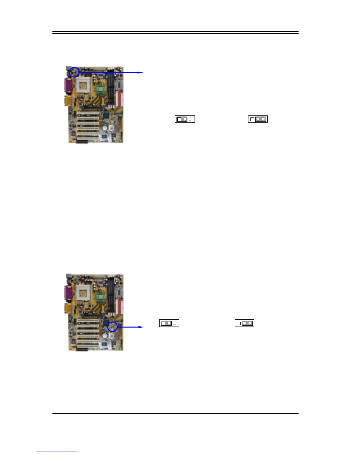
9
your computer, this feature requires an ATX power supply that can supply at least
300mA on the +5VSB lead. The default is set on disable.
Keyboard Power On Function
2-3 closed : Enabled
JK1
1 3
JK1
13
1-2 closed : Disabled (default)
(3) CMOS RAM Clear (3-pin) : JBAT
A battery must be used to retain the motherboard configuration in CMOS RAM
short 1-2 pins of JBAT to store the CMOS data.
To clear the CMOS, follow the procedure below:
1. Turn off the system and unplug the AC power
2. Remove ATX power cable from ATX power connector
3. Locate JBAT and short pins 2-3 for a few seconds
4. Return JBAT to its normal setting by shorting pins 1-2
5. Connect ATX power cable back to ATX power connector
Note: When should clear CMOS
1. Troubleshooting
2. Forget password
3. After over clocking system boot fail
CMOS RAM Clear Setting
2-3 closed : Clear CMOS
JBAT
13
JBAT
13
1-2 closed : Normal (default)
2-3 Install CPU

10
2-3-1 Glossary
Chipset (core logic) - two or more integrated circuits which control the interfaces
between the system processor, RAM, I/O devises, and adapter cards.
Processor socket - the socket used to mount the system processor on the motherboard.
Slot (AGP, PCI, ISA, RAM) - the slots used to mount adapter cards and system RAM.
AGP - Accelerated Graphics Port - a high speed interface for video cards; runs at 1X
(66MHz), 2X (133MHz), or 4X (266MHz).
PCI - Peripheral Component Interconnect - a high speed interface for video cards,
sound cards, network interface cards, and modems; runs at 33MHz.
Serial Port - a low speed interface typically used for mouse and external modems.
Parallel Port - a low speed interface typically used for printers.
PS/2 - a low speed interface used for mouse and keyboards.
USB - Universal Serial Bus - a medium speed interface typically used for mouse,
keyboards, scanners, and some digital cameras.
Sound (interface) - the interface between the sound card or integrated sound
connectors and speakers, MIC, game controllers, and MIDI sound devices.
BIOS (Basic Input/Output System) - the program logic used to boot up a computer and
establish the relationship between the various components.
Driver - software, which defines the characteristics of a device for use by another
device or other software.
Processor - the "Central Processing Unit" (CPU); the principal integrated circuit used
for doing the "computing" in "personal computer"
Front Side Bus Frequency
- The working frequency of the motherboard, which is
generated by the clock generator for CPU, DRAM and PCI BUS.
CPU L2 Cache
- The flash memory inside the CPU, normally Pentium III CPU has
256K or above, while Celeron CPU will have 128K.
The way to recognize the specification of CPU from the packing Pentium III 370
pins FC-PGA
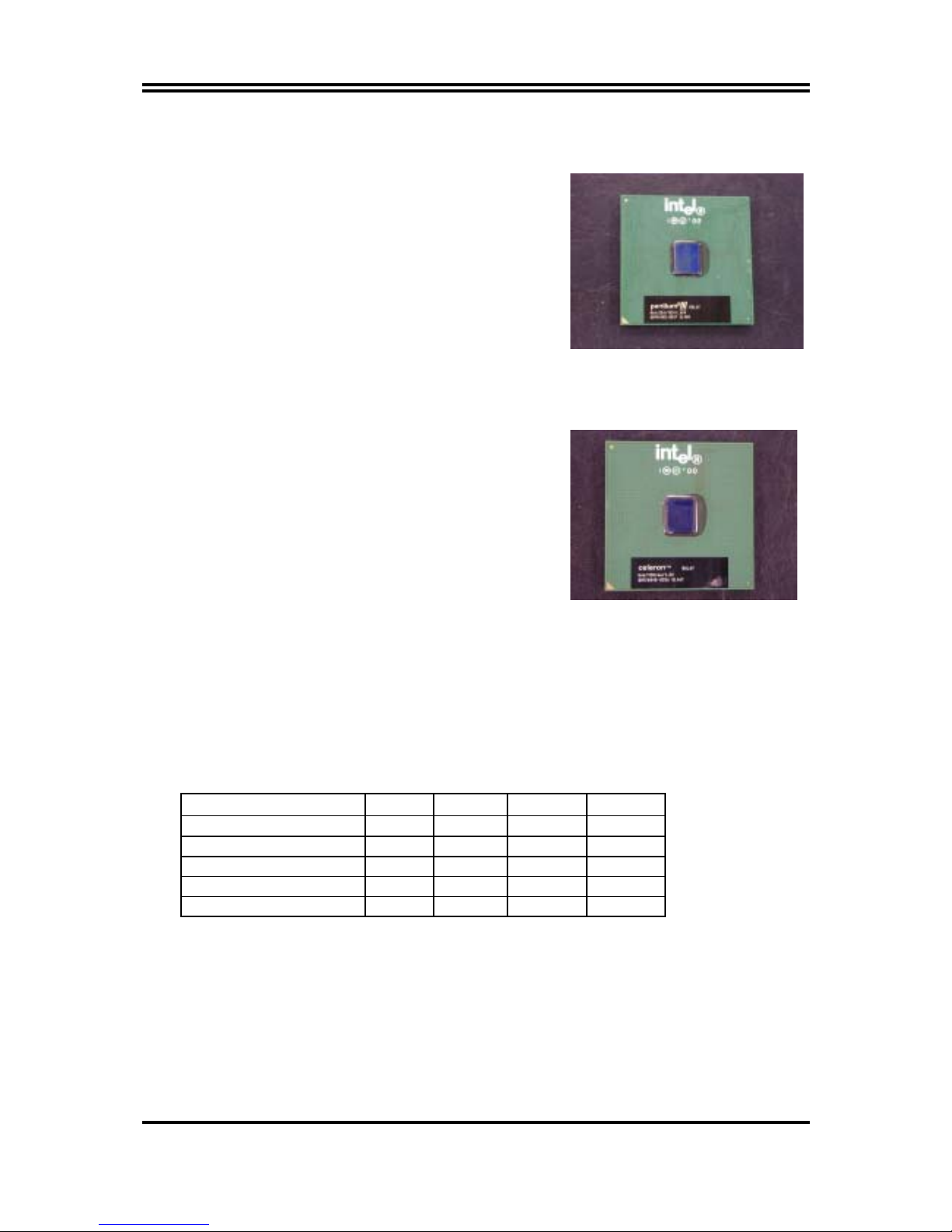
11
On the surface of the CPU as shown on the right picture, under the word of
“PENTIUM III” the code is:
RB 80526 P2 866 256
RB :
FC–PGA packing
P2 :
P2–133MHz front side bus frequency
PY–100MHz front side bus frequency
866 :
CPU internal frequency, where here is
866MHz
256 :
the size of L2 cache, where here is 256K
Celeron FC–PGA
On the surface of the CPU as shown on the right picture, under the word of “Celeron” the
code is:
566/128/66/1.5V
566 :
CPU internal frequency, where here is 566MHz
128 :
the size of L2 cache, where here is 128K
66 :
front side bus frequency, where here is 66MHz
1.5V :
the voltage for the CPU
2-3-2 Setting CPU Bus Clock & Memory Clock Jumper
Setting the front side bus frequency and SDRAM frequency
The motherboard uses jumper JS1, JS2, JS3 and JS4 for the front side bus frequency
and SDRAM frequency setting as shown from the table below:
CPU/SDRAM (MHz) JS1 JS2 JS3 JS4
AUTO ON ON 1-2 1-2
66/100
(Default)
OFF OFF 2-3 2-3
100/100 OFF OFF 2-3 1-2
133/100 OFF OFF 1-2 1-2
133/133 OFF OFF 1-2 2-3
Example: Using a Pentium III 866 CPU with front side bus frequency of 133MHz and
PC-133 SDRAM module, the setting of JS3 will be 1-2 and JS4 will be 2-3.
This sets both CPU BUS CLOCK and SDRAM CLOCK to be 133MHz.
For experience user looking for over clocking possibility, please refer to sec 2-3-4.
2-3-3 Install CPU
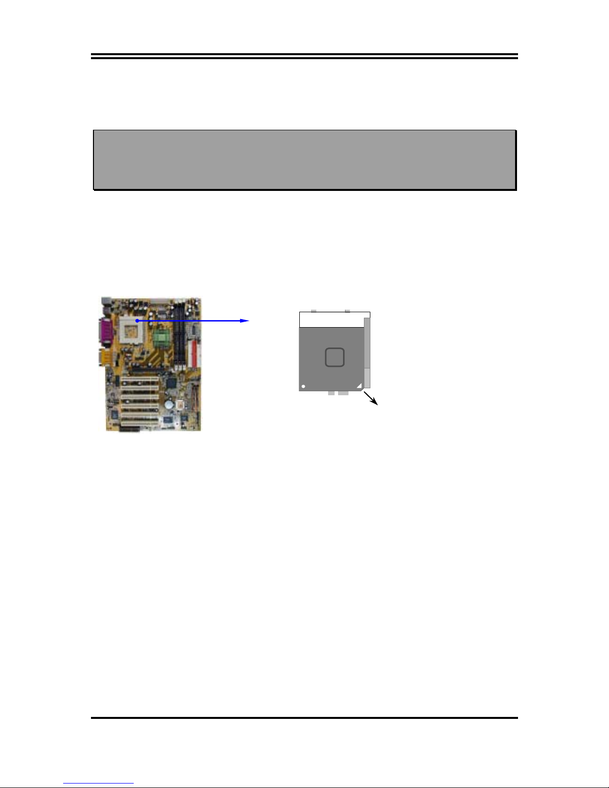
12
This motherboard provides a ZIF socket 370. The CPU that comes with the
motherboard should have a cooling FAN attached to prevent overheating. If this is not
the case, then purchase a correct cooling FAN before you turn on your system.
WARNING!
Be sure that there is sufficient air circulation across the processor’s
heatsink and CPU cooling FAN is working correctly, otherwise it may
cause the processor and motherboard overheat and damage, you may install
an auxiliary cooling FAN, if necessary.
To install a CPU, first turn off your system and remove its cover. Locate the ZIF
socket and open it by first pulling the level sideways away from the socket then
upward to a 90-degree angle. Insert the CPU with the correct orientation as shown
below. The notched corner should point toward the end of the level. Because the CPU
has a corner pin for two of the four corners, the CPU will only fit in the orientation as
shown.
CPU ZIF Socket 370
Colden Arrow
Pentium
III
Socket 370
Intel
When you put the CPU into the ZIF socket. No forces require to insert of the CPU,
then press the level to locate position slightly without any extra force.
2-3-4 Over clock Running
13
WARNING!
This section is for experienced motherboard installer only. Over
clocking can result in system instability or even shortening life of the
processor.
After setting the Jumper JS1, JS2, JS3, JS4 you can choose over clock running by
BIOS CMOS SETUP UTILITY. When you entered CMOS SETUP UTILITY, choose
“Miscellaneous Control” you will see the screen as below then.
You can choose the situation you want to try.
CPU/SDRAM (MHz) JS1 JS2 JS3 JS4
AUTO ON ON 1-2 1-2
66/100
(Default)
OFF OFF 2-3 2-3
100/100 OFF OFF 2-3 1-2
133/100 OFF OFF 1-2 1-2
133/133 OFF OFF 1-2 2-3
CMOS Setup Utility – Copyright(C) 1984-2001 Award Software
Miscellaneous Control
Item Help
CyrixIII Clock Ratio Default
Auto Detect DIMM/PCI Clk Enabled
Spread Spectrum Disabled
** Current Host Clock is 66Mhz **
CPU Host/SDRAM/PCI Clock 66/100/33Mhz
CPU Clock Ratio X 3
Menu Level >
CyrixIII CPU Ratio
Adjust
↑↓→←
Move Enter:Select +/-/PU/PD:Value F10:Save ESC:Exit F1:General Help
F5:Previous Values F6:Optimized Defaults F7:Standard Defaults
By press PageDown/PageUp key you can change the CPU Host/SDRAM/PCI Clock
When jumper setting CPU Host Clock 66MHz you can choose 66/100/33∼99/149/49MHz
When jumper setting CPU Host Clock 100MHz you can choose 100/100/33∼132/132/44MHz
When jumper setting CPU Host Clock 133MHz you can choose 133/100/33∼200/151/50MHz
When jumper setting CPU Host Clock 133MHz you can choose 133/133/33∼200/200/50MHz
WARNING!
The Design of this motherboard follows chipset and CPU vender’s design
guideline. Any attempts to push beyond product specification are not
recommended and you are taking your own risk to damage your system or
important data. Before over clocking, you must make sure your
components are able to tolerate such abnormal setting, especially CPU,
memory, hard disks, and VGA cards.
2-4 Install Memory
14
This motherboard provides three 168-pin DUAL INLINE MEMORY MODULES
(DIMM) sites for memory expansion available from minimum memory size of 32MB
to maximum memory size of 512MB SDRAM.
Valid Memory Configurations
DIMM
SDRAM Clock
DIMM1 DIMM2 DIMM3
DS DS DS
100MHz
SS SS SS
DS DS SS
133MHz
SS SS SS
According the specification when SDRAM clock is 133MHz only can support 2 pcs
Double Sided DIMMs
DS : Double Sided DIMM
SS : Single Sided DIMM
NOTE!
Make sure the total installed memory does not exceeds 512MB, otherwise
the system may hang during startup.
Generally, installing SDRAM modules to your motherboard is very easy, you can refer
to figure 2-4 to see what a 168-Pin PC100 & PC133 SDRAM module looks like.
DIMM2 (BANK2+BANK3)
DIMM1
(
BANK0+ BANK1
)
DIMM3 (BANK4+BANK5)
NOTE!
When you install DIMM module fully into the DIMM socket the eject
tab should be locked into the DIMM module very firmly and fit into its
indention on both sides.
WARNING!
For the SDRAM CLOCK is set at 133MHz, use only PC133-compliant
DIMMs. When this motherboard operate at 133Mhz, most system will
not even boot if non-compliant modules are used because of the strict
timing issues, if your DIMM are not PC133-compliant, set the SDRAM
clock to 100MHz to ensure system stability.
2-5 Expansion Cards
Figure 2-4
 Loading...