


"SecureJet Intelligent Appliance 8.1 - COMPANY CONFIDENTIAL"
Ref. SIA8.1_SRM Rev. B 1.0.0
SecureJet Intelligent Appliance 8.1
System Reference Manual
Revision B 1.0.0
April 2sd, 2014
Author: Patrick Touzeau
Contributing Editor: Xavier Raudin
Contact: jf.destalenx@jetmobile.com
1/51
(c)2014 Jetmobile Pte Ltd

"SecureJet Intelligent Appliance 8.1 - COMPANY CONFIDENTIAL"
Ref. SIA8.1_SRM Rev. B 1.0.0
TABLE OF CONTENTS
1 Introduction.............................................................................................................................................................. 4
2 Change History........................................................................................................................................................ 5
2.1 Document Change History ........................................................................................5
2.2 Board Changes.........................................................................................................5
2.2.1 Rev A 1.0.2.................................................................................................................................... 5
2.2.2 Rev B 1.0.0.................................................................................................................................... 5
3 SecureJet Intelligent Appliance 8.1 Overview.......................................................................................................... 6
3.1 SecureJet Intelligent Appliance 8.1 Features and Specification........................................6
3.2 Board Component Locations ......................................................................................7
4 SecureJet Intelligent Appliance 8.1 BOARD High Level Specification....................................................................9
4.1 Processor ................................................................................................................9
4.2 Memory ..................................................................................................................9
4.2.1 256MB DDR3L .............................................................................................................................. 9
4.2.2 2GB Embedded MMC ................................................................................................................... 9
4.2.3 MicroSD Connector ...................................................................................................................... 9
4.2.4 Boot Modes ................................................................................................................................... 9
4.3 Power Management ................................................................................................10
4.4 Serial Debug Port ...................................................................................................10
4.5 USB1 Host Port ......................................................................................................10
4.6 Power Sources .......................................................................................................10
4.7 Reset Button .........................................................................................................10
4.8 Power Button .........................................................................................................10
5 Detailed Hardware Design..................................................................................................................................... 12
5.1 Power Section ........................................................................................................12
5.1.1 TPS65217C PMIC ...................................................................................................................... 12
5.1.2 DC POWER................................................................................................................................. 13
5.1.3 Power Button .............................................................................................................................. 13
5.1.4 Power Consumption ................................................................................................................... 13
5.1.5 Processor Interfaces ................................................................................................................... 14
5.1.5.1 I2C0 ............................................................................................................................... 14
5.1.5.2 PMC_POWR_EN ........................................................................................................... 14
5.1.5.3 LDO_GOOD .................................................................................................................. 14
5.1.5.4 PMIC_PGOOD .............................................................................................................. 14
5.1.5.5 WAKEUP ....................................................................................................................... 14
5.1.5.6 PMIC_INT ...................................................................................................................... 14
5.1.6 Power Rails ................................................................................................................................. 15
5.1.6.1 VRTC Rail ...................................................................................................................... 15
5.1.6.2 VDD_3V3A Rail ............................................................................................................. 15
5.1.6.3 VDD_3V3B Rail ............................................................................................................. 15
5.1.6.4 VDD_1V8 Rail ................................................................................................................ 16
5.1.6.5 VDD_CORE Rail ............................................................................................................ 16
5.1.6.6 VDD_MPU Rail .............................................................................................................. 16
5.1.6.7 VDDS_DDR Rail ............................................................................................................ 16
5.1.6.8 Power Sequencing.......................................................................................................... 16
5.1.7 TPS65217C Power Up Process ................................................................................................. 17
5.1.8 Processor Control Interface ........................................................................................................ 18
5.1.9 Low Power Mode Support ........................................................................................................... 18
5.1.9.1 RTC Only ....................................................................................................................... 18
5.1.9.2 RTC Plus DDR ............................................................................................................... 18
5.1.9.3 Voltage Scaling .............................................................................................................. 18
5.2 Sitara XAM3352BZCZ Processor ...............................................................................19
5.2.1 Description .................................................................................................................................. 19
5.3 DDR3L Memory ......................................................................................................20
5.3.1 Memory Device ........................................................................................................................... 20
5.3.2 DDR3L Memory Design .............................................................................................................. 20
5.3.3 Power Rails ................................................................................................................................. 21
2/51
(c)2014 Jetmobile Pte Ltd

"SecureJet Intelligent Appliance 8.1 - COMPANY CONFIDENTIAL"
Ref. SIA8.1_SRM Rev. B 1.0.0
5.3.4 VREF .......................................................................................................................................... 21
5.4 2GB eMMC Memory ................................................................................................23
5.4.1 6.4.1 eMMC Device .................................................................................................................... 23
5.4.2 eMMC Circuit Design .................................................................................................................. 24
5.5 Micro Secure Digital ...............................................................................................26
5.5.1 microSD Design .......................................................................................................................... 26
5.6 User LEDs .............................................................................................................27
5.7 Boot Configuration .................................................................................................28
5.7.1 Default Boot Options ................................................................................................................... 28
5.8 10/100 Ethernet ....................................................................................................29
5.8.1 Ethernet Processor Interface ...................................................................................................... 29
5.8.2 Ethernet Connector Interface ...................................................................................................... 31
5.8.3 Ethernet PHY Power, Reset, and Clocks .................................................................................... 31
5.8.3.1 VDD_3V3B Rail ............................................................................................................. 31
5.8.3.2 VDD_PHYA Rail ............................................................................................................. 31
5.8.3.3 PHY_VDDCR Rail ......................................................................................................... 31
5.8.3.4 SYS_RESET .................................................................................................................. 32
5.8.3.5 Clock Signals ................................................................................................................. 32
5.8.4 LAN8710A Mode Pins ................................................................................................................. 32
5.9 USB Host...............................................................................................................33
5.9.1 Power Switch .............................................................................................................................. 33
5.9.2 ESD Protection ........................................................................................................................... 33
5.9.3 Filter Options .............................................................................................................................. 33
6 Connectors............................................................................................................................................................. 34
7 SCHEMATIC.......................................................................................................................................................... 35
3/51
(c)2014 Jetmobile Pte Ltd

"SecureJet Intelligent Appliance 8.1 - COMPANY CONFIDENTIAL"
Ref. SIA8.1_SRM Rev. B 1.0.0
1 INTRODUCTION
This document is the System Reference Manual for the SecureJet Intelligent Appliance 8.1
board and covers its use and design. The board will primarily be referred to in the remainder of
this document simply as the board, although it may also be referred to as the SecureJet
Intelligent Appliance 8.1 board as a reminder.
4/51
(c)2014 Jetmobile Pte Ltd

"SecureJet Intelligent Appliance 8.1 - COMPANY CONFIDENTIAL"
Ref. SIA8.1_SRM Rev. B 1.0.0
2 CHANGE HISTORY
This section describes the change history of this document and board. Document changes are
not always a result of a board change. A board change will always result in a document
change.
2.1 Document Change History
Rev Changes Date By
A 0.0.1 Preliminary August 19th, 2013 PTU
A 1.0.2 Add Jetmobile logo contact product name, update footer
and header.
February 28th, 2014 PTU
B 1.0.0 Main changes : reset key affected to GPIO, update RTC
power, mDDR power planes (board)
March 12th, 2014 PTU
2.2 Board Changes
2.2.1 Rev A 1.0.2
This is the initial production release of the board. We will be tracking changes from this point
forward.
2.2.2 Rev B 1.0.0
Lidt of modifications :
• Change required PCB revision to B.
• Change PCB Copyrigth 2014 labels.
• Reset key is connected to GPIO2_1.
• RTC power is managed by an external LDO 1.8V U203.
• Change Ethernet Phy address : R934 connected, R923 not connected.
• Change C556 value to 1uF.
• Change R443 value to 100 ohms.
• FB400 connected (Ferrite Bead 150 Ohm 800mA connected).
• Noise issues was observed where the clock oscillator was getting hit due to a suspected
issue in ground bounce. R2 and R3 zero ohm resistors were added to connect the
OSC_GND to the system ground.
• Changes C300 to 2.2uF. This resolved an issue we were seeing in a few boards where
the board would not boot in 1 in 20 tries.
5/51
(c)2014 Jetmobile Pte Ltd

"SecureJet Intelligent Appliance 8.1 - COMPANY CONFIDENTIAL"
Ref. SIA8.1_SRM Rev. B 1.0.0
3 SECUREJET INTELLIGENT APPLIANCE 8.1 OVERVIEW
The board is designed by KWETCH embedded Systems.
3.1 SecureJet Intelligent Appliance 8.1 Features and Specification
This section covers the specifications and features of the board and provides a high level
description of the major components and interfaces that make up the board.
Tableau 1 : provides a list of the features.
Features
Processor
SDRAM Me mory 256 MB DDR3L 40 0 Mhz
Onboard Flash 2GB 8bit Embedded MMC
PMIC TPS652 17C PMIC regulator and one additional LDO
Power Source miniUSB USB or DC Jack
Indicator 2 User co ntrollable LED's integrated into button, 4 Ethernet
HS USB 2.0 Hos t Port Access to USB1 , type A soc ket, 50 0mA LS/F S/HS
Serial Port UART0 access via 6 pin 3.3V TTL Header, Header is populated
Ethernet 1 10/1 00, RJ4 5 w ith LED's
Ethernet 2 10/1 00, RJ4 5 w ith LED's
SD/MMC Connector MicroSD, 3.3V
User Input
Audio Buzz er
RTC RTC function with LiOn battery
Expension Connectors Pow er 5V, 3.3V, USB0 client mode, GPIO...
Weigth TBD
PCB TBD
Power 5/9/ 12 DC
Sitara AM335 2BZCZ8 00
800M hz
Reset Butto n
Boo t Button
Pow er Button
6/51
(c)2014 Jetmobile Pte Ltd
Tableau 1: SecureJet Intelligent Appliance 8.1 feature list
"SecureJet Intelligent Appliance 8.1 - COMPANY CONFIDENTIAL"
Ref. SIA8.1_SRM Rev. B 1.0.0
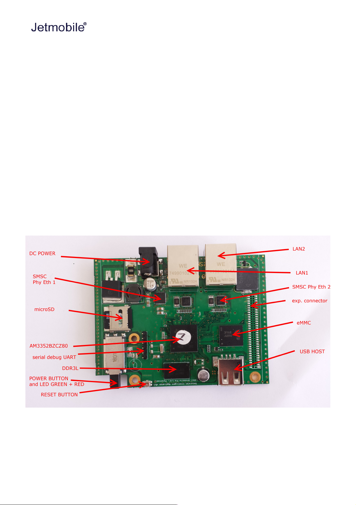
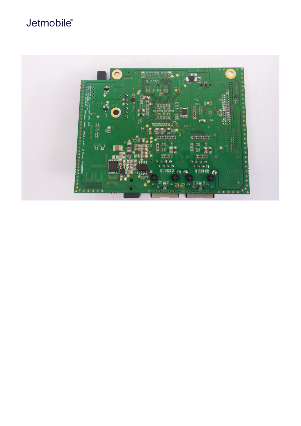
3.2 Board Component Locations
This section describes the key components on the board. It provides information on their
location and function. Familiarize yourself with the various components on the board.
DC Power is the main DC input that accepts 5V or 9V or 12V DCpower.
Power Button alerts the processor to initiate the power down sequence, 2 LED are
integrated into power button.
10/100 Ethernet are the connection to the LAN1 and LAN2.
Serial Debug is the serial debug port.
USB Host can be connected different USB interfaces such as Wi-Fi, BT, Keyboard, etc.
Extension connector will be used to connect SSD later
BOOT switch can be used to force a boot from the microSD card if the power is cycled on
the board, removing power and reapplying the power to the board.
Reset Button allows the user to reset product with factory setting.
microSD slot is where a microSD card can be installed.
Sitara AM3352BZCZ80 is the processor for the board.
Micron 256MB DDR3L is the Dual Data Rate RAM memory.
TPS65217C PMIC provides the power rails to the various components on the board.
SMSC Ethernet PHY is the physical interface to the network.
Micron eMMC is an onboard MMC chip that holds up to 2GB of data
7/51
(c)2014 Jetmobile Pte Ltd
"SecureJet Intelligent Appliance 8.1 - COMPANY CONFIDENTIAL"
Ref. SIA8.1_SRM Rev. B 1.0.0
8/51
(c)2014 Jetmobile Pte Ltd

"SecureJet Intelligent Appliance 8.1 - COMPANY CONFIDENTIAL"
Ref. SIA8.1_SRM Rev. B 1.0.0
4 SECUREJET INTELLIGENT APPLIANCE 8.1 BOARD HIGH
LEVEL SPECIFICATION
This section provides the high level specification of the SecureJet Intelligent Appliance 8.1 board.
4.1 Processor
For the initial release, the board uses the Sitara XAM3359BZCZ processor in the 15x15
package.
4.2 Memory
Described in the following sections are the three memory devices found on the board.
4.2.1 256MB DDR3L
A single 128Mb x16 DDR3L 2Gb (256MB) memory device is used. The memory used is the
MT41K128M1 from Micron. It will operate at a clock frequency of 400MHz yielding an effective
rate of 800MHZ on the DDR3L bus allowing for 1.6GB/S of DDR3L memory bandwidth.
4.2.2 2GB Embedded MMC
A single 2GB embedded MMC (eMMC) device is on the board. The device connects to the MMC1
port of the processor, allowing for 8bit wide access. Default boot mode for the board will be
MMC1 with an option to change it to MMC0, the SD card slot, for booting from the SD card as a
result of removing and reapplying the power to the board. Simply pressing the reset button will
not change the boot mode. MMC0 cannot be used in 8Bit mode because the lower data pins are
located on the pins used by the Ethernet port. This does not interfere with SD card operation
but it does make it unsuitable for use as an eMMC port if the 8 bit feature is needed.
4.2.3 MicroSD Connector
The board is equipped with a single microSD connector to act as the secondary boot source for
the board and, if selected as such, can be the primary boot source. The connector will support
larger capacity microSD cards. The microSD card is not provided with the board. Booting from
MMC0 will be used to flash the eMMC in the production environment or can be used by the user
to update the SW as needed.
4.2.4 Boot Modes
As mentioned earlier, there are four boot modes:
eMMC Boot…This is the default boot mode and will allow for the fastest boot time
and will enable the board to boot out of the box using.
SD Boot…This mode will boot from the microSD slot. This mode can be used to
override what is on the eMMC device and can be used to program the eMMC when
used in the manufacturing process or for field updates.
Serial Boot…This mode will use the serial port to allow downloading of the
software direct. A separate USB to serial cable is required to use this port.
USB Boot…This mode supports booting over the USB port.
Software to support USB and serial boot modes is not provided. Please contact
KWETCH Embedded Systems for support of this feature.
A switch is provided to allow switching between the modes.
9/51
(c)2014 Jetmobile Pte Ltd

"SecureJet Intelligent Appliance 8.1 - COMPANY CONFIDENTIAL"
Ref. SIA8.1_SRM Rev. B 1.0.0
Holding the boot switch down during a removal and reapplication of power without a
microSD card inserted will force the boot source to be the USB port and if nothing is
detected on the USB client port, it will go to the serial port for download.
Without holding the switch, the board will boot try to boot from the eMMC. If it is
empty, then it will try booting from the microSD slot, followed by the serial port, and
then the USB port.
If you hold the boot switch down during the removal and reapplication of power to the
board, and you have a microSD card inserted with a bootable image, the board will boot
from the microSD card.
NOTE: Pressing the RESET button on the board will NOT result in a change of the
boot mode. You MUST remove power and reapply power to change the boot mode.
The boot pins are sampled during power on reset from the PMIC to the processor.
The reset button on the board is a warm reset only and will not force a boot mode
change.
4.3 Power Management
The TPS65217C power management device is used along with a separate LDO to provide
power to the system. The TPS65217C version provides for the proper voltages required for
the DDR3L and the processor. DDR3L requires 1.35V.
An external LDO TL5209 provides the 3.3V rail for the rest of the board.
4.4 Serial Debug Port
Serial debug is provided via UART0 on the processor via a single 1x6 pin header. In order to
use the interface a USB to TTL adapter will be required. The header is compatible with the one
provided by FTDI and can be purchased for about $12 to $20 from various sources. Signals
supported are TX and RX. None of the handshake signals are supported.
4.5 USB1 Host Port
On the board is a single USB Type A female connector with full LS/FS/HS Host support that
connects to USB1 on the processor. The port can provide power on/off control and up to 500mA
of current at 5V. Under USB power, the board will not be able to supply the full 500mA, but
should be sufficient to supply enough current for a lower power USB device supplying power
between 50 to 100mA.
4.6 Power Sources
The board can be powered from four different sources:
A 12VDC, 9VDC or 5VDC 1A power supply plugged into the DC connector.
A power supply with a USB connector.
The USB port is limited to 500mA by the Power Management IC. It is possible to change the
settings in the TPS65217C to increase this current, but only after the initial boot.
4.7 Reset Button
When pressed during systems boot will reset factory setting.
4.8 Power Button
A power button is provided. This button takes advantage of the input to the PMIC for power
down features. These features include:
10/51
(c)2014 Jetmobile Pte Ltd

"SecureJet Intelligent Appliance 8.1 - COMPANY CONFIDENTIAL"
Ref. SIA8.1_SRM Rev. B 1.0.0
Interrupt is sent to the processor to facilitate an orderly shutdown to save files and to un-
mount drives.
No sleep mode since the unit works as a LAN switch and the printer would be unreachable.
If you hold the button down the board will power off and the power LED turns off.
If you continue to hold it, the board will power back up completing a power cycle.
11/51
(c)2014 Jetmobile Pte Ltd

"SecureJet Intelligent Appliance 8.1 - COMPANY CONFIDENTIAL"
Ref. SIA8.1_SRM Rev. B 1.0.0
5 DETAILED HARDWARE DESIGN
This section provides a detailed description of the Hardware design. This can be useful for
interfacing, writing drivers, or using it to help modify specifics of your own design.
5.1 Power Section
Figure xxx is the high level block diagram of the power section of the board.
This section describes the power section of the design and all the functions performed by the
TPS65217C.
5.1.1 TPS65217C PMIC
The main Power Management IC (PMIC) in the system is the TPS65217C which is a single chip
power management IC consisting of a linear dual-input power path, three step-down
converters, and four LDOs. LDO stands for Low Drop Out. If you want to know more about an
LDO, you can go to http://en.wikipedia.org/wiki/Low-dropout_regulator. If you want to learn
more about step-down converters, you can go to http://en.wikipedia.org/wiki/DC-to-
DC_converter
The system is supplied by DC adapter. Three high-efficiency 2.25MHz step-down converters are
targeted at providing the core voltage, MPU, and memory voltage for the board.
The step-down converters enter a low power mode at light load for maximum efficiency across
the widest possible range of load currents. For low-noise applications the devices can be forced
into fixed frequency PWM using the I2C interface. The step-down converters allow the use of
small inductors and capacitors to achieve a small footprint solution size.
LDO1 and LDO2 are intended to support system standby mode. In normal operation, they can
support up to 100mA each. LDO3 and LDO4 can support up to 285mA each.
By default only LDO1 is always ON but any rail can be configured to remain up in SLEEP state.
In particular the DCDC converters can remain up in a low-power PFM mode to support
processor suspend mode. The TPS65217C offers flexible power-up and power-down
12/51
(c)2014 Jetmobile Pte Ltd

"SecureJet Intelligent Appliance 8.1 - COMPANY CONFIDENTIAL"
Ref. SIA8.1_SRM Rev. B 1.0.0
sequencing and several house-keeping functions such as power-good output, pushbutton
monitor, hardware reset function and temperature sensor to protect the battery.
For more information on the TPS65217C, refer to http://www.ti.com/product/tps65217C
5.1.2 DC POWER
An input DC power adapter 5V or 9V or 12V DC is plug into the board. A LDO LM25085 convert
the input DC power into 5V DC for the complete system.
5.1.3 Power Button
A power button is connected to the input of the TPS65217C. This is a momentary switch.
If you push the button the TPS65217C will send an interrupt to the processor. It is up to the
processor to then pull the PMIC_POWER_EN pin low at the correct time to power down the
board. At this point, the PMIC is still active, assuming that the power input was not removed.
Pressing the power button will cause the board to power up again if the processor puts the
board in the power off mode.
In power off mode, the RTC rail is still active, keeping the RTC powered. The RTC is powered
using a battery.
5.1.4 Power Consumption
The power consumption of the board varies based on power scenarios and the board boot
processes.
13/51
(c)2014 Jetmobile Pte Ltd
Illustra
tion 1: Input DC power

"SecureJet Intelligent Appliance 8.1 - COMPANY CONFIDENTIAL"
Ref. SIA8.1_SRM Rev. B 1.0.0
5.1.5 Processor Interfaces
The processor interacts with the TPS65217C via several different signals. Each of these
signals is described below.
5.1.5.1 I2C0
I2C0 is the control interface between the processor and the TPS65217C. It allows the
processor to control the registers inside the TPS65217C for such things as voltage scaling and
switching of the input rails.
5.1.5.2 PMC_POWR_EN
On power up the VDD_RTC rail activates first. After the RTC circuitry in the processor has
activated it instructs the TPS65217C to initiate a full power up cycle by activating the
PMIC_POWR_EN signal by taking it HI. When powering down, the processor can take this pin
low to start the power down process.
5.1.5.3 LDO_GOOD
This signal connects to the RTC_PORZn signal, RTC power on reset. The small n indicates that
the signal is an active low signal. Word processors seem to be unable to put a bar over a word
so the n is commonly used in electronics. As the RTC circuitry comes up first, this signal
indicates that the LDOs, the 1.8V VRTC rail, is up and stable. This starts the power up process.
5.1.5.4 PMIC_PGOOD
Once all the rails are up, the PMIC_PGOOD signal goes high. This releases the PORZn signal
on the processor which was holding the processor reset.
5.1.5.5 WAKEUP
The WAKEUP signal from the TPS65217C is connected to the EXT_WAKEUP signal on the
processor. This is used to wake up the processor when it is in a sleep mode. When an event is
detected by the TPS65217C, such as the power button being pressed, it generates this signal.
5.1.5.6 PMIC_INT
The PMIC_INT signal is an interrupt signal to the processor. Pressing the power button will
send an interrupt to the processor allowing it to implement a power down mode in an orderly
fashion, go into sleep mode, or cause it to wake up from a sleep mode. All of these require SW
support.
14/51
(c)2014 Jetmobile Pte Ltd

"SecureJet Intelligent Appliance 8.1 - COMPANY CONFIDENTIAL"
Ref. SIA8.1_SRM Rev. B 1.0.0
5.1.6 Power Rails
The following illustration shows the connections of each of the rails from the TPS65217C.
5.1.6.1 VRTC Rail
The VRTC rail is a 1.8V rail and it is supplied by the U203 LP2985-18.
5.1.6.2 VDD_3V3A Rail
The VDD_3V3A rail is supplied by the TPS65217C and provides the 3.3V for the processor
rails and can provide up to 400mA.
5.1.6.3 VDD_3V3B Rail
The current supplied by the VDD_3V3A rail is not sufficient to power all of the 3.3V rails on
the board. So a second LDO is supplied, U200, a TL5209A, which sources the VDD_3V3B rail.
It is powered up just after the VDD_3V3A rail.
15/51
(c)2014 Jetmobile Pte Ltd
Illustration 2: TPS65217C power rails

"SecureJet Intelligent Appliance 8.1 - COMPANY CONFIDENTIAL"
Ref. SIA8.1_SRM Rev. B 1.0.0
5.1.6.4 VDD_1V8 Rail
The VDD_1V8 rail can deliver up to 400mA and provides the power required for the 1.8V rails
on the processor and the HDMI framer. This rail is not accessible for use anywhere else on the
board.
5.1.6.5 VDD_CORE Rail
The VDD_CORE rail can deliver up to 1.2A at 1.1V. This rail is not accessible for use anywhere
else on the board and connects only to the processor. This rail is fixed at 1.1V and is should not
be adjusted by SW using the PMIC. If you do, then the processor will no longer process.
5.1.6.6 VDD_MPU Rail
The VDD_MPU rail can deliver up to 1.2A. This rail is not accessible for use anywhere else on
the board and connects only to the processor. This rail defaults to 1.1V and can be scaled up to
allow for higher frequency operation. Changing of the voltage is set via the I2C interface from
the processor.
5.1.6.7 VDDS_DDR Rail
The VDDS_DDR rail defaults to 1.5V to support the DDR3L rails and can deliver up to 1.2A. It
is possible to adjust this voltage rail down to 1.35V for lower power operation of the DDR3L
device. Only DDR3L devices can support this voltage setting of 1.35V.
5.1.6.8 Power Sequencing
The power up process is consists of several stages and events. Figure XXXX describes the
events that make up the power up process for the processor from the PMIC. This diagram
is used elsewhere to convey additional information. I saw no need to bust it up into
smaller diagrams. It is from the processor datasheet supplied by Texas Instruments.
16/51
(c)2014 Jetmobile Pte Ltd
Illustration 3: VDD_3V3B power rail

"SecureJet Intelligent Appliance 8.1 - COMPANY CONFIDENTIAL"
Ref. SIA8.1_SRM Rev. B 1.0.0
The voltage rail sequencing for the TPS65217C as it powers up and the voltages on each rail.
The power sequencing starts at 15 and then goes to one. That is the way the TPS65217C is
configured. You can refer to the TPS65217C datasheet for more information.
5.1.7 TPS65217C Power Up Process
The interface between the TPS65217C and the processor. It is a cut from the PDF form of the
schematic and reflects what is on the schematic.
17/51
(c)2014 Jetmobile Pte Ltd
Illustration 4: Power sequence
Illustration 5: TPS65217C interface with processor

"SecureJet Intelligent Appliance 8.1 - COMPANY CONFIDENTIAL"
Ref. SIA8.1_SRM Rev. B 1.0.0
When voltage is applied, DC or USB, the TPS65217C connects the power to the SYS output
pin which drives the switchers and LDOs in the TPS65217C.
At power up all switchers and LDOs are off except for the VRTC LDO (1.8V), which provides
power to the VRTC rail and controls the RTC_PORZn input pin to the processor, which starts
the power up process of the processor. Once the RTC rail powers up, the RTC_PORZn pin,
driven by the LDO_PGOOD signal from the TPS65217C, of the processor is released.
Once the RTC_PORZn reset is released, the processor starts the initialization process. After
the RTC stabilizes, the processor launches the rest of the power up process by activating the
PMIC_POWER_EN signal that is connected to the TPS65217C which starts the TPS65217C
power up process.
The LDO_PGOOD signal is provided by the TPS65217C to the processor. As this signal is
1.8V from the TPS65217C by virtue of the TPS65217C VIO rail being set to 1.8V, and the
RTC_PORZ signal on the processor is 3.3V, a voltage level shifter, U4, is used. Once the LDOs
and switchers are up on the TPS65217C, this signal goes active releasing the processor. The
LDOs on the TPS65217C are used to power the VRTC rail on the processor.
5.1.8 Processor Control Interface
Figure xxxx above shows two interfaces between the processor and the TPS65217C used for
control after the power up sequence has completed.
The first is the I2C0 bus. This allows the processor to turn on and off rails and to set the
voltage levels of each regulator to supports such things as voltage scaling.
The second is the interrupt signal. This allows the TPS65217C to alert the processor when
there is an event, such as when the optional power button is pressed. The interrupt is an open
drain output which makes it easy to interface to 3.3V of the processor.
5.1.9 Low Power Mode Support
This section covers three general power down modes that are available. These modes are only
described from a Hardware perspective as it relates to the HW design.
5.1.9.1 RTC Only
In this mode all rails are turned off except the VDD_RTC. The processor will need to turn off
all the rails to enter this mode. The VDD_RTC staying on will keep the RTC active and provide
for the wakeup interfaces to be active to respond to a wake up event.
5.1.9.2 RTC Plus DDR
In this mode all rails are turned off except the VDD_RTC and the VDDS_DDR, which powers
the DDR3L memory. The processor will need to turn off all the rails to enter this mode. The
VDD_RTC staying on will keep the RTC active and provide for the wakeup interfaces to be
active to respond to a wake up event.
The VDDS_DDR rail to the DDR3L is provided by the 1.5V rail of the TPS65217C and with
VDDS_DDR active, the DDR3L can be placed in a self refresh mode by the processor prior to
power down which allows the memory data to be saved.
Currently, this feature is not included in the software release.
5.1.9.3 Voltage Scaling
For a mode where the lowest power is possible without going to sleep, this mode allows the
voltage on the ARM processor to be lowered along with slowing the processor frequency down.
The I2C0 bus is used to control the voltage scaling function in the TPS65217C.
18/51
(c)2014 Jetmobile Pte Ltd

"SecureJet Intelligent Appliance 8.1 - COMPANY CONFIDENTIAL"
Ref. SIA8.1_SRM Rev. B 1.0.0
5.2 Sitara XAM3352BZCZ Processor
The board is designed to use either the Sitara AM3352BZCZ processor in the 15 x 15 package.
5.2.1 Description
A high level block diagram of the processor. For more information on the processor, go to
http://www.ti.com/product/am3352
19/51
(c)2014 Jetmobile Pte Ltd
Illustration 6: 5.2 Sitara XAM3352BZCZ Processor

"SecureJet Intelligent Appliance 8.1 - COMPANY CONFIDENTIAL"
Ref. SIA8.1_SRM Rev. B 1.0.0
5.3 DDR3L Memory
The SecureJet Intelligent Appliance 8.1 board uses a single MT41K128M16JT-125 256MB
DDR3L device from Micron that interfaces to the processor over 16 data lines, 16 address lines,
and 14 control lines. The following sections provide more details on the design.
5.3.1 Memory Device
The design supports the standard DDR3 and DDR3L x16 devices and us built using the DDR3L.
A single x16 device is used on the board and there is no support for two x8 devices. The DDR3
devices work at 1.5V and the DDR3L devices can work down to 1.35V to achieve lower power.
The specific Micron device used is the MT41K128M16JT-125. It comes in a 96-BALL FBGA
package with 0.8 mil pitch. Other standard DDR3 devices can also be supported, but the
DDR3L is the lower power device and was chosen for its ability to work at 1.5V or 1.35V. The
standard frequency that the DDR3L is run at on the board is 400MHZ.
5.3.2 DDR3L Memory Design
20/51
(c)2014 Jetmobile Pte Ltd
Illustration 7: DDR3L schematic

"SecureJet Intelligent Appliance 8.1 - COMPANY CONFIDENTIAL"
Ref. SIA8.1_SRM Rev. B 1.0.0
The schematic for the DDR3L memory device. Each of the groups of signals is described in the
following lines.
Address Lines: Provide the row address for ACTIVATE commands, and the column address
and auto pre-charge bit (A10) for READ/WRITE commands, to select one location out of the
memory array in the respective bank. A10 sampled during a PRECHARGE command determines
whether the PRECHARGE applies to one bank (A10 LOW, bank selected by BA[2:0]) or all
banks (A10 HIGH). The address inputs also provide the op-code during a LOAD MODE
command. Address inputs are referenced to VREFCA. A12/BC#: When enabled in the mode
register (MR), A12 is sampled during READ and WRITE commands to determine whether burst
chop (on-the-fly) will be performed (HIGH = BL8 or no burst chop, LOW = BC4 burst chop).
Bank Address Lines: BA[2:0] define the bank to which an ACTIVATE, READ, WRITE, or
PRECHARGE command is being applied. BA[2:0] define which mode register (MR0, MR1, MR2,
or MR3) is loaded during the LOAD MODE command. BA[2:0] are referenced to VREFCA.
CK and CK# Lines: are differential clock inputs. All address and control input signals are
sampled on the crossing of the positive edge of CK and the negative edge of CK#. Output data
strobe (DQS, DQS#) is referenced to the crossings of CK and CK#.
Clock Enable Line: CKE enables (registered HIGH) and disables (registered LOW) internal
circuitry and clocks on the DRAM. The specific circuitry that is enabled/disabled is dependent
upon the DDR3 SDRAM configuration and operating mode. Taking CKE LOW provides
PRECHARGE power-down and SELF REFRESH operations (all banks idle) or active power-down
(row active in any bank). CKE is synchronous for power-down entry and exit and for self
refresh entry. CKE is asynchronous for self refresh exit. Input buffers (excluding CK, CK#, CKE,
RESET#, and ODT) are disabled during power-down. Input buffers (excluding CKE and
RESET#) are disabled during SELF REFRESH. CKE is referenced to VREFCA.
Chip Select Line: CS# enables (registered LOW) and disables (registered HIGH) the
command decoder. All commands are masked when CS# is registered HIGH. CS# provides for
external rank selection on systems with multiple ranks. CS# is considered part of the
command code. CS# is referenced to VREFCA.
Input Data Mask Line: DM is an input mask signal for write data. Input data is masked when
DM is sampled HIGH along with the input data during a write access. Although the DM ball is
input-only, the DM loading is designed to match that of the DQ and DQS balls. DM is
referenced to VREFDQ.
On-die Termination Line: ODT enables (registered HIGH) and disables (registered LOW)
termination resistance internal to the DDR3L SDRAM. When enabled in normal operation, ODT
is only applied to each of the following balls: DQ[7:0], DQS, DQS#, and DM for the x8;
DQ[3:0], DQS, DQS#, and DM for the x4. The ODT input is ignored if disabled via the LOAD
MODE command. ODT is referenced to VREFCA.
5.3.3 Power Rails
The DDR3L memory device and the DDR3 rails on the processor are supplied by the
TPS65217C. Default voltage is 1.5V but can be scaled down to 1.35V if desired.
5.3.4 VREF
The VREF signal is generated from a voltage divider on the VDDS_DDR rail that powers the
processor DDR rail and the DDR3L device itself. Below shows the configuration of this signal
and the connection to the DDR3L memory device and the processor.
21/51
(c)2014 Jetmobile Pte Ltd

"SecureJet Intelligent Appliance 8.1 - COMPANY CONFIDENTIAL"
Ref. SIA8.1_SRM Rev. B 1.0.0
22/51
(c)2014 Jetmobile Pte Ltd
Illustration 8: DDR3L VREF
Illustration 9: AM335x DDR VREF

"SecureJet Intelligent Appliance 8.1 - COMPANY CONFIDENTIAL"
Ref. SIA8.1_SRM Rev. B 1.0.0
5.4 2GB eMMC Memory
The eMMC is a communication and mass data storage device that includes a MultiMediaCard (MMC) interface, a NAND Flash component, and a controller on an advanced 11signal bus, which is compliant with the MMC system specification. The nonvolatile eMMC draws
no power to maintain stored data, delivers high performance across a wide range of operating
temperatures, and resists shock and vibration disruption.
One of the issues faced with SD cards is that across the different brands and even within the
same brand, performance can vary. Cards use different controllers and different memories, all
of which can have bad locations that the controller handles. But the controllers may be
optimized for reads or writes. You never know what you will be getting. This can lead to
varying rates of performance. The eMMC card is a known controller and when coupled with the
8bit mode, 8 bits of data instead of 4, you get double the performance which should result in
quicker boot times.
The following sections describe the design and device that is used on the board to implement
this interface.
5.4.1 6.4.1 eMMC Device
The device used in a Micron MTFC2GMTEA-0F_WT 2GB eMMC device. This is a new device
and so for documentation and support, you will need to contact your local Micron
representative.
The package is a 153 ball WFBGA device. The footprint for this device supports 4GB and 8GB
devices. As this is a JEDEC standard, there are other suppliers that may work in this design as
well. The only device that has been tested is the MTFC2GMTEA-0F_WT.
23/51
(c)2014 Jetmobile Pte Ltd

"SecureJet Intelligent Appliance 8.1 - COMPANY CONFIDENTIAL"
Ref. SIA8.1_SRM Rev. B 1.0.0
5.4.2 eMMC Circuit Design
The design of the eMMC circuitry. The eMMC device is connected to the MMC1 port on the
processor. MMC0 is still used for the microSD card.
The device runs at 3.3V both internally and the external I/O rails. The VCCI is an internal
voltage rail to the device. The manufacturer recommends that a 1uf capacitor be attached to
this rail, but a 2.2uF was chosen to provide a little margin.
Pullup resistors are used to increase the rise time on the signals to compensate for any
capacitance on the board.
24/51
(c)2014 Jetmobile Pte Ltd
Illustration 10: eMMC design

"SecureJet Intelligent Appliance 8.1 - COMPANY CONFIDENTIAL"
Ref. SIA8.1_SRM Rev. B 1.0.0
The pins used by the eMMC1 in the boot mode are listed below ;
For eMMC devices the ROM will only support raw mode. The ROM Code reads out raw sectors
from image or the booting file within the file system and boots from it. In raw mode the
booting image can be located at one of the four consecutive locations in the main area: offset
0x0 / 0x20000 (128 KB) / 0x40000 (256 KB) / 0x60000 (384 KB). For this reason, a booting
image shall not exceed 128KB in size. However it is possible to flash a device with an image
greater than 128KB starting at one of the aforementioned locations. Therefore the ROM Code
does not check the image size. The only drawback is that the image will cross the subsequent
image boundary. The raw mode is detected by reading sectors #0, #256, #512, #768. The
content of these sectors is then verified for presence of a TOC structure. In the case of a GP
Device, a Configuration Header (CH) must be located in the first sector followed by a GP
header. The CH might be void (only containing a CHSETTINGS item for which the Valid field is
zero).
The ROM only supports the 4-bit mode. After the initial boot, the switch can be made to 8-bit
mode for increasing the overall performance of the eMMC interface.
25/51
(c)2014 Jetmobile Pte Ltd

"SecureJet Intelligent Appliance 8.1 - COMPANY CONFIDENTIAL"
Ref. SIA8.1_SRM Rev. B 1.0.0
5.5 Micro Secure Digital
The microSD connector on the board will support a microSD card that can be used for booting
or file storage.
5.5.1 microSD Design
Below is the design of the microSD interface on the board.
The signals MMC0-3 are the data lines for the transfer of data between the processor and the
microSD connector.
The MMC0_CLK signal clocks the data in and out of the microSD card.
The MMCO_CMD signal indicates that a command versus data is being sent.
There is no separate card detect pin in the microSD specification. It uses MMCO_DAT3 for
that function. However, most microSD connectors still supply a CD function on the connectors.
In the SecureJet Intelligent Appliance 8.1 design, this pin is connected to the MMC0_SDCD pin
for use by the processor.
Pullup resistors are provided on the signals to increase the rise times of the signals to
overcome PCB capacitance.
Power is provided from the VDD_3V3B rail and a 10uf capacitor is provided for filtering.
26/51
(c)2014 Jetmobile Pte Ltd
Illustration 11: microSD design

"SecureJet Intelligent Appliance 8.1 - COMPANY CONFIDENTIAL"
Ref. SIA8.1_SRM Rev. B 1.0.0
5.6 User LEDs
There is one user LEDs on the SecureJet Intelligent Appliance 8.1 design. That is connected to
GPIO2_2 and GPIO2_3 pin on the processor.
A logic level of “1” will cause the LEDs to turn on.
27/51
(c)2014 Jetmobile Pte Ltd

"SecureJet Intelligent Appliance 8.1 - COMPANY CONFIDENTIAL"
Ref. SIA8.1_SRM Rev. B 1.0.0
5.7 Boot Configuration
The design supports two groups of boot options on the board. The user can switch between
these modes via the Boot button. The primary boot source is the onboard eMMC device. By
holding the Boot button, the user can force the board to boot from the microSD slot. This
enables the eMMC to be overwritten when needed or to just boot an alternate image. The
following sections describe how the boot configuration works.
5.7.1 Default Boot Options
Based on the selected option found in table below, each of the boot sequences for each of the
two settings is shown.
The first row is the default setting. On boot, the processor will look for the eMMC on the MMC1
port first, followed by the microSD slot on MMC0, USB0 and UART0. In the event there is no
microSD card and the eMMC is empty, UART0 or USB0 could be used as the board source.
If you have a microSD card from which you need to boot from, hold the boot button down. On
boot, the processor will look for the SPIO0 port first, then microSD on the MMC0 port, followed
by USB0 and UART0. In the event there is no microSD card and the eMMC is empty, USB0 or
UART0 could be used as the board source.
28/51
(c)2014 Jetmobile Pte Ltd
"SecureJet Intelligent Appliance 8.1 - COMPANY CONFIDENTIAL"
Ref. SIA8.1_SRM Rev. B 1.0.0
5.8 10/100 Ethernet
The SecureJet Intelligent Appliance 8.1 board is equipped with two 10/100 Ethernet interface.
The design is described in the following sections.
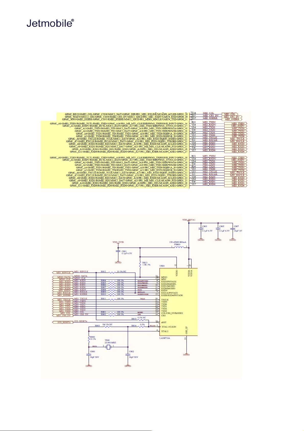
5.8.1 Ethernet Processor Interface
The connections between the processor and the PHY. The interface is in the MII mode of
operation.
29/51
(c)2014 Jetmobile Pte Ltd
Illustration 12: AM335x RGMII interfaces
Illustration 13: PHY1 Interface

"SecureJet Intelligent Appliance 8.1 - COMPANY CONFIDENTIAL"
Ref. SIA8.1_SRM Rev. B 1.0.0
30/51
(c)2014 Jetmobile Pte Ltd
Illustration 14: PHY2 Interface

"SecureJet Intelligent Appliance 8.1 - COMPANY CONFIDENTIAL"
Ref. SIA8.1_SRM Rev. B 1.0.0
5.8.2 Ethernet Connector Interface
5.8.3 Ethernet PHY Power, Reset, and Clocks
The power, reset, and lock connections to the LAN8710A PHY are illustrated in illustration
14.
5.8.3.1 VDD_3V3B Rail
The VDD_3V3B rail is the main power rail for the LAN8710A. It originates at the VD_3V3B regulator and
is the primary rail that supports all of the peripherals on the board. This rail also supplies the VDDIO rails
which set the voltage levels for all of the I/O signals between the processor and the LAN8710A.
5.8.3.2 VDD_PHYA Rail
A filtered version of VDD_3V3B rail is connected to the VDD rails of the LAN8710 and the termination
resistors on the Ethernet signals. It is labeled as VDD_PHYA. The filtering inductor helps block transients
that may be seen on the VDD_3V3B rail.
5.8.3.3 PHY_VDDCR Rail
The PHY_VDDCR rail originates inside the LAN8710A. Filter and bypass capacitors are used to
filter the rail. Only circuitry inside the LAN8710A uses this rail.
31/51
(c)2014 Jetmobile Pte Ltd
Illustration 15: Ethernet Connector Interface

"SecureJet Intelligent Appliance 8.1 - COMPANY CONFIDENTIAL"
Ref. SIA8.1_SRM Rev. B 1.0.0
5.8.3.4 SYS_RESET
The reset of the LAN8710A is controlled via the SYS_RESETn signal, the main board reset
line.
5.8.3.5 Clock Signals
A crystal is used to create the clock for the LAN8710A. The processor uses the RMII_RXCLK
signal to provide the clocking for the data between the processor and the LAN8710A.
5.8.4 LAN8710A Mode Pins
There are mode pins on the LAN8710A that sets the operational mode for the PHY when
coming out of reset. These signals are also used to communicate between the processor and
the LAN8710A. As a result, these signals can be driven by the processor which can cause the
PHY not to be initiated correctly. To ensure that this does not happen, three low value pull up
resistors are used.
This will set the mode to be 111, which enables all modes and enables auto-negotiation.
32/51
(c)2014 Jetmobile Pte Ltd
Illustration 16: PHY pin modes

"SecureJet Intelligent Appliance 8.1 - COMPANY CONFIDENTIAL"
Ref. SIA8.1_SRM Rev. B 1.0.0
5.9 USB Host
The board is equipped with a single USB host interface accessible from a single USB
Type A female connector. The design of the USB Host circuitry (extract from schematic page 4).
5.9.1 Power Switch
U401 is a switch that allows the power to the connector to be turned on or off by the
processor. It also has an over current detection that can alert the processor if the current gets
too high via the USB1_OC signal. The power is controlled by the USB1_DRVBUS signal from
the processor.
5.9.2 ESD Protection
U403 is the ESD protection for the signals that go to the connector.
5.9.3 Filter Options
FB400 and FB401 were added to assist in passing the FCC emissions test. The USB1_VBUS
signal is used by the processor to detect that the 5V is present on the connector.
33/51
(c)2014 Jetmobile Pte Ltd
Illustration 17: USB Host

"SecureJet Intelligent Appliance 8.1 - COMPANY CONFIDENTIAL"
Ref. SIA8.1_SRM Rev. B 1.0.0
6 CONNECTORS
Each board has a debug serial interface that can be accessed by using a special serial cable
that is plugged into the serial header.
Two signals are provided, TX and RX on this connector. The levels on these signals are 3.3V. In
order to access these signals, a FTDI USB to Serial cable is recommended as shown in Figure
below.
The cable can be purchased from several different places and must be the 3.3V version TTL232R-3V3. Information on the cable itself can be found direct from FTDI at:
http://www.ftdichip.com/Support/Documents/DataSheets/Cables/DS_TTL-232R_CABLES.pdf
34/51
(c)2014 Jetmobile Pte Ltd

FCC NOTE:
This equipment has been tested and found to comply with the limits for a Class B
digital device, pursuant to part 15 of the FCC Rules. These limits are designed to
provide reasonable protection against harmful interference in a residential
installation. This equipment generates, uses and can radiate radio frequency energy
and, if not installed and used in accordance with the instructions, may cause harmful
interference to radio communications. However, there is no guarantee that
interference will not occur in a particular installation. If this equipment does cause
harmful interference to radio or television reception, which can be determined by
turning the equipment off and on, the user is encouraged to try to correct the
interference by one or more of the following measures:
Reorient or relocate the receiving antenna.
Increase the separation between the equipment and receiver.
Connect the equipment into an outlet on a circuit different from that to
which the receiver is connected.
Consult the dealer or an experienced radio/TV technician for help.
Caution: Any changes or modifications to this device not explicitly approved by
manufacturer could void your authority to operate this equipment.
This device complies with part 15 of the FCC Rules. Operation is subject to the
following two conditions: (1) This device may not cause harmful interference, and (2)
this device must accept any interference received, including interference that may
cause undesired operation.
 Loading...