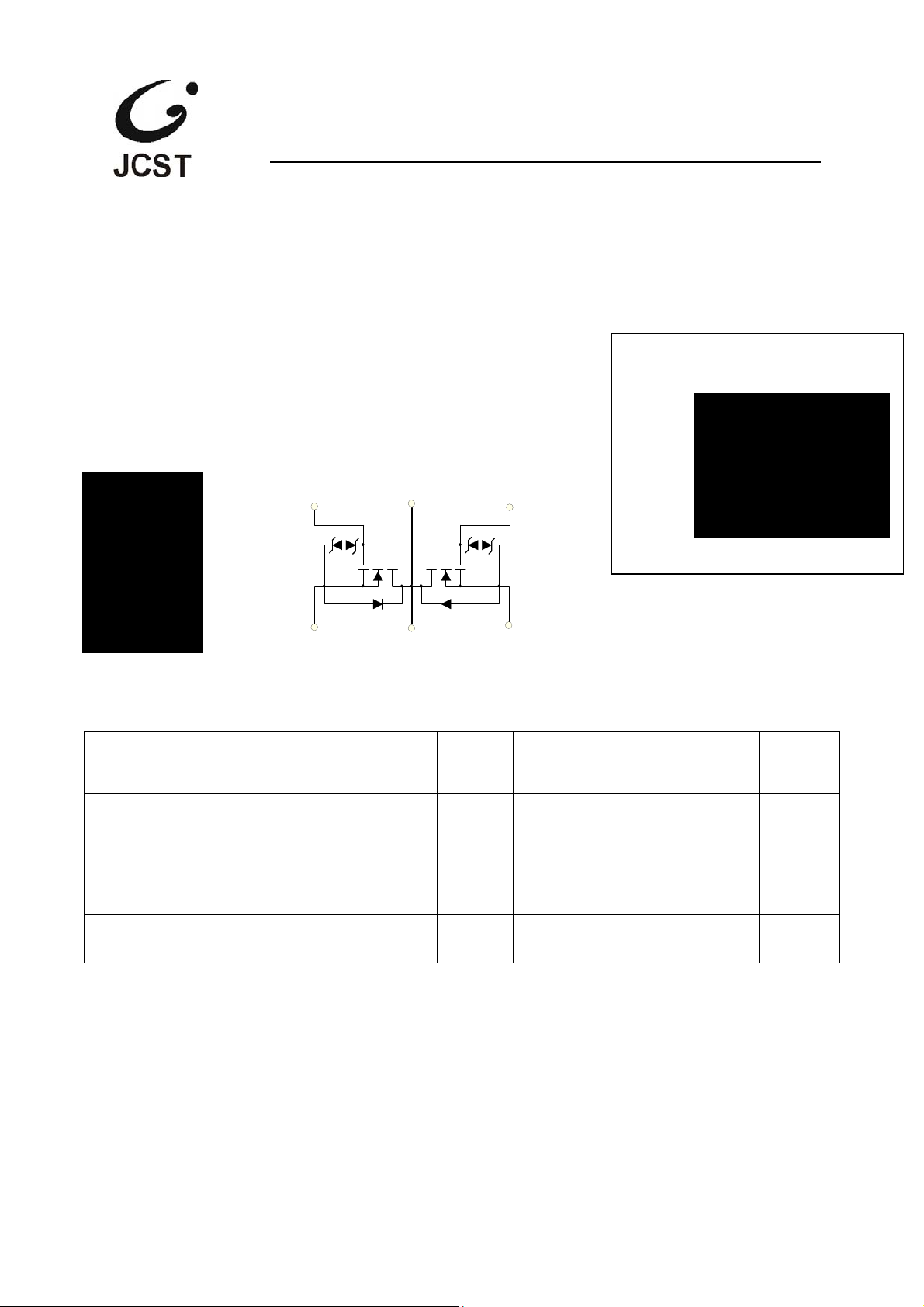
JCST CJL8820 Schematic [ru]

C,Dec,2013
JIANGSU CHANGJIANG ELECTRONICS TECHNOLOGY CO., LTD
SOT-23-6L Plastic-Encapsulate MOSFETS
CJL8820 Dual N-Channel Enhancement Mode Field Effect Transistor
DESCRIPTION
The CJL8820 use advanced trench technology to provide excellent
R
and low gate charge. It is ESD protected. This device is suitable
DS(ON)
for use as a uni-directional or bi-directional load switch,facilitated by its
common-drain configuration.
6
G1
D1,2
5
4
G2
SOT-23-6L
3
S2
25 A
DM
125
JA
-55~ +150
stg
℃/W
℃
℃
1
S1
2
D1,2
ABSOLUTE MAXIMUM RATINGS (T
Parameter Symbol Value Unit
Drain-source voltage VDS 20 V
Gate-source voltage VGS ±12 V
Continuous drain current (t 10s) ID 7 A
Pulsed drain current * I
Power dissipation* PD 1 W
Thermal resistance from junction to ambient R
Junction temperature TJ 150
Storage temperature T
=25℃ unless otherwise noted)
a
* Repetitive rating : Pulse width limited by junction temperature.

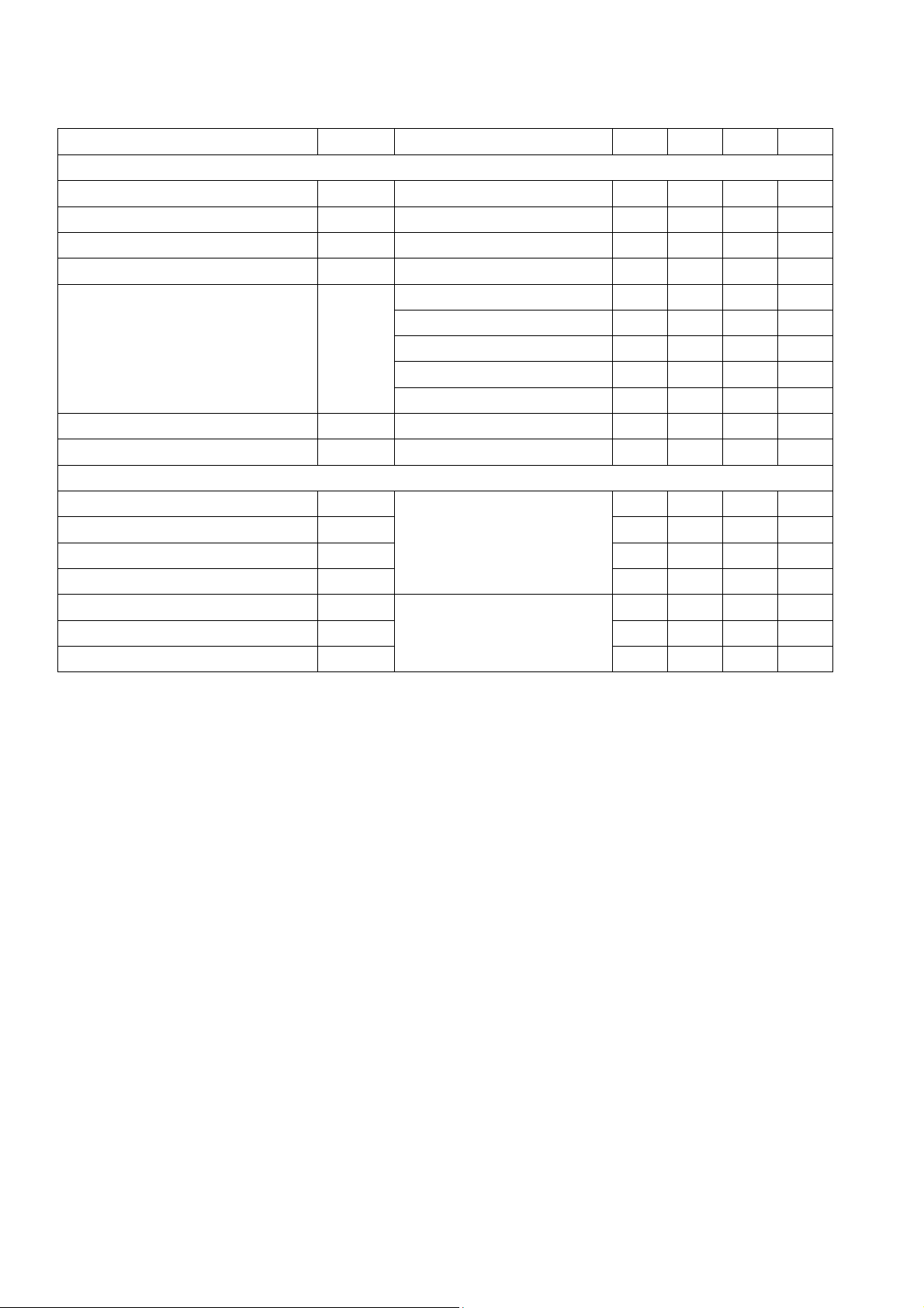
ELECTRICAL CHARACTERISTICS (T
C,Dec,2013
Parameter Symbol Test Condition Min Typ Max Unit
STATIC PARAMETERS
Drain-source breakdown voltage V (BR) DSS VGS = 0V, ID =250µA 20
Zero gate voltage drain current IDSS VDS =16V,VGS = 0V
Gate-body leakage current IGSS VGS =±10V, VDS = 0V
Gate threshold voltage (note 1) VGS(th) VDS =VGS, ID =250µA 0.5
Drain-source on-resistance (note 1) RDS(on)
Forward tranconductance (note 1) gFS VDS =5V, ID =7A
Diode forward voltage(note 1) V
SWITCHING PARAMETERS(note 2)
Turn-on delay time td(on)
Turn-on rise time tr
Turn-off delay time td(off)
Turn-off fall time tf
Total Gate Charge Qg
Gate-Source Charge Qgs
Gate-Drain Charge Qgd
Notes :
1. Pulse Test : Pulse width300µs, duty cycle0.5%.
2. Guaranteed by design, not subject to production testing.
=25℃ unless otherwise noted)
a
VGS =10V, ID =7A
VGS =4.5V, ID =6.6A
VGS =3.8V, ID =6A
VGS =2.5V, ID =5.5A
VGS =1.8V, ID =2A
IS=1A, VGS = 0V
SD
VGS=5V,VDS=10V,
R
=1.4,R
L
DS =10V,VGS =4.5V,ID =7A
V
GEN
=3
9
1 µA
±10 µA
1.1 V
21 m
24 m
28 m
32 m
50 m
1 ns
1 ns
8 ns
18 ns
9
2
1
1
V
S
V
nC
nC
nC
 Loading...