

Page 1
1
ELECTRONIC CASH REGISTER
J3500E
SERVICE MANUAL
DOCUMENT No. 5190-02-03
REV.01
TITLE : J3500E SERVICE MANUAL
DRAW CHECK APPR.
PREPARED BY K. SAKAUE 2004/12/6
APPROVED BY
COPY RIGHT 2004 BY JAPAN CASH MACHINE CO., LTD.
Page 2

2
TABLE OF CONTENTS
1 Introduction..................................................................................................................................................................1
2 Installation procedure..................................................................................................................................................1
2.1 unpacking ..............................................................................................................................................................1
2.2 Emergency cash drawer release...........................................................................................................................2
2.3 Preparation for use .............................................................................................................................................2
Dip switch setting....................................................................................................................................................2
Initial reset procedure.............................................................................................................................................2
Diagnostics...............................................................................................................................................................3
3 Theory of operation ......................................................................................................................................................4
3.1 system block diagram............................................................................................................................................4
3.2 circuit description..................................................................................................................................................5
3.2.1 power circuit ...................................................................................................................................................5
3.2.2 PF CIRCUIT ...................................................................................................................................................6
3.2.3 KEY BOARD CIRCUIT..................................................................................................................................7
3.2.4. display circuit ................................................................................................................................................8
3.2.5. printer drive circuit .......................................................................................................................................9
3.2.6. Comparator circuit ........................................................................................................................................9
3.2.7. Motor drive circuit(paper feed motor) ........................................................................................................10
4 Trouble shooting ...................................................................................................................................................... 11
5 CONNECTOR LAYOUT .........................................................................................................................................13
5.1 CONNECTOR TABLE......................................................................................................................................14
5.2 Standard inner cable pin assignment ................................................................................................................16
5.3 Optional cable pin assignment ...........................................................................................................................16
6 Appendix .....................................................................................................................................................................17
Revision table ................................................................................................................................................................18
Page 3

1
1 Introduction
J3500E consist of 5 block
(1)Main CPU board
Main CPU:M16C/80 Renesas device 16 bit MPU
RAM 4M bit (battery back up)
EPROM 4M bit CMOS
(2) Front display unit
(3) Rear display unit
(4) Key board unit
(5) Power supply unit
2 Installation procedure
2.1 unpacking
The ECR packing method is shown fig 2-1.
Unpack the ECR an check that the following items are present.
(1) One roll of thermal rolls 58mm
(2) key set
(3) J3500E owners manual
(4) Dust cover
If the ECR was received in a damaged carton, unpack and inspect for physical damage immediately,
As described in table 2-1. If damage is found, contact the freight carrier and file a claim promptly,.
If any parts are missing, contact JCM within one week of receiving the ECR.
Initial inspection
Perform the appearance and mechanical checks as listed on table 2-1.
The ECR cabinet can be detached by removing the two screw on the back side of the cabinet.
Table 2-1 Check List
Inspection check
Appearance A. surface of cabinet , keyboard, and cash drawer for damage
such as dents and scratches.
B. display windows for damage such as
cracks or scratches.
Mechanical A. all electrical connections for proper seating
B. keys in mode lock for proper operation.
C. Cash drawer for smooth operation when released manually.
See selection 2.3 for release details.
Page 4
2
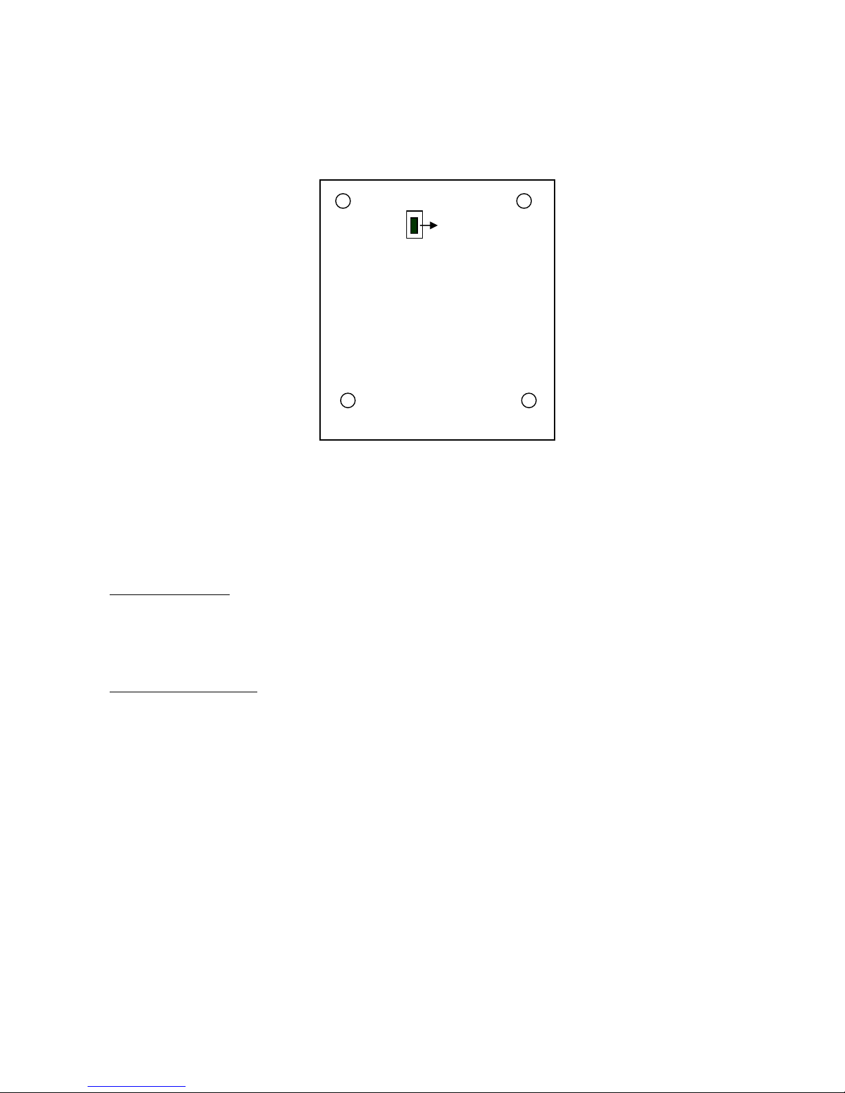
2.2 Emergency cash drawer release
In the unlikely event of a machine malfunction or a prolonged power failure, the model J3500E is
equipped with an emergency cash drawer release.
The release is located on the rear underside of the cash drawer. To manually release the drawer,
carefully lift one side of the ECR with your left hand and push the release tab with the other.
FIGURE 2-2 Emergency Drawer Release
2.3 Preparation for use
Dip switch setting
Dip switch is located on the front center of the main PCB.
It is used for initialization and hardware configuration purposes.
1: ON initial reset
OFF normal operation
Initial reset procedure
(a) Initial reset
(1) set DIP sw1 to ON.
(2) Power ON.
Clears RAM work area only (current transaction)
Does not effect totals/counters or program memory.
Operation mode become “P” mode.
(b) RAM clear(all clear)
(1) Turn the mode lock key to the “P”mode.
(2) Set DIP sw1 to ON
(3) Power ON while depressing the tenkey ”1”.
(4) All clear is displayed.
Clears all Totals/counters and user programmed memory. Loads default operation program
After all clear operation, you must preset the date and time in “X” mode.
The machine does not work without setting date and time.
Rear
BOTTOM VIEW
FRONT
release
Page 5

3
Diagnostics
(1) turn the mode lock key to “P” position, or assign to “P” mode(4---key).
(2) Enter xxxxxxxxx(9digit) --- #/NS
555555555-----#/NS automatic receipt issue at 3 minutes interval.
555555551-----#/NS automatic receipt issue at 5 second interval without cutter.
555555552-----#/NS automatic receipt issue at 5 seconds interval with cutter.
666666666-----#/NS communication port loop back test
check the com. Port from 1 to 3.
Following result message is printed
Error2 RTS---CTS defect
Error4 RxD ---TxD defect
777777777-----#/NS automatic printing test
All characters are printed on receipt automatically.
You can do a check of printing quality.
It’s terminated by depressing “CL” key
888888888-----#/NS key board test
the display will show the each key’s position number on the right side 2 digit
various signal status will be showed each digit on the display.
It’s terminated by depressing “CASH” key.
For example(display)
P
1 0 1 4 5
Key position code
Blank area
Receipt paper empty
Head up switch
Control key position
999999999-----#/NS version and check sum display
The software version number and checksum of EP-ROM will displayed.
For example(display)
1 - 0 0
E F 1 0 3
check sum
destination spec.
Version number
Page 6

4
Section 2
3 Theory of operation
3.1 system block diagram
SCOM3 is reserved
The ECR circuitry can be broken down into six major sections: MPU, Memory, Display,
Key board, Printer, and power supply.
The heart of this system consists of a M16C/80, Sixteen bit microprocessor
implementing L.S.I, high speed, and low power consumption.
Standard memory includes a 512k x 8 bit EPROM and a 512k x 8 bit static RAM chip.
Printer unit
GTP58
With auto cutter
Front display
9 digit(LED)
SCOM1 SCOM2
Rear display
9 digits(LED)
MPU
M16C/80
E-PROM’(4M)
4M
RAM
232C DRIVER
KEY BOARD
9 X 8 MATRIX
CONTROL LOCK
PRINTER
DRIVER
CIRCUIT
DRAWER
DRAWER
DRIVER
POWER
CIRCUIT
LED driver
(digit)
SCOM3
SWITCHING
POWER SUPPLY
(+24V)
MAIN
LED driver
(segment)
Page 7

5
C46
104C
1011
U12E
SN74LV14APW_VBB
+-
BT1
3/V 280R
R5
122
R43
103
1
TP2
TEST POINT
1
TP3
TEST POINT
R42
103
C47
104C
R44
103
1011
U10E
SN74LV14APW
1213
U12F
SN74LV14APW_VBB
1
2
3
4
CN2
B4P-VH
D2
HZU15B2
VOUT
1
MNURST
2
VCC
3
GND
4
U9
PST591CMT
1213
U10F
SN74LV14APW
C3
104C
R3
122
D3
HZU4.3B2
1
TP1
TEST POINT
nPF
nRESET
VCC
+24V
+24V
VCCVCC
VBB5 VBB5
nRESET-VBB
89
U12D
SN74LV14APW_VBB
65
U12C
SN74LV14APW_VBB
VBB5 VBB5
VOUT1VIN
2
CB
3
FB
6
NC5GND4ON/OFF
7
U1
LM2676S-5.0
C5
103C
D4
EC31QS06
C6
UPW1H471MHH
C7
UPW1V471MPH
L1
SLF12565T-470M2R4
R11
561
R10
221R9OPEN
VOUT8VIN
7
CB
1
FB
4
NC2GND
6
ON/OFF
5
NC
3
U2
LM2675M-5.0
C9
103C
D7
EC31QS06
C8
UPW1H471MHH
C13
UPW1V101MPH
+5VSUB
D6
CMS06
D5
CMS06
R8
100
C4
16V100u LL
VBB
VCC
C10
16V100u LL
RESET-VBB
FL1
DSS9ND31H223
FB5
BLM21PG600SN1
L2
SLF12565T-470M2R4
89
U10D
SN74LV14APW
43
U10B
SN74LV14APW
65
U10C
SN74LV14APW
21
U10A
SN74LV14APW
43
U12B
SN74LV14APW_VBB
3.2 circuit description
3.2.1 power circuit
After passing through the switching regulator. There is a +24V DC power via CN2.
+24V power is supplied to printer circuit. On the other hand, it’s supplied to regulator
circuit too. There are two regulator circuit.
U1(LM2676S-5.0) is used for logic circuit and for memory back up circuit.
+24V pass through U1(LM2676S-5.0) becomes +5V steady.
During normal operation, the voltage of Vbb line is supplied by +5V line.
Rechargeable current is applied to rechargeable battery via R8.
When AC power is removed, the +5V line decreases, and D5 is turn OFF.
Then the battery supplies Vbb line. And back up the memory contents of RAM chip and CPU
Internal RAM
D5 is used to avoid reverse current when power OFF.
U2(LM2675M-5.0) is used for communication circuit.
+24V pass through U2(LM2675M-5.0) become +5V steady.
Page 8

6
3.2.2 PF CIRCUIT
Power ON
When AC input turn ON, the level of U12-11 rise up to +4.3V.
When input voltage of U12-11 become 3.3V, the output of U12-12(nPF) turn “H”.
Then system goes to operation mode.
Power OFF
When AC input turn OFF, the level of U12-11 fall to 0V.
When input voltage of U12-11 become 2.2V, the output of U12-12(nPF) turn “L”.
Then system goes to standby mode.
+21.6V 24.4V
19.6V
PF signal
+5V
PF signal timing chart
Page 9

7
KR0
1
KR1
2
KR2
3
KR3
4
KR4
5
CN13
W-D0805#01
KS0
1
KS1
2
KS2
3
KS3
4
KS4
5
KS5
6
KS6
7
KS7
8
KS8
9
CN15
W-D0809#01
COM
1
REG
2
X
3
Z
4
P
5
SP
6
CN14
5267-06A
KS[0..3]
KEY SCAN
KEY RETURN
CONTROL
A
1
B
2
C
3
G1
6
G2A
4
G2B
5
Y0
15
Y1
14
Y2
13
Y3
12
Y4
11
Y5
10
Y6
9
Y7
7
U22
SN74LV138APWR
A
1
B
2
C
3
G1
6
G2A
4
G2B
5
Y0
15
Y1
14
Y2
13
Y3
12
Y4
11
Y5
10
Y6
9
Y7
7
U21
SN74LV138APWR
D23 1SS355
D14 1SS355
D20 1SS355
D15 1SS355
D21 1SS355
D16 1SS355
D22 1SS355
D17 1SS355
D18
1SS355
D19
1SS355
VCC
FB75 BLM21AG121SN1
FB76 BLM21AG121SN1
FB77 BLM21AG121SN1
FB78 BLM21AG121SN1
FB79 BLM21AG121SN1
FB80 BLM21AG121SN1
FB81 BLM21AG121SN1
FB82 BLM21AG121SN1
FB83 BLM21AG121SN1
FB64 BLM21AG121SN1
FB66 BLM21AG121SN1
FB68 BLM21AG121SN1
FB70 BLM21AG121SN1
FB72 BLM21AG121SN1
FB74 BLM21AG121SN1
FB65 BLM21AG121SN1
FB67 BLM21AG121SN1
FB69 BLM21AG121SN1
FB71 BLM21AG121SN1
FB73 BLM21AG121SN1
1
2
4
3
DSW1
KSD-02
D13
1SS355
D12
1SS355
R68
473
R66
473
R69
473
R67
473
R64
473
C77
101C
C75
101C
C78
101C
C76
101C
C74
101C
KS0
KS1
KS2
KS3
KR[0..4]
KR[0..4]
KR0
KR1
KR2
KR3
KR4
VCC VCC VCC VCC VCC
2345789
1106
RA6
RA104
VCC VCC
R63
104
R65
104
VCC VCC
KS[0..3]
3.2.3 KEY BOARD CIRCUIT
Input and output signal for key board scanning are passing through CN13~CN15.
The output signals from output port (P140-P143) of U11 are encoded signals.
By passing through U21,U22(74HC138), they are decoded to key scan signals. And they are
applied to key matrix via CN15.
When a certain key is depressed, one of decoded signal is applied to U11(MPU) via CN13.
Thus U11(MPU) recognizes which key is depressed and executes key’s specific operation.
The scanning signal from U26 –Y1 scans control lines KR0-KR4 and they are applied to
U11(MPU) as control signals.
According to the status of control signals, U11(MPU) executes specific operation.
Scan signal
MPU
Data bus
Fig 3-1 key board circuit
Timing chart of key scan signals
P140
P141
P142
P143
Y0
Y1
Y2
Y7
5.48msec
Page 10

8
3.2.4. display circuit
Display signals are applied to display circuit board via CN3.
The display signals for digit indication are supplied from P120 to P127 and P145,P146 of CPU ports.
The digit indication signals are amplified at 9 FETs.(2SJ208) And they are supplied to LED common
terminal on FD and supplied to RI ones.
The segment data signals are amplified at U14’(M54583) and supplied to segment line of FD and RI
circuit board.
From CPU
board
segment
signal
for RI
digit signal
for RI
DET1
1
DSP A
2
DSP B
3
DSP C
4
DSP D
5
DSP E
6
DSP F
7
DSP G
8
DSP P
9
DSP G1
10
DSP G2
11
DSP G3
12
DSP G4
13
DSP G5
14
DSP G6
15
DSP G7
16
DSP G8
17
DSP G9
18
DSP G10
19
DET2
20
CN3
52045-2010
1110
2
3
4
5
6
7
8
9
19
18
17
16
15
14
13
12
U14
M54583FP
VCC
VCC
VCC
2345789
1106
RA1
RA103
R7
103R6103
VCC
R39
102
R38
102
R37
102
R36
102
R35
102
R34
102
R33
102
R32
102
R30
102
R29
102
DSPG1
DSPG2
DSPG3
DSPG4
DSPG5
DSPG6
DSPG7
DSPG8
DSPG9
DSPG10
DSPG[1..10]
DSPG[1..10]
FB62 BLM21AG121SN1
FB47 BLM21PG600SN1
FB46 BLM21PG600SN1
FB49 BLM21PG600SN1
FB48 BLM21PG600SN1
FB51 BLM21PG600SN1
FB50 BLM21PG600SN1
FB53 BLM21PG600SN1
FB52 BLM21PG600SN1
FB55 BLM21PG600SN1
FB54 BLM21PG600SN1
FB57 BLM21AG121SN1
FB56 BLM21AG121SN1
FB59 BLM21AG121SN1
FB58 BLM21AG121SN1
FB61 BLM21AG121SN1
FB60 BLM21AG121SN1
FB63 BLM21AG121SN1
DSPS[1..8]
DSPS[1..8]
DSPS1
DSPS2
DSPS3
DSPS4
DSPS5
DSPS6
DSPS7
DSPS8
FB45
BLM21PG600SN1
C54
103C
C52
103C
C48
103C
C63
103C
C26
103C
C62
103C
C73
103C
C72
103C
C70
103C
74LV00A 74LV14A 74LV14A 74LV32A 74LV32A 74LV123A 74LV138A 74LV138A LMV358
C66
103C
LM393
VBB VBB VCC VCC VCC VCC VCC VCC VCC VCC
8PIN
7PIN 7PIN 7PIN 7PIN 7PIN 8PIN 8PIN 8PIN 4PIN
8PIN
4PIN
16PIN 16PIN16PIN14PIN 14PIN14PIN14PIN14PIN
2
13
Q14
2SJ208
2
13
Q6
2SJ208
2
13
Q13
2SJ208
2
13
Q5
2SJ208
2
13
Q12
2SJ208
2
13
Q4
2SJ208
2
13
Q11
2SJ208
2
13
Q3
2SJ208
2
13
Q10
2SJ208
2
13
Q2
2SJ208
Page 11

9
G
D
S
Q8
2SK2569
R
CX
RX/CX
&
1
2
3
14
15
4
13
U16A
SN74LV123APW
S
2
D
6
D
7
S
3
G
4
S
1
D
5
D
8
Q9
IRF7424
D25
1SS226
R52 153
C69
104C
R57 472
1
2
3
U5A
SN74LV32APW
-
+
3
2
1
U19A
LM393M
R14
472
R60
103
R
CX
RX/CX
&
9
10
11
6
7
12
5
U16B
SN74LV123APW
R58
222
C28
101C
R53
473
9
10
8
U5C
SN74LV32APW
C61
35V 1000u
R54
103
C25
471C
R12
472
-
+
5
6
7
U19B
LM393M
12
13
11
U5D
SN74LV32APW
R51
103
R50
103
4
5
6
U5B
SN74LV32APW
C64
104F
C35
471C
R56
472
R49
103
C33
101C
R13
103
C23
471C
PRI_EN
PRSTB1
PRSTB2
TH
PR/LAT0
PRCLK0
PRDIO
nRESET
VCC
VCC
+24V
VCC
VCC VCC VCC
VCC
VCC
TH
TH
VH
28
VH
27
TM1
19
TM2
9
DO
24
GND
18
GND
17
GND
16
GND
15
VDD
8
/STB3
7
/LAT
22
CLK
23
/STB2
6
VH
4
VH
3
VH
26
VH
25
VH
2
VH
1
DI
5
NC
21
/STB1
20
GND
14
GND
13
GND
12
GND
11
GND
10
CN7
28FE
VCC
1
2 12
13
U17A
SN74LV10APW
PRSTB3
FB28
BLM21AG121SN1
FB31
BLM21AG121SN1
FB29
BLM21AG121SN1
C29
101C
4
5
6
U15B
SN74LV32APW
12
13
11
U15D
SN74LV32APW
1
2
3
U15A
SN74LV32APW
9
10
8
U15C
SN74LV32APW
FB26 BLM21AG121SN1
FB27 BLM21AG121SN1
FB32 BLM21AG121SN1
FB30
BLM21PG600SN1
C32
104C
C60
35V 1000u
C30
50V 10u
C27
50V 10u
C22
50V 10u
C24
50V 10u
4
5
6
3
U17B
SN74LV10APW
9
10 8
11
U17C
SN74LV10APW
3.2.5. printer drive circuit
Printer drive circuit consists of U11(MPU), U15,U16,U17 and U18 (driver), U19 (comparator)
Usually, P73 outputs “L” level. When one of department key is depressed, CPU outputs printer power
Signal “H”(PRI_EN) from output port P73 of U11. Q8and Q9 turn ON. Thus the thermal head
On the printer mechanism is activated.
Serial print data input from “PRDIO” is transferred to the shift register synchronously with the
Clock ”PR_CLK0”, then stored in the latch register at the timing of the latch ”PR/LAT0” signal.
The heat elements which correspond to the latched print data are activated while each gate is on.
The gates are on while each head activation signal (PRSTB1-PRSTB3) is low.
3.2.6. Comparator circuit
The thermal head has a thermistor for detect the head temperature.
The level of the “TH” is changed according to head temperature.
When head is heated too high temperature, the output level of comparator goes to “H” level.
Thus thermal head will be non-activity.
This status is released when the head become cool.
Page 12

10
F2
CCP2E25
PH1
PH2
DA0
+24V
OUT1A
17
OUT2A
20
OUT1B
14
OUT2B
23
VCC
8
VBB
24
VREF1
10
VREF2
4
GND
6
GND
7
GND
18
GND
19
RC2
5
RC1
9
SENSE1
15
E1
16
SENCE2
22
E2
21
PHASE1
11
PHASE2
3
I01
13
I02
1
I11
12
I12
2
U18
UDN2916LB
1B
3
1A
1
2B
4
2A
2
M
CN8
B04B-PASK-1
-
+
3
2
1
U20A
LMV358M
R59
563
R55
563
R18
102
R15
102
R17
1W 0R82
R16
1W 0R82
C36
471C
C34
471C
C67
471C
C68
471C
R62
106
R61
OPEN
FB36 BLM21PG600SN1
FB34 BLM21PG600SN1
FB35 BLM21PG600SN1
FB33 BLM21PG600SN1
C31
50V100u
C65
104C
VCC
MOT_I0
MOT_I1
D8
SS16D9SS16
D10
SS16
D11
SS16
3.2.7. Motor drive circuit(paper feed motor)
After PF_I0,PF_I1 set to “L” level, the signal PF_PH1,PF_PH2 are sequentially changed
for to feed the receipt paper. Similarly after JF_I0,JF_I1 set to “L” level, the signal JF_PH1,
JF_PH2 are sequentially changed for to feed the journal paper.
Page 13

11
+
4 Trouble shooting
Phenomenon condition Considerable cause Check point/method Remedy
AC power is not supplied
AC power is not applied to
switching power supply.
Is AC power plug connected to outlet?
Is outlet voltage normal?
Is fuse (primary side of switching
Power supply?
Is 24V output from secondary side of
switching power supply?
Connect the plug to outlet.
Replace the fuse
Replace the switching power supply.
Is DC power voltage
normal?
+5V is not generated.
Is D6 defect?
Is U1 defect?
Replace D6
Replace U1.
Crystal is not oscillating. Check wave form pin 20 and
Pin 22 of U11(frequency 20MHz)
Replace crystal(x1)
Replace U11
Machine
doesn’t work
at all
Printer doesn’t work
after power on
The levels of PF lines don’t
become “H”
Is D2 defect?(open)
Is U12 defect?
Is D3 defect?(short)
Replace D2
Replace U12
Replace D3
Date/time
data fails.
Date doesn’t
increment.
Date /time data
doesn’t increment
correctly
Crystal(x2:32.768kHz) is
not oscillating properly.
Check wave form of pin 17 and pin 18 of
U11(frequency:32.768kHz)
Replace crystal(X2)
Buzzer
doesn’t sound
Trouble in buzzer circuit. When pin 10(P144)of U11 output “H”,
buzzer is driven.
Is Q7 defect?.
Replace the buzzer.
Replace Q7
Drawer is not
opened
Drawer solenoid
doesn’t operate.
Trouble in drawer circuit When pin 114(P114)of U11 output “H”,
drawer solenoid is driven.
Is Q1 defect?.
Replace Q1
Abnormal
print out
Printed character is
Not desired.
The level of thermister
signal is not stable.
Printer is defect.
Is the signal level of pin 1(U19) stable? Replace U19
Replace printer
Page 14

12
PHENOMEN
ON
CONDITION CONSIDERABLE
CAUSE
CHECK POINT/
METHOD
REMEDY
Is the head unit over heat? When the head is over heated, printing is
stop.
Wait for head becomes cool.
Printer
doesn’t work
at all
Printer motor doesn’t
rotate
Stepping signal does not
generated.
Is the stepping signal output from
P11X(U11)?
Is the stepping signal output from U18
Replace U11
Replace U18
Printer feed
the paper
without
printing
Printer motor does
work correctly
DC power for print head
unit is not output
When pin12(P142) of U11 outputs “H” ,
the head become active.
Replace Q3,Q4.
The FPC for CPU and FD
units connection is broken
Check conduction of FPC. Replace FPC
Segment signal is not
generated
Is U14 defect? Replace U14
Check the voltage between VF1 and
VF2(tolerance3.46Vrms)
Replace converter transformer
Is the cathode voltage of PD14-23.5V? Replace PD14.
Abnormal
display
Display doesn’t light
Display PCB is broken. Is the display PCB cracked? Replace the display unit
Specific digit
is not lit
correctly
Key input correct Trouble in FD digit driver. Check the condition of the FPC
Check the FET of digit driver.
Replace FPC
Replace FET(Q2~Q6,Q10~Q14
Specific
segment is
not lit
correctly
Display data and time
data are correct.
Trouble in segment drive. Check the condition of the FPC.
Check the output of U14
Replace FPC
Replace U14
2 key are depressed
together
Check whethe r any key keeps depressing. Replace key board unit.
Control mode is lock
position
When control lock is released, lock signal
is applied to KR lines(KR0-KR4)
Replace D10
Check conduction of the control key.
Diodes (D14-D23)
are defect.
Check the diode on the output line of
specific key’s key matrix.
Check diode on key
Matrix output.
Key input
cannot be
accepted
Specific key input
cannot be accepted.
Key depressing section is
defect.
Replace key depressing section
Page 15

13
5 CONNECTOR LAYOUT
OF CPU BOARD
CN4CN5CN6
CN17
CN16
CN15
CN13
CN14
CN3
CN11CN10
CN9
CN8
CN7
PRO M
RAM
CPU
CN2
BATT
CN1
CN12
1 2
PRINT HEAD
MOTOR
SCO M 0
SCOM 1
SCO M 2
DISPLAY
PO WER
DRW
Page 16

14
5.1 CONNECTOR TABLE
CN1 CN2 CN4 CN5 CN6
DRAWER POWER SCOM0 SCOM1 SCOM2
PIN signal PIN signal PIN signal PIN signal PIN signal
1 +24V 1 GND 1 SG 1 SG 1 SG
2 DRW 2 GND 2 TxD 2 TxD 2 TxD
3 DRW SOL 3 +24V 3 RxD 3 RxD 3 RxD
4 SG 4 +24V 4 RTS 4 RTS 4 RTS
5 CTS 5 CTS 5 CTS
6 Vcc 6 DTR 6 DTR
7 DSR 7 DSR
CN3 CN8 CN9 CN10
display MOTOR Paper end Head up SW
PIN signal PIN signal PIN signal PIN PIN signal
1 DET1 11 DSP G2 1 1A 1 LED 1 HS
2 DSP A 12 DSP G3 2 2A 2 SG 2 SG
3 DSP B 13 DSP G4 3 1B 3 NEND 3 NC
4 DSP C 14 DSP G5 4 2B 4 SG
5 DSP D 15 DSP G6 CN13
6 DSP E 16 DSP G7 CN11 CN12 key return
7 DSP F 17 DSP G8 CUTTER SW Paper NEND PIN signal
8 DSP G 18 DSP G9 PIN signal PIN signal 1 KR0
9 DSP P 19 DSP G10 1 CTSW 1 LED 2 KR1
10 DSP G1 20 DET2 2 SG 2 SG 3 KR2
3 NEND 4 KR3
5 KR4
CN7
HEAD CN14 CN15 CN16
PIN signal PIN signal control lock key scan down load
1 VH 15 GND PIN signal PIN signal PIN signal
2 VH 16 GND 1 COM 1 KS0 1 Vcc
3 VH 17 GND 2 REG 2 KS1 2 BUSY
4 VH 18 GND 3 X 3 KS2 3 CLK1
5 DI 19 TM1 4 Z 4 KS3 4 RxD1
6 /STB2 20 /STB1 5 P 5 KS4 5 CE
7 /STB3 21 NC 6 SP 6 KS5 6 EPM
8 VDD 22 /LAT 7 KS6 7 GND
9 TM2 23 CLK 8 KS7 8 RESET
10 GND 24 DO 9 KS8 9 CNVSS
11 GND 25 VH 10 TxD1
12 GND 26 VH
13 GND 27 VH
14 GND 28 VH
Page 17

15
CONNECTOR TABLE (continued)
CN17
3rd DISPLAY
PIN Signal
1 GND
2 Vcc
3 NC
4 L RS
5 L WR
6 L RD
7 L DB0
8 L DB1
9 L DB2
10 L DB3
11 L DB4
12 L DB5
13 L DB6
14 L DB7
Page 18

16
5.2 Standard inner cable pin assignment
COM1 5120-05-03 (for DOS/V pin assign hand scanner)
CN4 signal Direction Dsub 9pin(male) Signal
1 SG GND 5 SG
2 TxD Output 3 TxD
3 RxD Input 2 RxD
4 RTS Output 7 RTS
5 CTS Input 8 CTS
6 Vcc Power 9 Vcc
COM2 5120-05-04 (for DOS/ V PC communication)
CN5 signal Direction Dsub 9pin(male) Signal
1 SG GND 5 SG
2 TxD Output 3 TxD
3 RxD Input 2 RxD
4 RTS Output 7 RTS
5 CTS Input 8 CTS
6 NC
7 NC
8 NC
It can be connected with scanner which have DOS/V pin assign connector directly.
5.3 Optional cable pin assignment
Interface cable for between J3500 and the hand scanner ZE84RMD4JK(Panasonic)
WI-1370
SCOM
side(female)
Signal Dsub 9pin(female) Signal
9 Vcc 9 Vcc
8 CTS 1 CTS
7 RTS 4 RTS
2 RxD 2 RxD
3 TxD 3 TxD
5 GND 7 GND
Interface cable for between J3500 and the GP965
WI-1369
SCOM
side(female)
Signal Dsub 9pin(female) Signal
9 Vcc 6 Vcc
8 CTS 5 CTS
7 RTS 4 RTS
2 RxD 3 RxD
3 TxD 2 TxD
5 GND 1 GND
Application case
1. J3500-----DOS/V scanner
It can be connected directly.
2. J3500-----Panasonic scanner (ZE84RMD4JK)
please use the interface cable WI-1370.
5120-05-03+WI-1370
Page 19

17
3. J3500-----DOS/V PC
It can be connected directly by the cross cable.
4. J3500-----GP965
Case2 : please use the interface cable WI-1369.
5120-05-03+WI-1369 (COM1)
or 5120-05-04+WI-1369 (COM2)
6 Appendix
number of PLU & PB actually maximum occupation.
Standard Memory 256KB Mem. Occ.
PLU 12 char+P-T-D
5349
41 Bytes
PLU 20 char.+P-T-D 4599 49 Bytes
PLU 15 char+stock+P-T-D 4599 49 Bytes
PLU 12 char 6898 30
PLU 20 char 5698 38
PLU 15chrar+stock 5698 38
PB 5698 38 Bytes
Second Lang. The second language have fix
occupation.
16384 Bytes
Electronic journal 5000line x 35 175k Bytes
HARD RESET
It is executed automatically when power is ON.
Page 20

18
Revision table
date description Rev.
Number
Rom ver
2004/12/07 1st edition .01 1.00-3
 Loading...