

Page 1
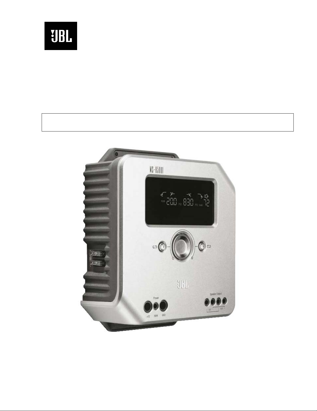
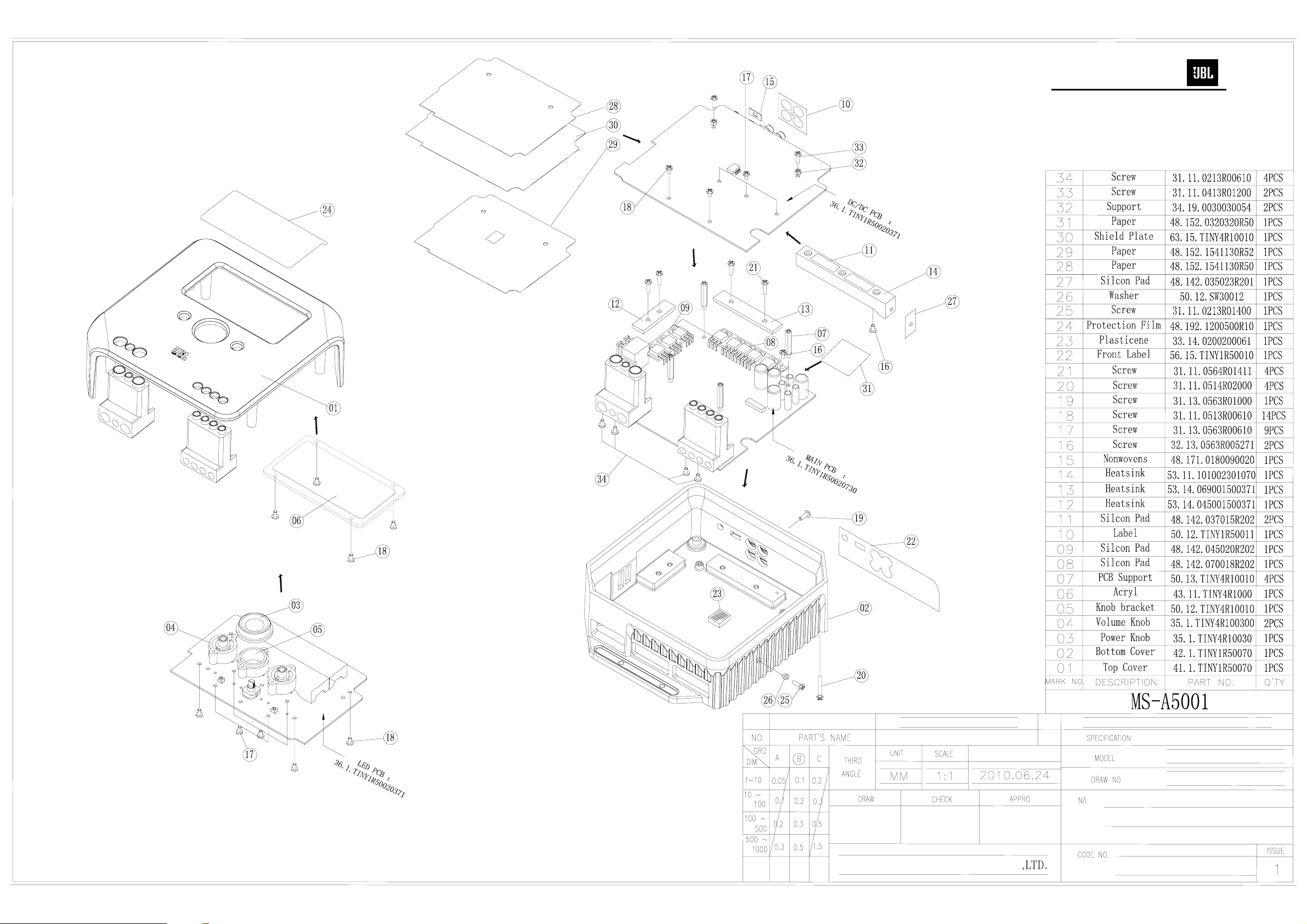
MS-A5001
1 CHANNEL
Digital Signal Processing Amplifier
SERVICE MANUAL
Released 2011
Discontinued XXXX
JBL Consumer Products
8500 Balboa Blvd.
Northridge, CA. 91329 Rev0 8/2011
Page 2

1
MS-A5001
- CONTENTS -
SPECIFICATIONS ………………………………………..1
PACKAGING…………..……………………………..…....2
CONTROL/INSTALLATION DRAWINGS………………3
CONTROL/INSTALLATION INSTRUCTIONS………....4
NOTE ON SETTINGS AND TESTING…..………………5
CONNECTIONS …..………………………………………6
DISPLAY………………………..………………………….9
EXPLODED VIEW/PARTS LIST…….….….……..……10
AMPLIFIER BLOCK DIAGRAMS………………….……11
P.C.B. DRAWINGS….………………………...…….……13
ELECTRICAL PARTS LIST ..……….….…….…….……23
IC/TRANSISTOR PINOUTS..…………………….….…..28
SCHEMATICS……………..………….…….………..…...72
MS-A5001 Specifications
Output Power: 500W RMS x 1 channels @ 4 ohms; ≤1% THD + N
(14.4V supply) 500W RMS x 1 channels @ 2 ohms; ≤1% THD + N
Signal-to-noise ratio: 80dBA (reference 1W into 4 ohms)
106dBA (reference rated power into 4 ohms)
Total Peak power: 500W
Frequency response: 20Hz – 270Hz (–3dB)
THD+N 1KHz LPF=22KHz < 1.0 % (rated power @ 4 ohms)
Input Impedance 10kΩ (Hi2 = 120)
Maximum input signal: 20.0V
Maximum sensitivity: 100mV
Bass Boost @ 80Hz 10dB
DC Offset <50mV
Idle Current @ 4 ohms <1.5A
Max Current Draw ≤45A
Remote Operating Voltage 5-16VDC
Turn-on delay time 1 sec
Circuit Protection
Dimensions: 7-3/16" x 8-1/4" x 2-3/4" 183mm x 210mm x 70mm
Fuse: 2 x 40A
JBL continually strives to update and improve existing products, as well as create new ones. The specifications and details in
this and related JBL publications are therefore subject to change without notice.
Temp (85±5C), Short circuit, Operating voltage range (9-16V)
Page 3
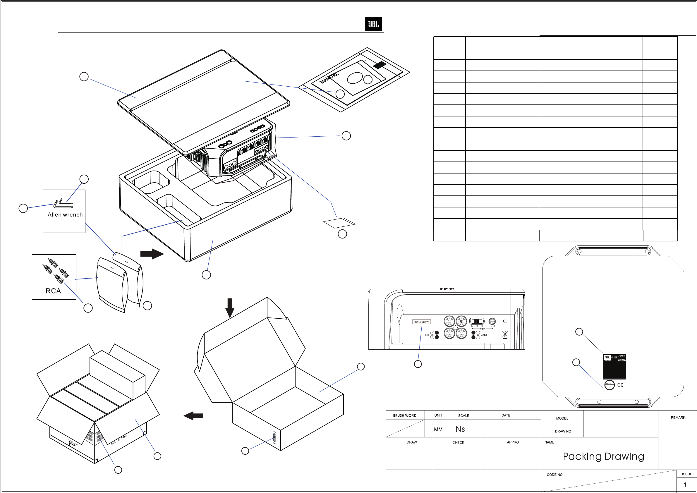
15
14
NO PART NUMBER DESCRIPTION QTY
2
MS-A5001
1 57.12.MS-A10040
2 57.12.TINY4R1000
1
11
3
4 241-59.11.MS-A50010
TOP FOAM PACKAGING
BOTTOM FOAM PACKAGING
SNOW BOX-TOP
SNOW BOX-BOTTON
PLASTIC BAG
OUTER CARTON
GIFT BOX
1
1
1
1
12
MASTER CARTON
5 240-58.11.MS-A50010
6
7 56.13.TINY1R5000
3
8
9 56.18.TINY1R5001
10
11 272-38.112.TINY2
12
visit www.jbl.com
13
14 65.1.2R520 1
15 65.1.0420 1
CARTON BOX
DESICCANT
SERIAL LABEL
GIFT LABEL
CARTON LABEL
CE LABEL
SETUP CD
OWNER'S MANUAL
CD
MANUAL
PLASTIC BAG
2.5mm ALLEN WRENCH
4.0 mm ALLEN WRENCH
1
1
2
1
1
1
1
1
2
16
13
RCA to bare wire Adapters
16 26.121.112101
6
17
56.15.MSA50010
RCA(BLACK) TACK
LABEL
4
1
2
17
4
7
10
Automotive amplifier DC14.4V 80A
FCC ID: TN5MSA5001AS
IC: 6132C-MSA5001AS
This device complies with part 15 of the
FCC Rules. Operation is subject to the
following two conditions:
(1) This device may not cause harmful
interference, and
(2) this device must accept any interference
received, including interference that may
cause undesired operation.
Harman consumer,Inc
Made in China
MADE IN CHINA
5
9
TINY
2010.06.24
8
MP-10D5-0076
Page 4
1
2
Input
1
2
1
2
I
nput
O
utput
Lo
Hi
Hi2
I
nput
L
e
3
MS-A5001
1
3
2
4
1
Lo Hi Hi2
1
Input Output
3
2
Level
Input
1
2
6
40 A
2X40A
40 A
5
9
8
10
11
8
1 x 80A
+
-
10
11
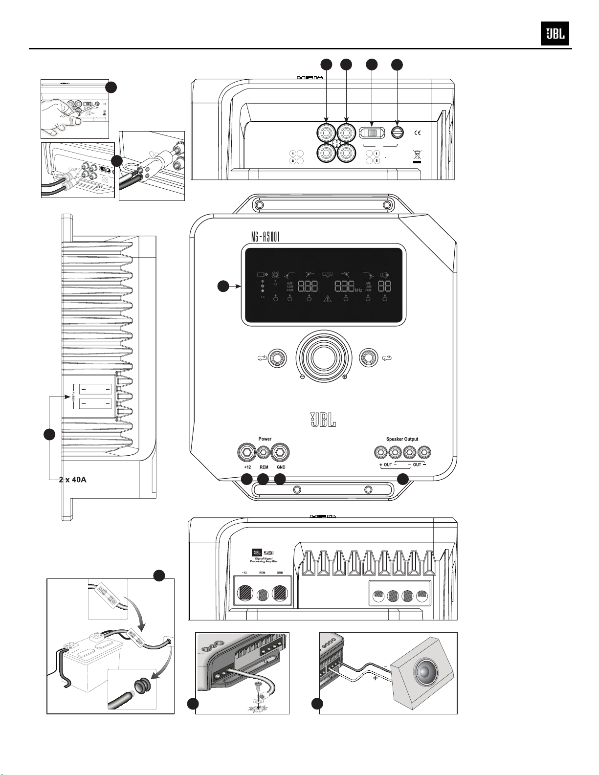
Page 5
4
MS-A5001
1
4
9
5
2
6
3
7
8
10
11
Page 6

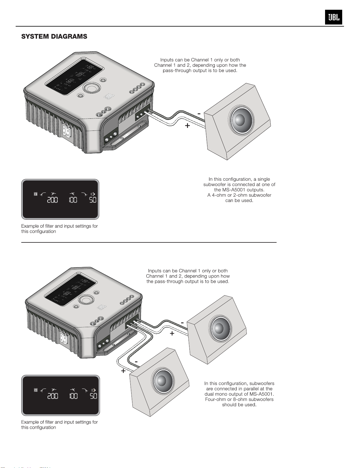
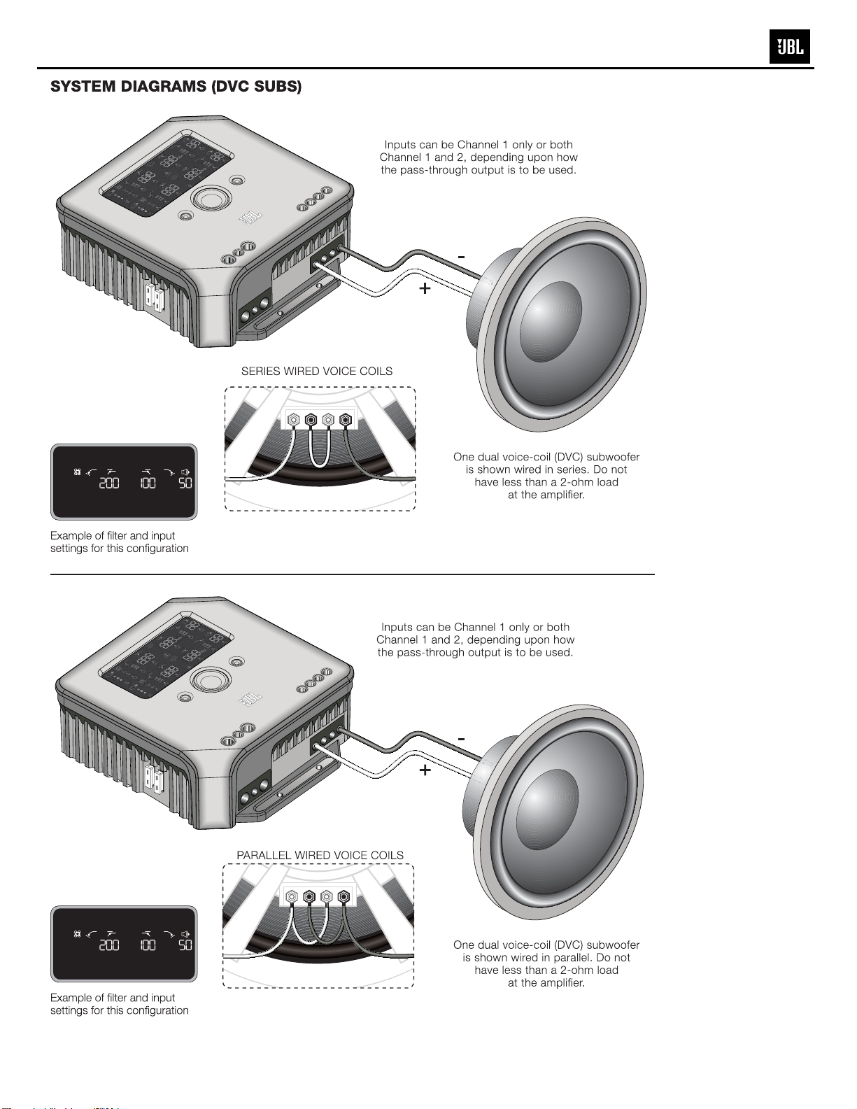
5
MS-A5001
NOTE: Although some typical connections and
®
controls are shown, JBL
MS Series amplifiers
include many features and digital controls not
found on conventional car audio amplifiers.
Also, the setup (or testing) procedure for MS
Series amplifiers is different (more
complicated) from that of conventional car
audio amplifiers.
Details can be found in the MS-A5001 owner’s
manual, which can be downloaded here:
http://www.jbl.com/ENUS/Support/Pages/ProductSelector.aspx
Page 7
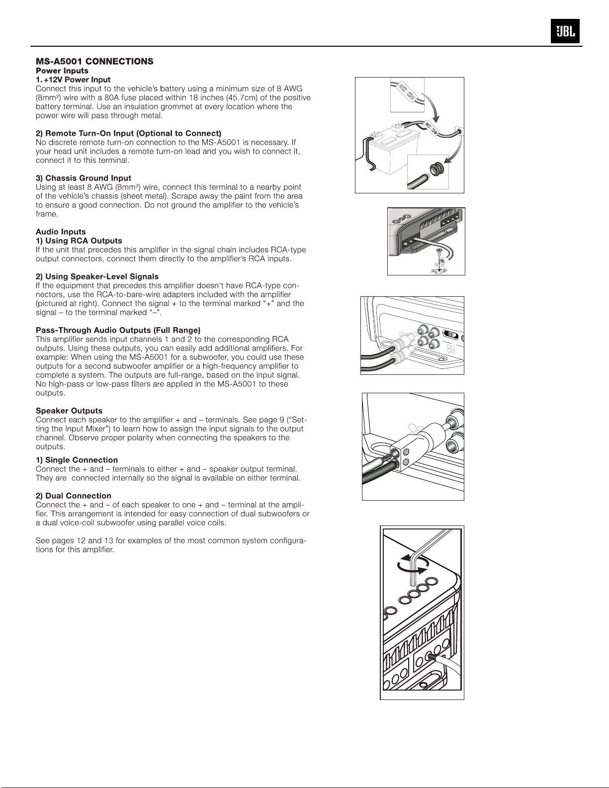
+
-
1 x 80A
1
2
1
2
Input
Output
Lo
Hi
Hi2
Input
L
e
1
2
I
nput
6
MS-A5001
Page 8
7
MS-A5001
1,2
24dB 24dB
1,2
Hz
Hz
1,2
24dB 24dB
1,2
Hz
Hz
Page 9
8
MS-A5001
24dB 24dB
Hz
Hz
24dB 24dB
Hz
Hz
Page 10
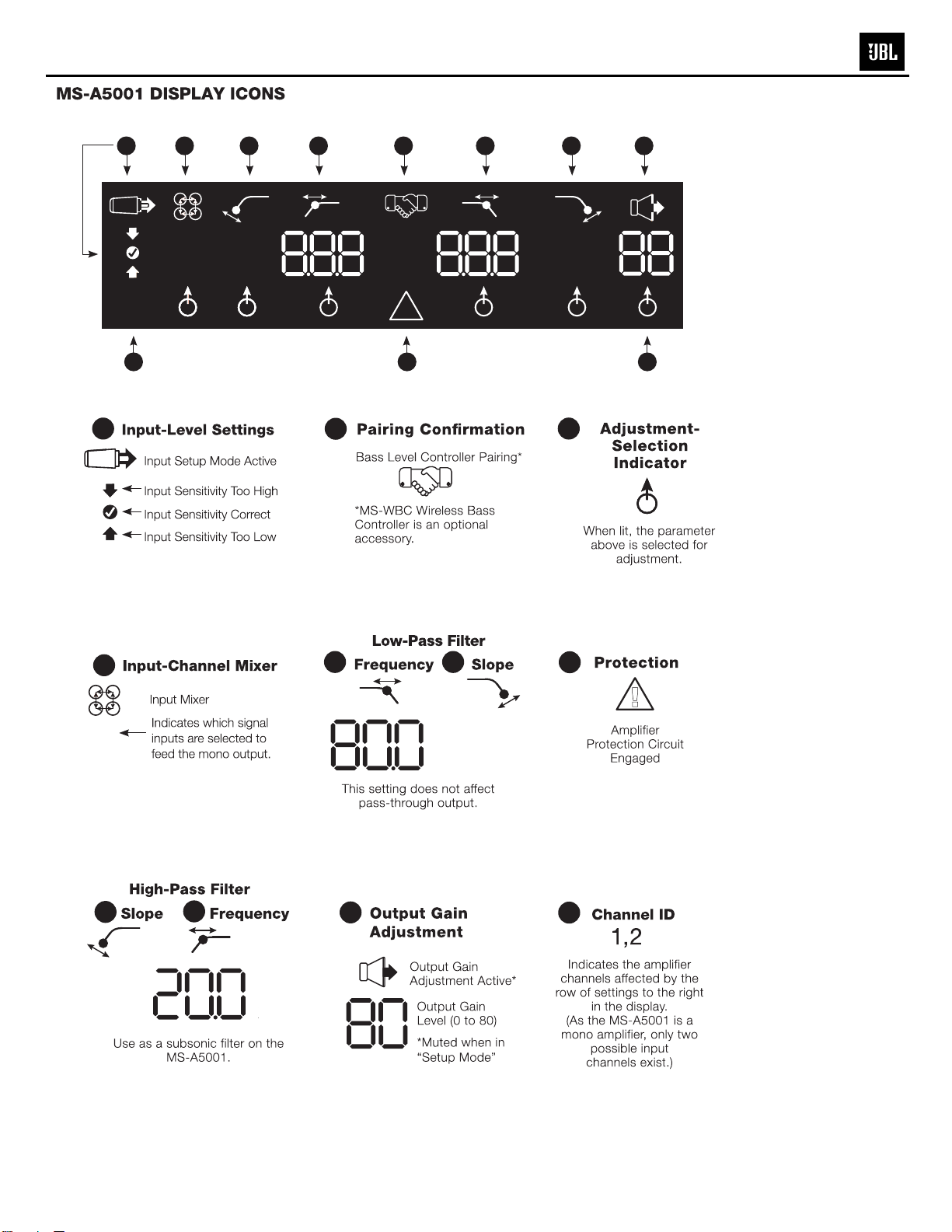
9
MS-A5001
1
1,2
11 10
1
2
1,2
3
1
6dB
12dB
24dB
4 5
5
kHz
!
6
kHz
7
6dB
12dB
24dB
8
9
9
2
1
1,2
3
6dB
12dB
24dB
6 7
10
!
6dB
12dB
kHz
4
8
kHz
24dB
11
Page 11
10
MS-A5001
Page 12
11
MS-A5001
Page 13

Main Amp
12
MS-A5001
MS-A1004 / MS-A5001 CAR AMPLIFIER BLOCK DIAGRAM
BATT+
REM
GND
Head Unit
VCAR
Power Supply
REM_IN_ACT
VCC
VCAR
Auto
Sense
OFF
ON
VEE
VBIAS
GND
Power Regulator
(TDA3681)
User Interface Display
VCAR
HEVN
5V
PWREN
DC 12V
GND
Flexible
5V_ON
3P3V_ON
3V
u-Control
PWREN
OCP, OTP
2.4GHz
Wireless
Receive
VEE
VBIAS
WBC
Tramsmit
3.0V Coin Battery
VCC
(Wireless Bass Control)
Input Select
VDIF,+8P5VA,
Lo
Hi1(x10)
Hi2
-8P5VA
Line-Out
I2S
3P3V-ON
(STA-309)
DSP
(AK4382)
I2S
5V-ON 5V-ON
ADC
(AK5384)
DAC
Class-D
(IR6645)
Page 14
13
MS-A5001
Page 15
14
MS-A5001
Page 16
15
MS-A5001
Page 17
16
MS-A5001
Page 18
17
MS-A5001
Page 19
18
MS-A5001
Page 20
19
MS-A5001
Page 21
20
MS-A5001
Page 22
21
MS-A5001
Page 23
22
MS-A5001
Page 24
23
MS-A5001
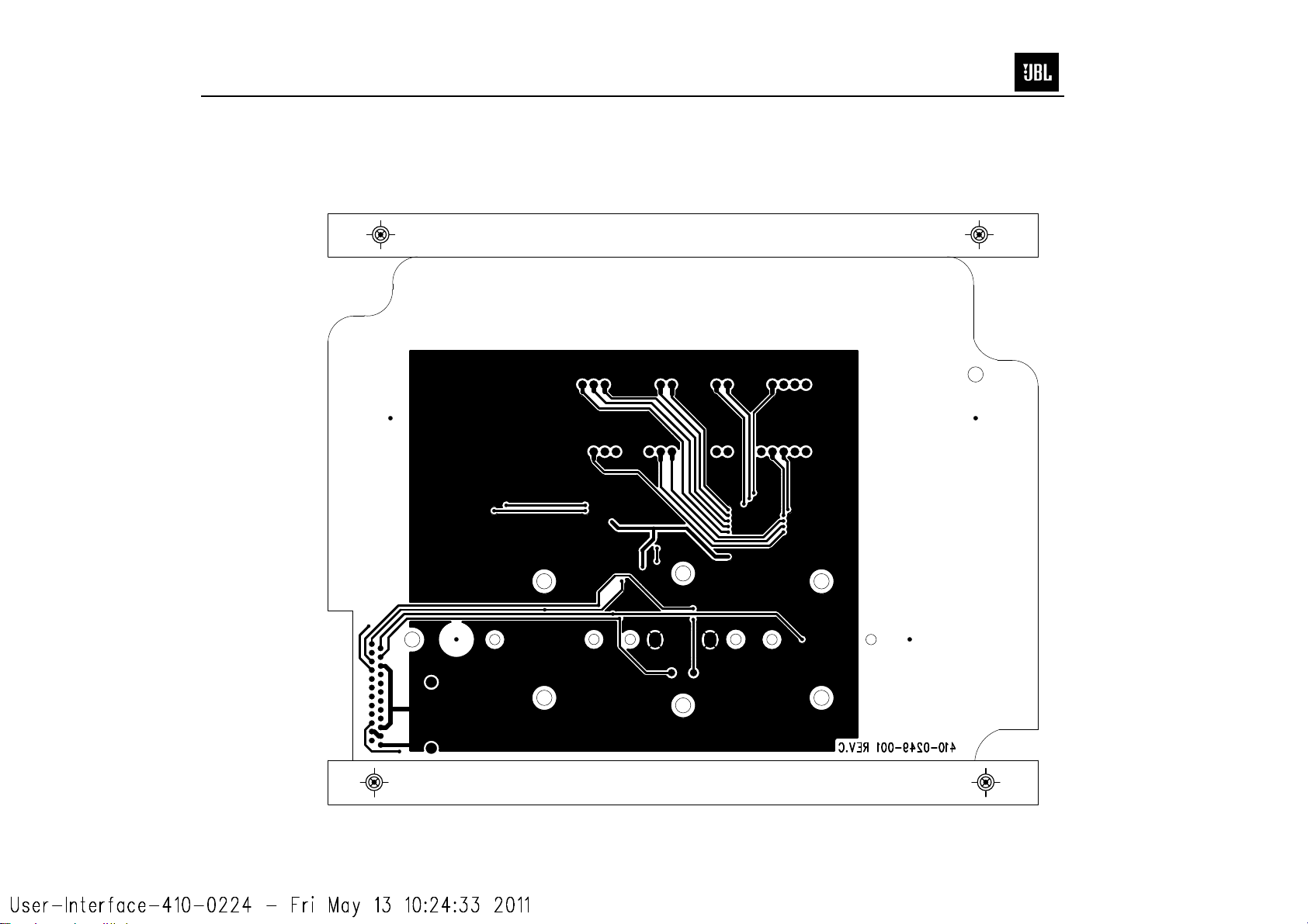
MS-A5001 Electrical Parts List
Part Number Qty
Description
PREAMP/INPUT PCB
Semiconductors
IC-74AHC1G04 SMD IC 74AHC1G04 TSS0P5 INVERTER 1 U24
IC-TL074ID SMD IC TS974,TL074ID QUAD OP-AMP 1 U4
FET-FDV3O1N SMD IC MOSFET_N-CHAN,FDV301N 2 Q8,25
IC-TPS77033 SMD IC TPS7101Q_1,TPS77033 LINEAR REGULATORS 1 VR4
IC-LM224 SMD IC TS974,LM224 so-14 QUAD OP-AMP 2 U10,11
IC-ADTL082ARZ SMD IC TLC082,ADTL082ARZ DUAL OP-AMP 1 U15
IC-TL072ID SMD IC TL072,TL072ID DUAL OP-AMP 1 U5
IC-IRS20957S SMD IC
IC-AK4382VTP SMD IC
IC-AK5384VTP SMD IC
IC-nRF24L01+ SMD IC nRF24l01+QFN-24 RF-transceiver 1 U23
IC-STA309A SMD IC STA309A Multi-channel digital audio processor 1 U17
IC-MC9S08GT16 SMD IC
DIODE-BAV99 SMD diode BAV99_SOT23,BAV99 5 D9,18,19,21,24
DIODE-LL4148WS SMD diode 1N4148,1N4148WS SOD-523 5 D2,10,12,15,20
DIODE-LL4148WT SMD diode 1N4148,1N4148WT SOD-323 9 D27,28,31,34,35,36,40,41,46,
DIODE-ZMM20 SMD zener diode ZENER, 20V/0.5W,MINI MELFZMM20 1 D1
DIODE-MMSZ4689 SMD diode MMSZ4689 1 D5
DIODE-ZMM9R1 SMD zener diode ZENER, 10V/1W,SOD-106PTZ9.1B 1 D3
TR-BT3906 SMD transistor MMBT3906/SOT_233,MMBT3906 5 Q1,7,11,13,14
TR-BT3904LT1 SMD transistor MMBT3904/SOT_23,MMBT3904 4 Q2,6,27,34
FET-IRF6645TRBF SMD transistor MOSFET_IRF6645,IRF6645TRPBF 8 Q17,18,19,20,21,22,23,24
TR-YKTA1661 SMD transistor SMALL SIGNAL PNP,SOT-89KTA1661Y 1 Q3
IC-TL072ID SMD IC TL072,TL072ID SINGLE OP-AMP 2 U1,2
IC-TDA3681 SMD IC
DIODE-MURA120 SMD diode MURA120 4 D37,38,39,42
DIODE-BAV99 SMD diode BAV99,BAV99/SOT 2 D33,45
DIODE-LL4148WS SMD diode 1N4148,1N4148WS SOD-523 1 D13
IRS20957STRPBF SO-16 HIGH/LOW SIDE DRIVER
AK4382VTP (TSSOP-16)DAC, 24-bit 112dB stereo
AK5384VTP (TSSOP-16)ADC, 24-bit 107dB 4-chan
MC9S08GT8ACFBE, (QFP44) 8 BIT 32K FLASH 4K RAM
TDA3681(SOT418-3),MULTIPLE VOLTAGE REGULATOR
2 U18,19
1U9
1U6
1 U22
1 VR2
Reference Designator or Application
Resistors
RES-1002-0805-F SMD Resistor CR0805RESISTORA,10k,1% 2 R195,201
RES-10R0-0805-F SMD Resistor CR0805RESISTORA,10 ohm,1% 2 R212,214
RES-1R00-0805-F SMD Resistor CR0805RESISTORA,1 ohm,1% 2 R219,222
RES-3002-0805-F SMD Resistor CR0805RESISTORA,30k,1% 2 R180,182
RES-4120-0805-F SMD Resistor CR0805RESISTORA,412,1% 2 R133,153
RES-5101-0805-F SMD Resistor CR0805RESISTORA,5.1k,1% 4 R186,192,203,204
RES-1001-0603-F SMD Resistor CR0603RA, 1k,1% 11 R44,46,52,54,,147,149,190,191,193,194,263
RES-1002-0603-F SMD Resistor CR0603RA, 10k 1% 13 R26,32,37,50,55,56,62,85,142,255,271,280, 281
RES-1003-0603-F SMD Resistor CR0603RA, 100k,1% 8 R4,75,111,124,130,138,167,369
RES-100-0603-F SMD Resistor CR0603RB, 10,1% 10 R2,67,76,250,252,253,264,273,277,311
RES-1101-0603-F SMD Resistor CR0603RE, 1.1k,1% 2 R154,267
RES-1203-0603-F SMD Resistor CR0603RA, 120k,1% 2 R90,112
RES-000-0603-F SMD Resistor CR0603RA, 0ohm ,1% 4 R19,20,23,24
RES-1502-0603-F SMD Resistor CR0603RE, 15k,1% 1 R283
RES-2002-0603-F SMD Resistor CR0603RA, 20k,1% 3 R121,125,237
RES-1003-0603-F SMD Resistor RES SMD 100KF 1/10W 0603 3 R3,110,131
RES-2201-0603-F SMD Resistor CR0603RE, 2.2k,1% 4 R35,41,64,72
RES-2202-0603-F SMD Resistor CR0603RE , 22k,1% 2 R144,266
RES-2263-0603-F SMD Resistor CR0603RA, 226k,1% 2 R107,115
RES-2804-0603-F SMD Resistor CR0603RA, 2.8M,1% 1 R78
RES-3003-0603-F SMD Resistor CR0603RA, 300k,1% 2 R74,320
RES-3301-0603-F SMD Resistor CR0603RA, 3.3k,1% 2 R140,168
RES-3321-0603-F SMD Resistor CR0603RE, 3.32k,1% 2 R211,213
RES-33R0-0603-F SMD Resistor CR0603RB, 33ohm,1% 4 R256,276,289,361
RES-2200-0603-F SMD Resistor CR0603RB, 220ohm,1% 2 VA2,3
RES-3300-0603-F SMD Resistor CR0603RB, 330F 1% 4 R357,358,359,360
RES-3902-0603-F SMD Resistor CR0603RA, 39k,1% 2 R82,99
RES-4022-0603-F SMD Resistor CR0603RA, 40.2k,1% 2 R134,135
RES-4023-0603-F SMD Resistor CR0603RA, 402k,1% 1 R84
RES-4301-0603-F SMD Resistor CR0603RA, 4.3k,1% 3 R34,65,261
RES-4700-0603-F SMD Resistor CR0603RB, 470,1% 3 R160,162,236
Page 25
24
MS-A5001
Part Number Qty
Description
PREAMP/INPUT PCB
RES-4701-0603-F SMD Resistor CR0603RA, 4.7k,1% 13 R5,6,11,13,42,66,86,91,143,150,159,161,268
RES-4532-0603-F SMD Resistor CR0603RA, 45.3k,1% 4 R17,18 ,21,22,
RES-4751-0603-F SMD Resistor CR0603RA, 4.75k,1% 2 R217,220
RES-4753-0603-F SMD Resistor CR0603RA, 475k,1% 6 R73,83,102,106,108,114
RES-47R0-0603-F SMD Resistor CR0603RE, 47,1% 2 R179,181
RES-4871-0603-F SMD Resistor CR0603RA, 4.87k,1% 1 R103
RES-5621-0603-F SMD Resistor CR0603RE, 5.62k,1% 2 R218,221
RES-6201-0603-F SMD Resistor CR0603RA, 6.2k,1% 2 R258,282
RES-6202-0603-F SMD Resistor CR0603RA, 62k,1% 2 R96,118
RES-7871-0603-F SMD Resistor CR0603RA, 7.87k,1% 3 R123 ,207,208
RES-8450-0603-F SMD Resistor CR0603RA, 845,1% 1 R109
RES-2700-2512-F SMD Resistor RES SMD 270F 1W 2512 1 R352
RES-4990-2512-F SMD Resistor MOR,1WJ 499 OHM 1 R1
RES-2002-1206-F SMD Resistor CR1206RESISTORA,20k,1% 2 R174,175
RES-5R0-3W-F SMD Resistor CR2512RESISTORA,5ohm 3w,1% 2 R241,242
RES-1004-0402-F SMD Resistor CR0402RA, 1.00M,1% 1 R239
RES-000-0402-F SMD Resistor CR0402RA, 0ohm,1% 1 C21
RES-2202-0402-F SMD Resistor CR0402RA, 22.0k 1% 1 R240
RES-000-0603-F SMD Resistor RES SMD 0R0 1/10W 0603 1 L10
RES-4872-0603-F SMD Resistor CR0603RESISTORA,48.7k,1% 1 R173
RES-10R0-0805-F SMD Resistor CR0805RESISTORA,10 ohm,1% 4 R284,290,291,292
RES-2002-0603-F SMD Resistor CR0603RB, 20K,1% 1 R288
RES-100-0603-F SMD Resistor CR0603RB, 10,1% 2 R274,279
RES-1001-0603-F SMD Resistor CR0603RB, 1k,1% 2 R342,345
RES-1131-0603-F SMD Resistor CR0603RB, 1.13k,1% 2 R341,344
RES-1002-0603-F SMD Resistor CR0603RB, 10k,1% 2 R278,287
RES-3601-0603-F SMD Resistor
RES-4701-0603-F SMD Resistor CR0603RA, 4.7k,1% 4 R332,333,334,335
RES-1003-0603-F SMD Resistor CR0603RE, 100k,1% 4 R295,296,297,303
RES-1003-0603-F SMD Resistor RES SMD 100KF 1/10W 0603 1 R362
RES-5111-0603-F SMD Resistor RES SMD 5.11KF 1/10W 0603 1 R235
RES-3003-0603-F SMD Resistor CR0603RE, 300k,1% 2 R245,246
RES-3401-0603-F SMD Resistor CR0603RE, 3.40k,1% 1 R269
RES-7502-0603-F SMD Resistor CR0603RE, 75k,1% 2 R298,304
RES-9531-0603-F SMD Resistor CR0603RE, 9.53k,1% 1 R178
RES-2200-0603-F SMD Resistor CR0603RB, 220ohm,1% 1 VA1
RES-1R00-1210 SMD Resistor RESISTORA,1 ohm 1210 1/3 W,1% 2 R231,232
RES-ESDA-0603 SMD static Resistor 0603ESDASURGX,0603ESDA 4 SX3,4,9,10
RES,SMD 3.6KF 1/10W 0603
2 R25,47
Reference Designator or Application
Capacitors
CAP0501R0-0402 SMD Capacitor CC0402CD, 1.0pF/50V,+/-0.1pF 1 C161
CAP0501R5-0402 SMD Capacitor CC0402CD, 1.5pF/50V,+/-0.1pF 1 C159
CAP0164R7-0402 SMD Capacitor CC0402CD, 4.7pF,+/-0.25pF 1 C158
CAP050222-0402 SMD Capacitor CC0402CD, 2200pF,10% 1 C157
CAP050270-0402 SMD Capacitor CC0402CD, 27pF,2% 2 C152,160
CAP050102-0603 SMD Capacitor CC0603CA, 1000pF,10% 7 C52,80,81,106,107,154,220
CAP050470-0603 SMD Capacitor CC0603CB, 47pF,10% 14 C7,11,15,16,30,33,44,49,79,85,92,114,129, 131
CAP016333-0402 SMD Capacitor CC0402CD, 0.033uF,16V10% 1 C153
CAP050103-0603 SMD Capacitor CC0603CD, 0.01uF,10% 1 C155
CAP050104-0603 SMD Capacitor CC0603CE, 0.1uF,10% 27
CAP050105-1206 SMD Capacitor CC1206CE, 1uF cer,10% 6 C40,41,171,176,192,201
CAP050224-1206 SMD Capacitor CC1206CB, 0.22uF/1206,5% 10 C8,14,19,29,37,42,94,185,190,198
CAP050225-0805 SMD Capacitor CC0805CA, 2.2uF cer,10% 9 C13,34,35,65,73,74,76,141,142
CAP050472-0603 SMD Capacitor CC0603CE, 4700pF,10% 2 C90,102
CAP050152-0603 SMD Capacitor CC0603CE, 1500pF,10% 2 C265,266
CAP025106-1206 SMD Capacitor CC1206CA, 10uF cer,-20%_+80% 11 C57,61,77,91,130,132,137,138,146,178,187
CAP050102-0805 SMD Capacitor SMD"0805"50V10%102 Pf 4 C274,275,276,277
CAP0316100-4 SMD EL Capacitor SMTCAN_SIZE-BC_ELECTB,10uF/16V,20% 11 C5,9,10,17,24,25,31,53,248,258,259
CAP0316221-6.3 SMD EL Capacitor 220UF/16V 6.3 20% 1 C1
CAP1025100-B SMD Ta EL Capacitor 10uf/25V “B” type 1 C39
CAP10251R0-A SMD Ta EL Capacitor 1uf/25v “A” type 1 C56
CAP1016101-D SMD Ta EL Capacitor 100uf/16V “D” type 2 C38,72
CAP1016100-A SMD Ta EL Capacitor 10uf/16V “A” type 1 C55
CAP0316220-4 SMD EL Capacitor SMTCAN_SIZE-BC_ELECTB,22uF/16V,20% 1 C110
CAP0335100-5 SMD EL Capacitor SMTCAN_SIZE-BC_ELECTB,10uF/35V,20% 2 C88,101
C6,12,46,47,66,70,120,121,125,126,180,182,183,188,193,19
6,197,206,207,210,214,233, 262,270,271,272,273
Page 26
25
MS-A5001
Part Number Qty
Description
PREAMP/INPUT PCB
Reference Designator or Application
CAP036R3330-6.3 SMD EL Capacitor
CAP0335330-5 SMD EL Capacitor
CAP0350221-8 SMD EL Capacitor
CAP0616330-5 SMD NP EL Capacitor CAPACITOR_NON-POL,33uF 16V Bipolar,20% 3 C89,103,162
CAP050221-0603 SMD Capacitor CC0603CA, 220pF,10% 1 C99
CAP050470-0603 SMD Capacitor CAP, SM 47PF 50V 5%NPO 0603 2 C184,189
CAP050102-0603 SMD Capacitor CAP, SM 102PF 50V 5%NPO 0603 4 C50,51,54,58
CAP050104-0603 SMD Capacitor CC1210CA, 0.1uF 100v,10% 7 C2,3,69,172,230,231,232
CAP050104-0805 SMD Capacitor CAP, SM 0.1UF 100V 10%NPO 0805 8 C147,148,224,225,226,227,228,229
CAP050104-0603 SMD Capacitor CC0603CE, 0.1uF,10% 11 C200,203,204,205,208,209,211,213,215,216,217
CAP050105-1206 SMD Capacitor CC1206CE, 1uF cer,10% 1 C212
CAP050122-0603 SMD Capacitor CC0603CE, 1200pF,10% 1 C194
CAP025106-1206 SMD Capacitor CAP, SM 10UF cer -20%+80% 25V 1206 5 C36,45,59,60,98
CAP050225-0805 SMD Capacitor CC0805CA, 2.2uF cer,10% 1 C199
CAP250104-M cassette Capacitor 0.1uf 250V CBB21B 2 C164,166
CAP250474-M cassette Capacitor 0.47uf 250V CBB21B 2 C163,165
Miscellaneous
CORE-1R0-0603 SMD Inductor 1nH 0603 +/-0.1nH 3 L3 L12 ,L13
CORE-2R7-0402 SMD Inductor 2.7nH 0402 +/-0.1nH 1 L5
CORE-3R9-0402 SMD Inductor 3.9nH 0402 +/-0.1nH 1 L7
CORE-8R2-0402 SMD Inductor CL0402INDUCTOR,8.2nH,5% 1 L6
CORE-220M Inductor 22UH 7G17B-220M 2 L8,9
CNCTR-24-1R0 24P neilsbed CNCTR, FPC/FFC 24P 1MM VER PCB horizontal 1 J3
RET- 120-F thermistor PTC,Vishay 2381 660 56393 2 RT3,4
CY-SMT-12.288M SMD crystal oscillator
CY-SMT-16M SMD crystal oscillator CRYSTAL_0,16MHz 15pF 1 Y2
CORE-DS80-0603 SMD magnetic ring CL0603FERRITE_BEAD,600ohm @ 100mhz 2 FB1,2
W-5-100MM 5P harness neilsbed using harness of 26AWG 100MM 1 J8
RET- 50K-105 thermistor+wire FTD5-350 50K length:105 1 RT9
CNCTR-06-2R0 6P neilsbed CON6A 6P 2*3P 1 J2
5-C50K-90 potentiometer
RCA JACK*4 RCA connector RCA JACK*4 1 J5
3PSK-43D01K switch
CONRA-07-200 7P neilsbed CONRA-07-200 1 CON6
SMTCAN_SIZE-BC_ELECTB,33UF/6.3V,¢5 20%
SMTCAN_SIZE-BC_ELECTB,33UF/35V,¢5 20%
EMZA500ADA221MJA0GC_ELECTB,220uF/50V,20%
(12.288MHz ) OSC 12.288MHZ /15PF 50PPM 3.3V SMD 7050
ALPS_RK09L12B0A31POT_DUAL,50k DUAL POT LEVEL
SK43D03SW_4P3T_(EG4319),SW 4P3T (EG4319) LO-HI-HI2
1 C32
1C4
4 C124,144,151,156
1 OSC1
1 RV2
1 SW3
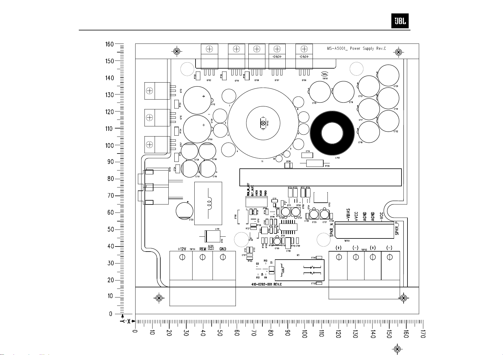
POWER PCB
Semiconductors
IC-TL494 SMD IC PWM IC,SO-16TL494CD 1 U701
IC-KIA7812 SMD IC KIA7812 POSITIVE 12V REGULATOR 1 U702
DIODE-ZMM15 SMD diode ZENER, 15V/500mW,MINI MELFZMM15 1 D703
DIODE-LL4148WT SMD diode 1N4148WT,1N4148WT 2 D704 D705
DIODE-LL4937 SMD diode 1N4148WT,LL4937 1 D709
DIODE-SMCJ24A SMD diode
DIODE-LL4004 SMD diode RECTIFIER,1A, LL4004G 1 D1
TR-KDS184 SMD diode EPITAXIAL PLANAR NPN "SOT-23",KDS184 1 D702
TR-GRKRC102 SMD transistor KRC102S SOT-23 1 Q706
TR-BT3904LT1 SMD transistor MMBT3904 SOT-23 3 Q4,5,701
TR-BT3906 SMD transistor MMBT3906/SOT_233,MMBT3906 2 Q708,711
TR-YKTA1661 SMD transistor SMALL SIGNAL PNP "SOT-89",KTA1661Y 1 Q703
TR-FRF1620D diode FAST RECOVERY FRF1620D 2 D706, D707
TR-A60 diode RECTIFIER6A06 1 D701
FET-IRF3205 MOSFET MOSFET_IRFB4227,IRF3205 6 Q702 Q707 Q709 Q710 Q712 Q713
Resistors
RES-4701-0603-F SMD Resistor CR0603RA, 4.7k 1% 1 R10
RES-1002-0603-F SMD Resistor CR0603RA, 10k 1% 2 R9,12
RES-000-0805-F SMD Resistor SMD-0805 RESISTOR,0F 1 R703
RES-10R0-0805-F SMD Resistor SMD-0805 RESISTOR,10F 1 R707
RES-1002-0805-F SMD Resistor SMD-0805 RESISTOR,10KF 1 R727
RES-1502-0805-F SMD Resistor SMD-0805 RESISTOR,15KF 2
RES-1001-0805-F SMD Resistor SMD-0805 RESISTOR,1KF 2 R729 R730
RES-2202-0805-F SMD Resistor SMD-0805 RESISTOR,22KF 3 R709 R711 R712
ZD,SMC J24A DO-214AB
1 D708
R705,R710
Page 27

26
MS-A5001
Part Number Qty
Description
POWER PCB
RES-3302-0805-F SMD Resistor SMD"0805" 1/8W 33KF 1 R713
RES-2004-0805-F SMD Resistor SMD-0805 RESISTOR,2MF 1 R708
RES-4701-0805-F SMD Resistor SMD-0805 RESISTOR,4.7KF 2 R702 R728
RES-4702-0805-F SMD Resistor SMD-0805 RESISTOR,47KF 2 R714 R715
RES-6800-0805-F SMD Resistor SMD-0805 RESISTOR,680F 1 R706
RES-101-1206-J SMD Resistor SMD-1206 RESISTOR,100J 6 R718 R719 R720 721 R724 R725
RES-471-1206-J SMD Resistor SMD-1206 RESISTOR,470J 2 R716 R722
RES-102-1206-J SMD Resistor SMD-1206 RESISTOR,1KJ 2 R717 R723
RES-3301-0805-F SMD Resistor SMD-0805 RESISTOR,3.3KF 1 R731
RES-ESDA-0603 SMD static Resistor SURGX,0603ESDA 1 SX701
RES101-2W Resistor MOR,2WJ 100 OHM 1 R726
Capacitors
CAP050105-0805 SMD Capacitor CAPACITOR,105P 2 C707,C735
CAP050102-0805 SMD Capacitor CAPACITOR,1NF 2 C733 C734
CAP050104-0805 SMD Capacitor CAPACITOR,100NF 7 C702 C709 C711 C721 C722 C726 C728
CAP050104-1206 SMD Capacitor 0.1UF 104 50V ±5% 1206 1 C724
CAP0316100-4 SMD EL Capacitor ELECTROLYTIC"MVG" 5%, 4 10/16V 1 C705
CAP0316101-6.3 SMD EL Capacitor ELECTROLYTIC"MVG" 5%, 6.3 100/16V 1 C701
CAP0316470-5 SMD EL Capacitor ELECTROLYTIC"MVG" 5%,5 47/16V 3 C708 C725 C727
CAP100102-M cassette Capacitor BOX 100V 5%102J 1 C706
CAP400222-M cassette Capacitor BOX 400V 5%222K 1 C714
CAP025471-E electrolytic Capacitor EC,470uF/25V 5 C710,C723, C729,C730,C731
CAP050102-E electrolytic Capacitor 1000/50V SHL/MHC 16*20 4 C715,716,718,720
CAP050681-E electrolytic Capacitor 680/50V MHC/WL 13*20 4 C713,717,719,732
CAP025182-E electrolytic Capacitor EC,1800uF/25V(20*16) 2 C703 C712
Reference Designator or Application
Miscellaneous
W-7-90MM 7P harness harness16AWG 90MM 1 TB703
CORECL-1700B Inductor IRON CORECL-1700B 1 L702
CONRA-07-200 7P neilsbed CONRA-07-200 1 TB703
20PWF-08031 fuse socket FUSERA,BXS2-09 2 FH701
24.11.004023 fuse 40A LITE 2 FH1
CORECL-310A Inductor CL-310 1 L701
CNCTR-5-2R5 5P neilsbed 5P pin P=2.5mm 1 CON5
RET- 50K-F thermistor FTD5-350 50K 1 TH701
RET- 49K-F thermistor DIODE TYPE, 49KOHM +/-3%KCD493H399G 1 TH702
CORE-MSA5001 transformer ZF43813 5T(1.2x5):14T(1.5x1) +8T(1.0x1) 1 T1
TER-JSZ4-80 4P connector JSZ4-80 1 TB702
TER-JSZ3-79 3Pconnector JSZ3-79 1 TB701
SCR-M3*6 MI screw BMB PH M3*6 MI-P 4 P1 P2 2PCS
AA-PPRC0 relay SWITCH, RELAY DPST 5A 12V 1 K1
FIBER7-200 paper pad 200MM*7 *0.4 0.3 Q707,712,713
FIBER6-200 paper pad 200MM*6 *0.3 0.4 Q702,709,710,D706,707
DISPLAY PCB
Semiconductors
IC-74HCT SMD IC 74HCT238/SO SO16 3-to-8 decode-demultiplxr 1 U502
IC-MIC2982YWM SMD IC MIC2982YWM SSOP-20 Driver Array 1 U503
IC-A6276ELW SMD IC
TR-FTZ506E SMD diode FTZ506E 1 DP501
IC-BA50D SMD IC BA50DD0WHFP HRP5 REGULATOR 1 Q1
LED-LTG-0732M LED
A6276ELW SSOP-20(24)16-BIT SERIAL-INPUT LED DRIVER
MTINYAMP_LED_DISPLAY,LTG-0732M LED Display
1 U501
1 LED501
Resistors
RES-2700-0805-F SMD Resistor RES SMD 270F 1/8W 0805 1 R501
RES-4302-0603-F SMD Resistor CR0603RB, 43KF,1% 4 R503 R504 R507 R508
RES-6202-0603-F SMD Resistor CR0603RB, 62KF,1% 4 R502 R505 R511 R512
RES220-2W carbon film Resistor
RES,CF 22R OHM 2W ±5%
1R3
Page 28

27
MS-A5001
Part Number Qty
Description
DISPLAY PCB
Capacitors
CAP050104-0603 SMD Capacitor CAP, SM 104PF 50V 10% 0603 2 C502 C503
CAP050104-0805 SMD Capacitor SMD"0805" 50V 10% 104P 2 C1,3
CAP0310102-10 SMD EL Capacitor
CAP0325220-4 SMD EL Capacitor ELECTROLYTIC"CHIP""SC/MV"5PHI22uF/25V 1 C2
Miscellaneous
ELECTROLYTIC"MVG/SC" 20%, 10Φ1000uF/10V 1C6
Reference Designator or Application
20F7-12C12P encoder
29.142.04R30 switch 0.5A handle length is 1MM 2 SW501 SW502
CNCTR-24-1R0 24P neilsbed CNCTR, FPC/FFC 24P 1MM VER PCB horizontal 1 J501
32.13.0563R005271 screw STT2 BH, 3x5 NI washer 1
31.11.0513R00610 screw SMB M3x6 NI-P 3
HEA-AL 6063 heatsink
ALP5 ENCODER (EC12E1220406)EC1201H-20F7-12C12
(AL 6063,16.0mm×101mm×23mm)
1 ENC501
1
MECHANICAL/MISCELLANEOUS
41.1.TINY1R50070 upper cover AL/ADC12 1 Silver Paint
42.1.TINY1R50070 bottom cover AL/ADC12 1 Black Sanding Paint/silk
35.1.TINY4R10030 power supply knob Silver Plated ABS 1 Silver Plated
35.1.TINY4R100300 volume button Silver Plated ABS 2 Silver Plated
50.12.TINY4R10010 knob bracket ABS 1 Polishing
43.11.TINY4R1000 acryl Acryl GRAY 1
50.13.TINY4R10010 copper column BSBM 5.0 4
53.14.045001500371 heatsink SPCC3.0,L=45mm 1
53.14.069001500371 heatsink SPCC3.0,L=69mm 1
48.171.0180090020 nowoven cloth FELT 18.0x9.0x2t 1
48.142.035023R201 silicone film 35mm 23mm 0.2mm 1 USED ON HEATSINK
48.142.070018R202 silicone film HF300P,70mm×18mm×0.2mm 1
48.142.045020R202 silicone film HF300P,45mm×20mm×0.2mm 1
32.13.0563R005271 screw STT2 BH, 3x5 NI washer 1
33.14.0200200061 plasticene 20X20X6 GAP PAD 1500 1 7812 underside
24.11.004023 fuse 40A LITE 2 FH1
48.152.0320320R50 paper pad 32mm 32mm 0.5mm 1 C18,20,21
48.152.1541130R50 paper pad single glued 1 shield cover
48.152.1541130R52 paper pad flexible paper 0.5T,single glued 1 shield cover
50.12.SW30012 spacer 1 between screw and heatsink
31.11.0213R01400 screw SMP 3x14 BK 1 fix small heatsink
18.1240.0006050 24P harness soft harness 24P 60MM 1 J3-LED PCB J501
31.11.0913R00610 screw DF SERIES , M3x6 NI-P 4 DF SERIES USED ON LED PCB AND TOP COVER
31.13.0963R00610 screw DF SERIES , M3x6 NI-P 6 DF SERIES USED ON LED PCB AND KNOB
31.11.0513R00610 screw SMB M3x6 NI-P 10
31.13.0563R01000 screw STT2 BH, 3x10 BLACK 2 RCA JACK
31.11.0514R02000 screw SMB M4*20 BLACK 4
31.11.0564R01411 screw SMB M4x14 NI-P LOCK HEAD 4
31.11.0413R01210 screw SCREW, M3X12 90CS FLAT PHIL 2
53.12.0210016R100
34.19.0030030054 AL column H5 L=3 diameter of the hole is 3 2
54.11.1080 bunch 80mm 2
63.15.TINY4R10010 shield cover Tinplate 0.2T 1
piezo ceramic heatsink 21*16*0.1t(MM) 1 for VR2
Page 29

28
MS-A5001
Philips Semiconductors Product specification
Multiple voltage regulator with switch and
ignition buffer
FEATURES
General
• Extremely low noise behaviour and good stability with
very small output capacitors
• Second supply pin for regulators 3 and 4 to reduce
power dissipation (e.g. via a DC-to-DC converter)
• Three VP-state controlled regulators (regulators 1, 3
and 4) and a power switch
• Regulator 2, resetand ignitionbuffer operationalduring
load dump and thermal shutdown
• Combined control pin for switching regulators 1 and 3
• Separate control pins for switching regulator 4 and the
power switch
• Supply voltage range from −18 to +50 V
• Low quiescent current in standby mode (when
regulators 1, 3 and 4 andpower switchare switchedoff
and ignition input is low)
• Hold outputfor low VP(regulators 1, 3 and 4 andpower
switch off)
• Hold output when one of regulators 1 and 3 and/or 4 is
out of regulation
• Hold output for foldback mode of power switch and
regulators 1, 3 and 4
• Hold output for load dump and temperature protection
• Reset (push-pull output stage) for regulator 2 and hold
output (open-collector output)
• Adjustable reset delay time
• High supply voltage ripple rejection
• Backup capacitor for regulator 2
• One independent ignition buffer (active HIGH).
Protections
• Reverse polarity safe (down to −18 V without high
reverse current)
• Able to withstand voltages up to 18 V at the outputs
(supply line may be short-circuited)
• ESD protection on all pins
• Thermal protections
• Load dump protection
• Foldback current limit protection for regulators 1, 2, 3
• Delayed second current limit protection for the power
• The regulator outputs and the power switch are
GENERAL DESCRIPTION
The TDA3681is a multiple output voltageregulator with a
power switch andanignition buffer. Itis intended foruse in
car radioswith orwithout amicrocontroller. The TDA3681
contains the following:
• Four fixed voltage regulators with a foldback current
• Regulators 3 and 4 have a second supply pin that can
• A power switch with protection, operated by a control
• Reset and hold outputs that can be used to interface
• Both supply pins can withstand load dump pulses and
• Regulator 2, which is in regulation at a backup voltage
• A provisionforthe use ofa reserve supplycapacitorthat
• An ignition input Schmitt trigger with push-pull output
TDA3681
and 4
switch (at short-circuit)
DC short-circuit safe to ground and supply (VP).
protection (regulators 1, 2, 3 and 4). Regulator2, which
is intended to supply a microcontroller, also operates
during load dump and thermal shutdown
be connected to a lower supply voltage (>6.5 V) to
reduce the power dissipation
input
with themicrocontroller; the reset signal canbe used to
call up the microcontroller
negative supply voltages
above 6.5 V
will hold enough energy for regulator 2 (5 V continuous)
to allow a microcontroller to prepare for loss of voltage
stage.
ORDERING INFORMATION
TYPE
NUMBER
TDA3681J DBS17P plastic DIL-bent-SIL power package; 17 leads (lead length 7.7 mm) SOT243-3
TDA3681JR DBS17P plastic DIL-bent-SIL (special bent) power package; 17 leads
TDA3681TH HSOP20 plastic, heatsink small outline package; 20 leads; low stand-off height SOT418-2
NAME DESCRIPTION VERSION
(lead length 12mm)
PACKAGE
SOT475-1
Page 30

29
MS-A5001
Philips Semiconductors Product specification
Multiple voltage regulator with switch and
ignition buffer
handbook, full pagewidth
V
P1
ENSW
V
EN4
HEATTAB
n.c.
n.c.
P2
(14.4 V)
14
8
20
6
11
15
18
POWER SWITCH
&
BACKUP SWITCH
BACKUP CONTROL
&
&
TEMPERATURE
LOAD DUMP
PROTECTION
REGULATOR 2
REGULATOR 4
REGULATOR 3
16
13
12
1
19
(14 V/
3 A)
(14 V/
100 mA)
(5 V/
300 mA)
(3.3 V/
1 A)
(5 V/
1400 mA)
TDA3681
SW
BU
REG2
REG4
REG3
EN1/3
C
RES
IGN
TDA3681TH
(8.5 V/
600 mA)
7
&
OR
5
IN
2
IGNITION BUFFER
REGULATOR 1
+
&
10
GND
17
MGU353
REG1
9
4
3
HOLD
RES
IGN
OUT
Fig.2 Block diagram of TDA3681TH.
Page 31

30
MS-A5001
Philips Semiconductors Product specification
Multiple voltage regulator with switch and
ignition buffer
Pin description of TDA3681TH
SYMBOL PIN DESCRIPTION
REG4 1 regulator 4 output
IGN
IN
IGN
OUT
RES 4 reset output (active LOW)
C
RES
EN4 6 enable input for regulator 4
EN1/3 7 enable input for regulators 1 and 3
ENSW 8 enable input for power switch
HOLD 9 hold output (active LOW)
GND 10 ground
HEATTAB 11 heat tab connection; note 1
REG2 12 regulator 2 output
BU 13 backup switch output
V
P1
n.c. 15 not connected
SW 16 power switch output
REG1 17 regulator 1 output
n.c. 18 not connected
REG3 19 regulator 3 output
V
P2
2 ignition input
3 ignition output (active HIGH)
5 reset delay capacitor
14 supply voltage
20 second supply voltage
handbook, halfpage
HEATTAB
Fig.4 Pin configuration for TDA3681TH.
V
P2
REG3
n.c.
REG1
SW
n.c.
V
P1
BU
REG2
20
19
18
17
16
TDA3681TH
15
14
13
12
11
MGU329
TDA3681
1
REG4
2
IGN
IN
3
IGN
OUT
RES
4
C
5
RES
EN4
6
EN1/3
7
ENSW
8
HOLD
9
GND
10
Note
1. The pin is used for final test purposes. In the
application it should be connected directly to ground.
Page 32

31
MS-A5001
MC9S08GT16A/GT8A Features
8-Bit HCS08 Central Processor Unit (CPU)
• 40-MHz HCS08 CPU
• HC08 instruction set with added BGND instruction
• Support for up to 32 interrupt/reset sources
Memory Options
• FLASH read/program/erase down to 1.8 V
• Up to 16K FLASH; up to 2K RAM
Power-Saving Modes
• Three very low power stop modes
• Reduced power wait mode
• Very low power real time interrupt for use in run,
wait, and stop
Clock Source Options
• Clock sources to internal hardware frequency
locked-loop (FLL): internal, external, crystal, or
resonator
• Internal clock with ±0.2% trimming resolution and
±0.5% deviation across voltage or across
temperature
System Protection
• Software selectable pullups on ports when used as
input
• Internal pullup on RESET and IRQ pin to reduce
customer system cost
• Up to 38 general-purpose input/output (I/O) pins,
plus one output-only pin, depending on package
selection
Development Support
• Background debugging system
• Breakpoint capability to allow single breakpoint
setting during in-circuit debugging (plus two more
breakpoints in on-chip debug module)
• On-chip, in-circuit emulation (ICE) debug module
with real-time bus capture. On-chip ICE debug
module containing two comparators andnine trigger
modes. Eight deep FIFO for storing change-of-flow
addresses and event-only data.
• Single-wire background debug interface
Package Options
• 48-pin QFN
• 44-pin QFP
• 42-pin PSDIP
• 32-pin QFN
• Optional watchdog computer operating properly
(COP) reset
• Low-voltage detection with reset or interrupt
• Illegal opcode detection with reset
• Illegal address detection with reset
• FLASH block protect and security
Peripherals
• ATD — 8-channel, 10-bit analog-to-digital
converter
• SCI — Two serial communications interface
modules
• SPI — Serial peripheral interface module
• IIC — Inter-integrated circuit bus module
• Timer —One 3-channel timer PWM module (TPM)
plus one 2-channel TPM
• KBI — 8-pin keyboard interrupt module
Input/Output
• 8 high-current pins (20 mA each)
Page 33

32
MS-A5001
Device Overview
REFH
REFL
SSAD
DDAD
V
V
V
V
RESET
NOTE 4
IRQ
NOTES 2, 3
HCS08 CORE
CPU
HCS08 SYSTEM CONTROL
RESETS AND INTERRUPTS
MODES OF OPERATION
POWER MANAGEMENT
RTI
IRQ LVD
BDC
COP
BKGD
8-BIT KEYBOARD
INTERRUPT (KBI)
10-BIT
ANALOG-TO-DIGITAL
CONVERTER (ATD)
INTER-IC (IIC)
SERIAL COMMUNICATIONS
INTERFACE (SCI2)
8
8
SCL
SDA
RXD2
TXD2
PORT A
PORT B
4
4
4
4
PORT C
PTA7/KBIP7–
PTA4/KBIP4
PTA3/KBIP3–
PTA0/KBIP0
PTB7/ADP7–
PTB4/ADP4
PTB3/ADP3–
PTB0/ADP0
PTC7
PTC6
PTC5
PTC4
PTC3/SCL
PTC2/SDA
PTC1/RxD2
PTC0/TxD2
NOTE 6
NOTE 5
USER FLASH
(GT16A = 16,384 BYTES)
(GT8A = 8192 BYTES)
USER RAM
(GT16A = 2048 BYTES)
(GT8A = 1024 BYTES)
ON-CHIP ICE
DEBUG
MODULE (DBG)
INTERNAL CLOCK
GENERATOR (ICG)
LOW-POWER OSCILLATOR
V
DD
V
SS
V
SS
VOLTAGE
REGULATOR
2-CHANNEL TIMER/PWM
(TPM2)
3-CHANNEL TIMER/PWM
(TPM1)
SERIAL PERIPHERAL
INTERFACE (SPI)
SERIAL COMMUNICATIONS
INTERFACE (SCI1)
EXTAL
XTAL
BKGD
= Pins not available in 44-, 42-, or 32-pin packages
= Pins not available in 42- or 32-pin packages
= Pins not available in 32-pin packages
CH1
CH0
CH0
CH1
CH2
SPSCK
MOSI
MISO
SS
RXD1
TXD1
PORT D
PORT E
PORT G
PTD4/TPM2CH1
PTD3/TPM2CLK/TPM2CH0
PTD2/TPM1CH2
PTD1/TPM1CH1
PTD0/TPM1CLK/TPM1CH0
PTE5/SPSCK
PTE4/MOSI
PTE3/MISO
PTE2/SS
PTE1/RxD1
PTE0/TxD1
PTG3
PTG2/EXTAL
PTG1/XTAL
PTG0/BKGD/MS
NOTES:
1. Port pins are software configurable with pullup device if input port.
2. Pin contains pullup/pulldown device if IRQ enabled (IRQPE = 1).
3. IRQ does not have a clamp diode to V
4. Pin contains integrated pullup device.
. IRQ should not be driven above VDD.
DD
5. High current drive
6. Pins PTA[7:4] contain both pullup and pulldown devices. Pulldown available when KBI enabled (KBIPn = 1).
Figure 1-1. MC9S08GT16A/GT8A Block Diagram
Page 34

33
MS-A5001
Device Overview
Table 1-2 lists the functional versions of the on-chip modules.
Table 1-2. Block Versions
Module Version
Analog-to-Digital Converter (ATD) 3
Internal Clock Generator (ICG) 4
Inter-Integrated Circuit (IIC) 1
Keyboard Interrupt (KBI) 1
Serial Communications Interface (SCI) 1
Serial Peripheral Interface (SPI) 3
Timer Pulse-Width Modulator (TPM) 2
Central Processing Unit (CPU) 2
1.2 System Clock Distribution
SYSTEM
CONTROL
ICGERCLK
FFE
ICG
ICGOUT
ICGLCLK*
* ICGLCLK is the alternate BDC clock source for the MC9S08GT16A/GT8A.
LOGIC
RTI
÷2
FIXED FREQ CLOCK (XCLK)
÷2
CPU
BUSCLK
BDC
Figure 1-2. System Clock Distribution Diagram
TPM1 TPM2 IIC SCI1 SCI2 SPI
COP
ATD
ATD has min and max
frequency requirements.
See Chapter 14, “Ana-
log-to-Digital Converter
(S08ATDV3)”
and Appendix A, “Electrical
Characteristics.”
RAM FLASH
FLASH has frequency
requirements for program
and erase operation.
See Appendix A, “Electrical
Characteristics”.
Page 35

34
MS-A5001
Chapter 2
Pins and Connections
2.1 Introduction
This section describes signals that connect to package pins. It includes a pinout diagram, a table of signal
properties, and detailed discussion of signals.
2.2 Device Pin Assignment
DDAD
RESET
PTC0/TxD2
PTC1/RxD2
PTC2/SDA
PTC3/SCL
PTC4
PTC5
PTC6
PTE0/TxD1
PTE1/RxD1
IRQ
11
PTG2/EXTAL
44
1
2
3
4
5
6
7
8
9
10
12
PTG1/XTAL
PTG0/BKGD/MS
43
42
13
14
SSAD
V
41
15
V
40
16
PTA6/KBIP6
PTA7/KBIP7
39
38
17
18
19
PTA4/KBIP4
PTA5/KBIP5
37
36
20
PTA2/KBIP2
PTA3/KBIP3
35
34
33
32
31
30
29
28
27
26
25
24
23
22
21
PTA1/KBIP1
PTA0/KBIP0
V
REFL
V
REFH
PTB7/ADP7
PTB6/ADP6
PTB5/ADP5
PTB4/ADP4
PTB3/ADP3
PTB2/ADP2
PTB1/ADP1
Freescale Semiconductor
SS
SS
PTE2/
PTE3/MISO
PTE4/MOSI
PTE5/SPSCK
DD
V
V
PTB0/ADP0
PTD1/TPM1CH1
PTD0/TPM1CLK/TPM1CH0
PTD4/TPM2CH1
PTD3/TPM2CLK/TPM2CH0
Figure 2-2. MC9S08GT16A/GT8A in 44-Pin QFP Package
MC9S08GT16A/GT8A Data Sheet, Rev. 1
Page 36

35
MS-A5001
2.3 Recommended System Connections
Pins and Connections
Figure 2-5 shows pin connections that are common to almost all MC9S08GT16A application systems. A
more detailed discussion of system connections follows.
SYSTEM
POWER
BACKGROUND HEADER
V
DD
OPTIONAL
MANUAL
RESET
V
+
3 V
C
BLK
10 µF
BKGD/MS
+
ASYNCHRONOUS
INTERRUPT
INPUT
DD
C
BY
0.1 µF
V
DD
4.7 kΩ–10 kΩ
0.1 µF
V
DD
4.7 kΩ–10 kΩ
0.1 µF
C
BYAD
0.1 µF
V
V
V
V
V
V
V
REFH
DDAD
SSAD
REFL
DD
SS
SS
MC9S08GT16A
NOTE4
RESET
NOTE 3
IRQ
NOTE 3
PORT
A
PORT
B
PORT
C
PTA0/KBIP0
PTA1/KBIP1
PTA2/KBIP2
PTA3/KBIP3
PTA4/KBIP4
PTA5/KBIP5
PTA6/KBIP6
PTA7/KBIP7
PTB0/ADP0
PTB1/ADP1
PTB2/ADP2
PTB3/ADP3
PTB4/ADP4
PTB5/ADP5
PTB6/ADP6
PTB7/ADP7
PTC0/TxD2
PTC1/RxD2
PTC2/SDA
PTC3/SCL
PTC4
PTC5
PTC6
PTC7
I/O AND
PERIPHERAL
INTERFACE TO
APPLICATION
SYSTEM
PTG0/BKDG/MS
PTG1/XTAL
PTG2/EXTAL
PTG3
NOTE 1
C1
X1
R
F
C2
R
S
XTAL
EXTAL
NOTES:
1. Not required if using the internal oscillator option.
2. The 48-pin QFN has 2 V
3. RC filters on
RESET and IRQ are recommended for EMC-sensitive applications and systems.
pins (V
SS
Figure 2-5. Basic System Connections
MC9S08GT16A/GT8A Data Sheet, Rev. 1
Freescale Semiconductor
SS1
and V
PORT
G
), both of which must be connected to GND.
SS2
PORT
D
PORT
E
PTD0/TPM1CLK/TPM1CH0
PTD1/TPM1CH1
PTD2/TPM1CH2
PTD3/TPM2CLK/TPM2CH0
PTD4/TPM2CH1
PTE0/TxD1
PTE1/RxD1
SS
PTE2/
PTE3/MISO
PTE4/MOSI
PTE5/SPSCK
Page 37

TPS77001, TPS77012, TPS77015, TPS77018, TPS77025
TPS77027, TPS77028, TPS77030, TPS77033, TPS77050
ULTRA LOW-POWER 50-mA LOW-DROPOUT LINEAR REGULATORS
SLVS210C – JUNE 1999 – REVISED SEPTEMBER 1999
Please be aware that an important notice concerning availability, standard warranty, and use in critical applications of
Texas Instruments semiconductor products and disclaimers thereto appears at the end of this data sheet.
3
2
4
5
DBV PACKAGE
(TOP VIEW)
1
IN
GND
EN
OUT
NC/FB
TA – Free-Air Temperature – °C
15
22
TPS77033
GROUND CURRENT
vs
FREE-AIR TEMPERATURE
Ground Current – Aµ
VI = 4.3 V
CO = 4.7 µF
–40 0–20 20 140–60 40 80 100 12060
21
20
19
18
17
16
IO = 0 mA
IO = 50 mA
D
50-mA Low-Dropout Regulator
D
Available in 1.2-V, 1.5-V, 1.8-V, 2.5-V, 2.7-V,
2.8-V, 3.0-V, 3.3-V, and 5-V Fixed-Output and
Adjustable Versions
D
Only 17 µA Quiescent Current at 50 mA
D
1 µA Quiescent Current in Standby Mode
D
Dropout Voltage Typically 35 mV @ 50mA
D
Over Current Limitation
D
–40°C to 125°C Operating Junction
T emperature Range
D
5-Pin SOT-23 (DBV) Package
description
The TPS770xx family of low-dropout (LDO) voltage regulators offers the benefits of low dropout voltage, ultra
low-power operation, and miniaturized packaging. These regulators feature low dropout voltages and ultra low
quiescent current compared to conventional LDO regulators. Offered in a 5-terminal small outline
integrated-circuit SOT-23 package, the TPS770xx series devices are ideal for micropower operations and
where board space is at a premium.
A combination of new circuit design and process innovation has enabled the usual PNP pass transistor to be
replaced by a PMOS pass element. Because the PMOS pass element behaves as a low-value resistor, the
dropout voltage is very low — typically 35 mV at 50 mA of load current (TPS77050) — and is directly proportional
to the load current. Since the PMOS pass element is a voltage-driven device, the quiescent current is ultra low
(28 µA maximum) and is stable over the entire range of output load current (0 mA to 50 mA).
Intended for use in portable systems such as
laptops and cellular phones, the ultra low-dropout
voltage feature and ultra low-power operation
result in a significant increase in system battery
operating life.
The TPS770xx also features a logic-enabled
sleep mode to shut down the regulator, reducing
quiescent current to 1 µA typical at T
J
= 25°C. The
TPS770xx is offered in 1.2-V, 1.5-V, 1.8-V, 2.5-V,
2.7-V, 2.8-V, 3.0-V, 3.3-V, and 5-V fixed-voltage
versions and in a variable version (programmable
over the range of 1.2 V to 5.5 V).
Copyright 1999, Texas Instruments Incorporated
PRODUCTION DATA information is current as of publication date.
Products conform to specifications per the terms of Texas Instruments
standard warranty. Production processing does not necessarily include
testing of all parameters.
36
MS-A5001
Page 38

Data Sheet
26185.201
6276
16-BIT SERIAL-INPUT, CONSTANTCURRENT LATCHED LED DRIVER
Always order by complete part number, e.g., A6276EA .
The A6276EA and A6276ELW are specifically designed for LEDdisplay applications. Each BiCMOS device includes a 16-bit CMOS
shift register, accompanying data latches, and 16 npn constant-current
sink drivers. Except for package style and allowable package power
dissipation, the two devices are identical.
The CMOS shift register and latches allow direct interfacing with
microprocessor-based systems. With a 5 V logic supply, typical serial
data-input rates are up to 20 MHz. The LED drive current is determined by the user’s selection of a single resistor. A CMOS serial data
output permits cascade connections in applications requiring additional
drive lines. For inter-digit blanking, all output drivers can be disabled
with an ENABLE input high. Similar 8-bit devices are available as the
A6275EA and A6275ELW.
Two package styles are provided for through-hole DIP (suffix A) or
surface-mount SOIC (suffix LW). Under normal applications, a copper
lead frame and low logic-power dissipation allow the dual in-line
package to sink maximum rated current through all outputs continuously over the operating temperature range (90 mA, 0.75 V drop,
+85°C). Both devices are also available for operation over the standard
temperature range of -20°C to +85°C. To order, change the suffix
letter ‘E’ to ‘S’.
Note that the A6276EA (DIP) and the A6276ELW
(SOIC) are electrically identical and share a
common terminal number assignment.
A6276ELW
ABSOLUTE MAXIMUM RATINGS
Supply Voltage, VDD...................... 7.0 V
Output Voltage Range,
V
O
............................ -0.5 V to +17 V
Output Current, IO........................ 90 mA
Ground Current, I
GND
............... 1475 mA
Input Voltage Range,
V
I
.................... -0.4 V to VDD + 0.4 V
Package Power Dissipation,
P
D
..................................... See Graph
Operating Temperature Range,
T
A
............................. -40°C to +85°C
Storage Temperature Range,
T
S
........................... -55°C to +150°C
Caution: These CMOS devices have input
static protection (Class 2) but are still susceptible to damage if exposed to extremely high
static electrical charges.
FEATURES
■ To 90 mA Constant-Current Outputs
■ Under-Voltage Lockout
■ Low-Power CMOS Logic and Latches
■ High Data Input Rate
■ Functional Replacement for TB62706BN/BF
GROUND
REGISTER
LATCHES
1
2
3
817
18
19
20
21
23
4
5
6
7
22
24
SERIAL
DATA OUT
LOGIC
SUPPLY
SERIAL
DATA IN
OUTPUT
ENABLE
LATCH
ENABLE
CLOCK CK
V
DD
OE
OUT
1
OUT
2
OUT
0
OUT
12
OUT
14
OUT
13
OUT
3
OUT
15
R
EXT
I
REGULATOR
L
O
12
9
10
11
OUT
5
OUT
6
OUT
4
OUT
7
13
14
15
16
Dwg. PP-029-11
OUT
8
OUT
10
OUT
9
OUT
11
37
MS-A5001
Page 39

6276
16-BIT SERIAL-INPUT,
CONSTANT-CURRENT
LATCHED LED DRIVER
50 75 100 125 150
2.5
0.5
0
ALLOWABLE PACKAGE POWER DISSIPATION IN WATTS
AMBIENT TEMPERATURE IN °C
2.0
1.5
1.0
25
Dwg. GP-022-3
24-LEAD SOIC, R
θJA
= 75°C/W
24-PIN DIP, R
θJA
= 50°C/W
FUNCTIONAL BLOCK DIAGRAM
MOS
BIPOLAR
GROUND
LATCH
ENABLE
OUTPUT ENABLE
(ACTIVE LOW)
SERIAL
DATA OUT
CLOCK
SERIAL
DATA IN
SERIAL-PARALLEL SHIFT REGISTER
LATCHES
V
DD
LOGIC
SUPPLY
R
EXT
OUT0OUT
1
Dwg. FP-013-3
OUT
2
OUT
N
I
REGULATOR
O
UVLO
38
MS-A5001
Page 40

6276
16-BIT SERIAL-INPUT,
CONSTANT-CURRENT
LATCHED LED DRIVER
3
CLOCK and SERIAL DATA IN SERIAL DATA OUT
LATCH ENABLEOUTPUT ENABLE (active low)
Dwg. EP-010-6
IN
V
DD
Dwg. EP-010-7
IN
V
DD
Dwg. EP-010-5
IN
V
DD
Dwg. EP-063-1
V
DD
OUT
TRUTH TABLE
Serial Shift Register Contents Serial Latch Latch Contents Output Output Contents
Data Clock Data Enable Enable
Input Input I
1I2I3
... I
N-1IN
Output Input I1I2I3... I
N-1IN
Input I1I2I3... I
N-1
I
N
HHR
1R2
... R
N-2RN-1
R
N-1
LLR
1R2
... R
N-2RN-1
R
N-1
XR
1R2R3
... R
N-1RN
R
N
XXX...X X X L R1R2R3... R
N-1 RN
P1P2P3... P
N-1PN
P
N
HP1P2P3... P
N-1 PN
LP1P2P3... P
N-1 PN
XXX...X X H H H H ... H H
L = Low Logic (Voltage) Level H = High Logic (Voltage) Level X = Irrelevant P = Present State R = Previous State
39
MS-A5001
Page 41

MIC2981/2982 Micrel, Inc.
MIC2981/2982
High-Voltage High-Current Source Driver Array
General
The MIC2981/82 is an 8-channel, high-voltage, high-current
source driver array ideal for switching high-power loads from
logic-level TTL, CMOS, or PMOS control signals.
These drivers can manage multiple loads of up to 50V and
500mA, limited only by package power dissipation.
Micrel’s MIC2981/82 features inputs compatible with 5V TTL
and 5V to 15V CMOS or PMOS logic outputs. Micrel’s
dual-marked device replaces either UDN2981 or UDN2982
devices.
The MIC2981/82 is available in the 18-pin plastic DIP and
18-lead wide SOP package. Both devices operate in the
industrial temperature range.
Functional Diagrams
OUT1
OUT2
OUT3
OUT4–OUT7
OUT8
MIC2981
MIC2982
4
IN1
IN2
IN3
IN4–IN7
IN8
GNDV
S
Features
•Output voltage to 50V
•Output current to 500mA
•Transient-protected outputs
• Integral clamp diodes
• TTL, CMOS, or PMOS compatible inputs
Applications
•Relay and solenoid switching
•Stepping motor
•LED and incandescent displays
IN
OUT
V
S
GND
1.5k
20k
800
1.8k
Typical MIC2891/2982 Source Driver
Ordering Information
Part Number
Reference Manufacturing* PbFree Temperature Range Package
MIC2981BN** MIC2981/82BN MIC2981/82YN –40ºC to +85ºC 18-pin DIP
MIC2982BN** MIC2981/82BN MIC2981/82YN –40ºC to +85ºC 18-pin DIP
MIC2981BWM** MIC2981/82BWM MIC2981/82YWM –40ºC to +85ºC 18-pin wide SOP
MIC2982BWM** MIC2981/82BWM MIC2981/82YWM –40ºC to +85ºC 18-pin wide SOP
*Order entry P/N.
**Orders for MIC2981BN or MIC2982BN will be filled with dual-marked MIC2981/82BN.
**Orders for MIC2981YN or MIC2982YN will be filled with dual-marked MIC2981/82YN.
**Orders for MIC2981BWM or MIC2982BWM will be filled with dual-marked MIC2981/82BWM.
**Orders for MIC2981YWM or MIC2982YWM will be filled with dual-marked MIC2981/82YWM.
40
MS-A5001
Page 42

MIC2981/2982 Micrel, Inc.
Pin Configuration
2IN2 OUT217
3IN3 OUT316
4IN4 OUT415
5IN5 OUT514
6IN6 OUT613
7IN7 OUT712
1IN1 OUT118
8IN8 OUT811
9V
S
GND10
18-Pin DIP (N)
18-Pin Wide SOP (WM)
Pin No. Pin No. Pin Name Pin Function
1–8 IN1–IN8 Input 1 through Input 8: Base drive to driver input transistor.
9V
S
Supply Input
10 GND Ground
11–18 OUT8–OUT1 Output 8 through Output 1: Emitter of Darlington driver output.
Pin Description
41
MS-A5001
Page 43

42
MS-A5001
Philips Semiconductors Product specification
3-to-8 line decoder/demultiplexer 74HC/HCT238
FEATURES
• Demultiplexing capability
• Multiple input enable for easy expansion
• Ideal for memory chip select decoding
• Active HIGH mutually exclusive outputs
• Output capability: standard
• ICC category: MSI
provide 8 mutually exclusive active HIGH outputs
(Y0 to Y7).
The “238” features three enable inputs: two active LOW
(
E1 and E2) and one active HIGH (E3). Every output will be
LOW unless
This multiple enable function allows easy parallel
expansion of the “238” to a 1-of-32 (5 lines to 32 lines)
decoder with just four “238” ICs and one inverter.
The “238” can be used as an eight output demultiplexer by
GENERAL DESCRIPTION
The 74HC/HCT238 are high-speed Si-gate CMOS devices
and are pin compatible with low power Schottky TTL
(LSTTL). They are specified in compliance with JEDEC
standard no. 7A.
using one of the active LOW enable inputs as the data
input and the remaining enable inputs as strobes. Unused
enable inputs must be permanently tied to their
appropriate active HIGH or LOW state.
The “238” is identical to the “138” but has non-inverting
outputs.
The 74HC/HCT238 decoders accept three binary
weighted address inputs (A
, A1, A2) and when enabled,
0
QUICK REFERENCE DATA
GND = 0 V; T
=25°C; tr=tf= 6 ns
amb
SYMBOL PARAMETER CONDITIONS
t
PHL/ tPLH
C
I
C
PD
propagation delay CL= 15 pF; VCC=5 V
A
to Y
n
n
E
to Y
3
n
En to Y
n
input capacitance 3.5 3.5 pF
power dissipation capacitance per package notes 1 and 2 72 76 pF
E1 and E2 are LOW and E3 is HIGH.
TYPICAL
UNIT
HC HCT
14 18 ns
16 20 ns
17 21 ns
Notes
1. C
is used to determine the dynamic power dissipation (PD in µW):
PD
PD=CPD× V
2
× fi+ ∑ (CL× V
CC
2
× fo) where:
CC
fi= input frequency in MHz
fo= output frequency in MHz
∑ (CL× V
2
× fo) = sum of outputs
CC
CL= output load capacitance in pF
VCC= supply voltage in V
2. For HC the condition is VI= GND to V
CC
For HCT the condition is VI= GND to VCC− 1.5 V
ORDERING INFORMATION
“74HC/HCT/HCU/HCMOS Logic Package Information”
See
.
Page 44

43
MS-A5001
Philips Semiconductors Product specification
3-to-8 line decoder/demultiplexer 74HC/HCT238
PIN DESCRIPTION
PIN NO. SYMBOL NAME AND FUNCTION
1, 2, 3 A
4, 5
6E
8 GND ground (0 V)
15, 14, 13, 12, 11, 10, 9, 7 Y
16 V
to A
0
2
E1, E
2
3
to Y
0
7
CC
address inputs
enable inputs (active LOW)
enable input (active HIGH)
outputs (active HIGH)
positive supply voltage
Fig.1 Pin configuration. Fig.2 Logic symbol.
(a)
(b)
Fig.3 IEC logic symbol.
Page 45

44
MS-A5001
Philips Semiconductors Product specification
3-to-8 line decoder/demultiplexer 74HC/HCT238
Fig.4 Functional diagram. Fig.5 Logic diagram.
FUNCTION TABLE
INPUTS OUTPUTS
E
H
X
X
L
L
L
L
L
L
L
L
E
1
X
H
X
L
L
L
L
L
L
L
L
E
2
3
X
X
L
H
H
H
H
H
H
H
H
Note
1. H = HIGH voltage level
L = LOW voltage level
X = don’t care
A
X
X
X
L
H
L
H
L
H
L
H
A
0
X
X
X
L
L
H
H
L
L
H
H
A
1
2
X
X
X
L
L
L
L
H
H
H
H
Y
L
L
L
H
L
L
L
L
L
L
L
Y
0
L
L
L
L
H
L
L
L
L
L
L
Y
1
L
L
L
L
L
H
L
L
L
L
L
Y
2
L
L
L
L
L
L
H
L
L
L
L
Y
3
L
L
L
L
L
L
L
H
L
L
L
Y
4
L
L
L
L
L
L
L
L
H
L
L
Y
5
L
L
L
L
L
L
L
L
L
H
L
Y
6
7
L
L
L
L
L
L
L
L
L
L
H
Page 46

45
MS-A5001
Philips Semiconductors Product specification
Inverter 74AHC1G04; 74AHCT1G04
FEATURES
• Symmetrical output impedance
• High noise immunity
• ESD protection:
HBM EIA/JESD22-A114-A
exceeds 2000 V
MM EIA/JESD22-A115-A exceeds
200 V
• Low power dissipation
• Balanced propagation delays
• Very small 5-pin package
• Output capability: standard.
DESCRIPTION
The 74AHC1G/AHCT1G04 is a
high-speed Si-gate CMOS device.
The 74AHC1G/AHCT1G04 provides
the inverting buffer.
FUNCTION TABLE
See note 1.
QUICK REFERENCE DATA
GND = 0V; T
=25°C; tr=tf≤3.0 ns.
amb
SYMBOL PARAMETER CONDITIONS
t
PHL/tPLH
C
I
C
PD
propagation delay
inA to outY
input capacitance 1.5 1.5 pF
power dissipation
capacitance
CL=15pF;
VCC=5V
notes 1 and 2;
CL=50pF;
f=1MHz
Notes
1. C
is used to determine the dynamic power dissipation PD(µW).
PD
PD=CPD× V
2
× fi+(CL×V
CC
2
× fo) where:
CC
fi= input frequency in MHz;
fo= output frequency in MHz;
CL= output load capacitance in pF;
VCC= supply voltage in V.
2. The condition is VI= GND toV
CC.
PINNING
TYPICAL
UNIT
AHC1G AHCT1G
3.1 3.4 ns
15 16 pF
INPUT OUTPUT
inA outY
LH
HL
Note
1. H = HIGH voltage level.
PIN SYMBOL DESCRIPTION
1 n.c. not connected
2 inA data input A
3 GND ground (0 V)
4 outY data output
5V
CC
DC supply voltage
L = LOWvoltage level.
ORDERING AND PACKAGE INFORMATION
PACKAGES
TYPE NUMBER
74AHC1G04GW
74AHCT1G04GW 5 SC-88A plastic SOT353 CC
TEMPERATURE
RANGE
−40 to +85°C
PINS PACKAGE MATERIAL CODE MARKING
5 SC-88A plastic SOT353 AC
Page 47

46
MS-A5001
Philips Semiconductors Product specification
Inverter 74AHC1G04; 74AHCT1G04
handbook, halfpage
n.c.
inA
GND
1
2
04
3
MNA107
V
5
outY
4
Fig.1 Pin configuration.
CC
handbook, halfpage
inA outY
2
MNA108
Fig.2 Logic symbol.
4
handbook, halfpage
2
1
MNA109
4
Fig.3 IEC logic symbol.
handbook, halfpage
inA
Fig.4 Logic diagram.
outY
MNA110
Page 48

47
MS-A5001
STA309A
Multi-channel digital audio processor with DDX®
Features
! 8 channels of 24-bit DDX
! >100 dB SNR and dynamic range
! Selectable 32 kHz - 192 kHz input sample rates
! 6 channels of DSD/SACD input
! Digital gain/attenuation +58 dB to -100 dB in
0.5 dB steps
! Soft volume update
! Individual channel and master gain/attenuation
plus channel trim (-10 dB to +10 dB)
! Up to 10 independent 32-bit user
programmable biquads (EQ) per channel
! Bass/treble tone control
! Pre and post EQ full 8-channel input mix on all
8 channels
! Dual independent limiters/compressors
! Dynamic range compression or anti-clipping
modes
! AutoModes:
– 5-band graphic EQ
– 32 preset EQ curves (rock, jazz, pop, etc.)
– Automatic volume controlled loudness
– 5.1 to 2-channel downmix
– Simultaneous 5.1- and 2-channel downmix
outputs
– 3 preset volume curves
– 2 preset anti-clipping modes
– Preset movie nighttime listening mode
– Preset TV channel/commercial AGC mode
– 5.1, 2.1 bass management configurations
– AM frequency automatic output PWM
frequency shifting
– 8 preset crossover filters
! Individual channel and master soft/hard mute
! Automatic zero-detect and invalid input mute
! Automatic invalid input detect mute
®
! Advanced PopFree operation
! Advanced AM interference frequency
TQFP64
switching and noise suppression modes
2
! I
S output channel mapping function
! Independent channel volume and DSP bypass
! Channel mapping of any input to any
processing/DDX
! DC blocking selectable high-pass filter
! Selectable per-channel DDX
®
channel
®
damped ternary
or binary PWM output
! Max power correction for lower full-power THD
! Variable per channel DDX
! 192 kHz internal processing sample rate, 24-bit
®
o
utput delay control
to 36-bit precision
Description
The STA309A is a single chip solution for digital
audio processing and control in multi-channel
applications. It provides output capabilities for
®
(direct digital amplification). In conjunction
DDX
with a DDX
quality, high-efficiency, all digital amplification.
The device is extremely versatile, allowing for
input of most digital formats including 6.1/7.1channel and 192 kHz, 24-bit DVD-audio,
DSD/SACD. In 5.1 application the additional 2
channels can be used for audio line-out or
headphone drive. In speaker mode, with 8
channel outputs in parallel, the STA309A can
deliver more than 1 W.
Table 1. Device summary
STA309A TQFP64
®
power device, it provides high-
Order code Package
September 2007 Rev 1 1/67
www.st.com
67
Page 49

(
)
48
MS-A5001
STA309A Block diagram
1 Block diagram
Figure 1. Block diagram
LRCKI
BICKI
SDI12
SDI34
SDI56
SDI78
PLLB
SERIAL
CHANNEL
MAPPING
PLL
XTI
SA
DATA
IN
SYSTEM TIMING
CKOUT
VARIABLE
OVER-
SAMPLING
Figure 2. Channel signal flow
6 Inputs
From DSD
DSD
Conversion
Interp_Rate
SCL
SDA
I2C
SYSTEM
CONTROL
POWER
DOWN
PWDN
MVO
TREBLE,
BASS, EQ
BIQUADS
EAPD
OVERSAMPLING
VOLUME
LIMITING
VARIABLE
DOWN-
SAMPLING
DDX
SERIAL
DATA
OUT
OUT1A/B
OUT2A/B
OUT3A/B
OUT4A/B
OUT5A/B
OUT6A/B
OUT7A/B
OUT8A/B
LRCKO
BICKO
SDO12
SDO34
SDO56
SDO78
8 Inputs
From I2S
From
Mix#1
Engine
Or
Previous
Channel
Biq ua d # 1 0
Output
(CxBLP)
PreScale
Hard Set to
-18dB when
AutoMode EQ
(AMEQ)
1x,2x,4x
Interp
Distortion
Compensation
High - Pa s s
Filte r
User Progammable
Biquad #1 when
High-Pass Bypassed
(HPB)
DSDE
Mapping/
Mix #1
Biq ua ds
B/ T
Mix #2
Vol um e
Limiter
NS C_Con PWM
Biq ua d#2Biquad#3Biquad#4Biqu a d#5Biquad#6Biquad#7Biquad
Hard Set Coeffecients when AutoMode EQ
(AMEQ)
Hard Set
Coeffec ients when
Aut oM od e
Bass Management
Cross over
(AMBMXE)
Hard Set
Coeffec ients when
DeEmphasis
Enable d
(DEMP)
9/67
2x
Interp
DDX
Output
To
Mix#2
Treble
Engine
Bas s
#8
User Prog rammable
Biquads #9 and #10
When Tone Bypass ed
(CxTCB)
Page 50

49
MS-A5001
Pin connections STA309A
2 Pin connections
Figure 3. Pin connection (top view)
VDD
SDO_34
SDO_12
LRCKONCBICKO
GND
VDD
EAPD
OUT1_A
OUT8_B
OUT8_A
OUT1_B
OUT7_B
OUT7_A
48
OUT2_A
47
OUT2_B
46
NC
45
GND
44
VDD
43
OUT3_A
42
OUT3_B
41
OUT4_A
40
OUT4_B
39
OUT5_A
38
OUT5_B
37
NC
36
GND
35
VDD
34
OUT6_A
33
OUT6_B
STA308APINCON
MVO
GND
VDD
GND
SDI_78
SDI_56
SDI_34
SDI_12
LRCKI
BICKI
VDD
GND
RESET
PLLB
NC
NC
SDO_78
PWDN
63
64
1
2
3
4
5
6
7
8
9
10
12
13
14
15
16
17 18 19 20 21
SA
SDA
GND61NC62SDO_56
60
59 58 57 565455 53 52 51 50 49
22 23 24 25 26
SCL
XTI
FILTER_PLL
NC
GNDA
VDDA
NC
CKOUT
271128 29 30 31 32
VDD
GND
Table 2. Pin description
Pin Type Name Description
1 5-V tolerant TTL input buffer MVO/DSD_CLK
6 5-V tolerant TTL input buffer SDI_78/DSD_6
7 5-V tolerant TTL input buffer SDI_56/DSD_5
8 5-V tolerant TTL input buffer SDI_34/DSD_4
9 5-V tolerant TTL input buffer SDI_12/DSD_3
10 5-V tolerant TTL input buffer LRCKI/DSD_2
11 5-V tolerant TTL input buffer BICKI/DSD_1
15
16
5-V tolerant TTL schmitt
trigger input buffer
CMOS input buffer with
pull-down
RESET Global reset
PLL_BYPASS Bypass phase locked loop
Master volume override/
DSD input clock
Input serial data channels 7 & 8/
DSD input channel 6
Input serial data channels 5 & 6/
DSD input channel 5
Input serial data channels 3 & 4/
DSD input channel 4
Input serial data channels 1 & 2/
DSD input channel 3
Input left/right clock/
DSD input channel 2
Input serial clock/
DSD input channel 1
10/67
Page 51

50
MS-A5001
STA309A Pin connections
Table 2. Pin description (continued)
Pin Type Name Description
17
18
19
20
21 Analog pad FILTER_PLL PLL filter
23 Analog ground GNDA PLL ground
24 3.3V analog supply voltage VDDA PLL supply
25
29
30
31
CMOS input buffer with
pull-down
Bidirectional buffer: 5-V
tolerant TTL schmitt trigger
input; 3.3-V capable 2mA
slew-rate controlled output.
5-V tolerant TTL schmitt
trigger input buffer
5-V tolerant TTL schmitt
trigger input buffer
3.3-V capable TTL tristate
4mA output buffer
3.3-V capable TTL 16mA
output buffer
3.3-V capable TTL 16mA
output buffer
3.3-V capable TTL 16mA
output buffer
SA Select address (I
SDA Serial data (I
SCL Serial clock (I
XTI Crystal oscillator input (clock input)
CKOUT Clock output
OUT8B PWM channel 8 output B
OUT8A PWM channel 8 output A
OUT7B PWM channel 7 output B
2
C)
2
C)
2
C)
32
33
34
38
39
40
41
42
43
47
3.3-V capable TTL 16mA
output buffer
3.3-V capable TTL 16mA
output buffer
3.3-V capable TTL 16mA
output buffer
3.3-V capable TTL 16mA
output buffer
3.3-V capable TTL 16mA
output buffer
3.3-V capable TTL 16mA
output buffer
3.3-V capable TTL 16mA
output buffer
3.3-V capable TTL 16mA
output buffer
3.3-V capable TTL 16mA
output buffer
3.3-V capable TTL 16mA
output buffer
OUT7A PWM channel 7 output A
OUT6B PWM channel 6 output B
OUT6A PWM channel 6 output A
OUT5B PWM channel 5 output B
OUT5A PWM channel 5 output A
OUT4B PWM channel 4 output B
OUT4A PWM channel 4 output A
OUT3B PWM channel 3 output B
OUT3A PWM channel 3 output A
OUT2B PWM channel 2 output B
11/67
Page 52

51
MS-A5001
Pin connections STA309A
Table 2. Pin description (continued)
Pin Type Name Description
48
49
50
51
55
56
57
58
62
63
64
3,12,28,35,
44,52,59
3.3-V capable TTL 16mA
output buffer
3.3-V capable TTL 16mA
output buffer
3.3-V capable TTL 16mA
output buffer
3.3-V capable TTL 4mA
output buffer
3.3-V capable TTL 2mA
output buffer
3.3-V capable TTL 2mA
output buffer
3.3-V capable TTL 2mA
output buffer
3.3-V capable TTL 2mA
output buffer
3.3-V capable TTL 2mA
output buffer
3.3-V capable TTL 2mA
output buffer
5-V tolerant TTL schmitt
trigger input buffer
3.3-V digital supply voltage VDD 3.3-V supply
OUT2A PWM channel 2 output A
OUT1B PWM channel 1 output B
OUT1A PWM channel 1 output A
EAPD Ext. amp power-down
BICKO Output serial clock
LRCKO Output left/right clock
SDO_12 Output serial data channels 1&2
SDO_34 Output serial data channels 3&4
SDO_56 Output serial data channels 5&6
SDO_78 Output serial data channels 7&8
PWDN Device power-down
2,4,13,27,
36,45,53,60
5, 14, 22,
26,37,46,54,
61
12/67
Digital ground GND Ground
NC Not connected
Page 53

52
MS-A5001
BADD0 Series,BACC0 Series,
BADD0W Series,BACC0W Series
Block Diagrams
BACC0WFP/ BADD0WHFP/ BACC0WT(V5)/ BADD0WT
Vref
GND
Fin
Driver
(TO252-5
HRP5)
Vcc
R2
TSD OCP
OVP
R1
1 2
CTL Vcc N.C. OUT N.C.
(TO252-5)
GND
Fig.25
4
3
(TO220FP-5,-5(V5),HRP5)
5
CC0T/ BACC0FP/ BADD0T
BA
GND
(TO252-3)
Fin
Vref
Driver
Vcc
R2
TSD OCP
OVP
R1
1
Vcc N.C. OUT
2
(TO252-3)
GND
(TO220FP-3)
3
Fig.26
Input / Output Equivalent Circuit Diagrams
BADD0 Series
<
> <
Vcc
CTL
2k
39k
31k
Fig.27 Fig.28
BA50DD0WHFP
TOP VIEW
FIN
TO252-5
TOP VIEW
1 2 3 4 5 1 2 3 4 5
TO220FP-5 TO220FP-5
TOP VIEW
FIN
2 3
1
TO252-3
Vcc
10k
R2
R1
1 2 3 4 5
HRP5
TOP VIEW
V5
TOP VIEW
2 3 1
TO220FP-3
BACC0 Series
CTL
OUT
Technical Note
PIN No. Pin Name Function
1 CTL Output voltage ON/OFF control
2 Vcc Power supply voltage input
3 N.C/GND Unconnected terminal/GND *1
4 OUT Voltage output
5 N.C Unconnected terminal
Fin GND GND *2
2 Only for TO252-5 and HRP5
1 TO252-5 is N.C.,and TO220FP-5,-5(V5),and HRP5 are GND
PIN No. Pin Name Function
1 Vcc Power supply voltage input
2 N.C/GND Unconnected terminal/GND*1
3 OUT Voltage output
Fin GND GND *2
1 TO252-3 is N.C.,and TO-220FP-3,is GND
2 Only for TO252-3 and HRP5
>
Vcc
25k
25k
R2
R1
OUT
Page 54

53
MS-A5001
PRODUCT SPECIFICATION
Q5)6LQJOH&KLS*+]5DGLR7UDQVFHLYHU
Single chip 2.4 GHz Transceiver
Q5)
)($785(6 $33/,&$7,216
•
True single chip GFSK transceiver in a small
24-pin package (QFN24 5x5mm)
•
Data rate 0 to1Mbps • Wireless data communication
•
Only 2 external components • Alarm and security systems
• Multi channel operation
• 125 channels
• Channel switching time <200µs.
• Support frequency hopping
•
Data slicer / clock recovery of data • Telemetry
•
Address and CRC computation • Intelligent sports equipment
•
DuoCeiver™ for simultaneous dual receiver
topology
•
ShockBurst™ mode for ultra-low power
operation and relaxed MCU performance
• Power supply range: 1.9 to 3.6 V
• Low supply current (TX), typical 10.5mA peak
@ -5dBm output power
• Low supply current (RX), typical 18mA peak in
receive mode
• 100% RF tested
• No need for external SAW filter
• World wide use
• Wireless mouse, keyboard, joystick
•
Keyless entry
• Home automation
• Home automation
• Surveillance
• Automotive
•
Industrial sensors
•
Toys
*(1(5$/'(6&5,37,21
nRF2401 is a single-chip radio transceiver for the world wide 2.4 - 2.5 GHz ISM
band. The transceiver consists of a fully integrated frequency synthesizer, a power
amplifier, a crystal oscillator and a modulator. Output power and frequency channels
are easily programmable by use of the 3-wire serial interfac e. Current consumption i s
very low, only 10.5mA at an output power of -5dBm and 18mA in receive mode.
Built-in Power Down modes makes power saving easily realizable.
48,&.5()(5(1&('$7$
3DUDPHWHU 9DOXH 8QLW
Minimum supply voltage 1.9 V
Maximum output power 0 dBm
Maximum data rate 1000 kbps
Supply current in transmit @ -5dBm output power 10.5 mA
Supply current in receive mode 18 mA
Temperature range -40 to +85
Sensitivity -90 dBm
Supply current in Power Down mode 1
Table 1 nRF2401 quick reference data
° C
µΑ
Page 55

54
MS-A5001
PRODUCT SPECIFICATION
Q5)6LQJOH&KLS*+]5DGLR7UDQVFHLYHU
7\SH1XPEHU 'HVFULSWLRQ 9HUVLRQ
NRF2401 IC 24 pin QFN 5x5 A
NRF2401-EVKIT Evaluation kit (2 test PCB, 2 configuration PCB, SW) 1.0
Table 2 nRF2401 ordering information
%/2&.',$*5$0
Data
Channel 2
Data
Channel 1
3-wire
interface
PWR_UP
VSS=0V
CE
DR2
DOUT2
CLK2
DR1
DATA
CLK1
CS
DuoCeiver
ShockBurst
DEMOD
Recovery,
DataSlicer
Code/Decode
TM
TM
Clock
ADDR
Decode
CRC
FIFO
In/Out
GFSK
Filter
DVDD
VSS=3V
VDD=3V
IF BPF
VSS=0V
VDD=3V
Frequency
Synthesiser
VSS=0V
LNA
VSS=0V
PA
VSS=0V
XC1
XC2
VSS_PA=0V
VDD_PS=1.8V
ANT1
400
IREF
Ω
22k
Ω
ANT2
Figure 1 nRF2401 with external components.
Page 56

55
MS-A5001
PRODUCT SPECIFICATION
Q5)6LQJOH&KLS*+]5DGLR7UDQVFHLYHU
3,1)81&7,216
3LQ 1DPH 3LQIXQFWLRQ 'HVFULSWLRQ
1 CE Digital Input Chip Enable Activates RX or TX mode
2 DR2 Digital Output RX Data Ready at Data Channel 2 (ShockBurst™ only)
3 CLK2 Digital I/O Clock Output/Input for RX Data Channel 2
4 DOUT2 Digital Output RX Data Channel 2
5 CS Digital Input Chip Select Activates Configuration Mode
6 DR1 Digital Output RX Data Ready at Data Channel 1 (ShockBurst™ only)
7 CLK1 Digital I/O Clock Input (TX) & Output/Input (RX) for Data Channel 1
3-wire interface
8 DATA Digital I/O RX Data Channel 1/TX Data Input/ 3-wire interface
9 DVDD Power Positive Digital Supply output for decoupling purposes
10 VSS Power Ground (0V)
11 XC2 Analog Output Crystal Pin 2
12 XC1 Analog Input Crystal Pin 1
13 VDD_PA Power Output Power Supply (+1.8V) to Power Amplifier
14 ANT1 RF Antenna interface 1
15 ANT2 RF Antenna interface 2
16 VSS_PA Power Ground (0V)
17 VDD Power Power Supply (+3V DC)
18 VSS Power Ground (0V)
19 IREF Analog Input Reference current
20 VSS Power Ground (0V)
21 VDD Power Power Supply (+3V DC)
22 VSS Power Ground (0V)
23 PWR_UP Digital Input Power Up
24 VDD Power Power Supply (+3V DC)
3,1$66,*10(17
CE
DR2
CLK2
DOUT2
CS
DR1
1
2
3
4
5
6
Table 3 nRF2401 pin function
VDD VSS
PWR_UP
24
23 22
VDD
21
Q5)
QFN24 5x5
VSS
IREF
20 19
18
17
16
15
14
13
VSS
VDD
VSS_PA
ANT2
ANT1
VDD_PA
CLK1
DATA
987
DVDD
VSS
10
11 12
XC2 XC1
Figure 2. nRF2401 pin assignment (top view) for a QFN24 5x5 package.
Page 57

ASAHI KASEI [AK5384]
MS0225-E-00 2003/05
- 1 -
GENERAL DESCRIPTION
The AK5384 is a 4-channel A/D Converter with wide sampling rate of 8kHz ∼ 96kHz and is suitable for
Multi-channel audio system. The AK5384 achieves high accuracy and low cost by using Enhanced dual
bit ∆Σ techniques. The AK5384 supports master mode and TDM format. Therefore, the AK5384 is
suitable for multi-channel audio system.
FEATURES
ο 4-Channel ∆Σ ADC
ο
Differential Inputs
ο
Digital HPF for DC-Offset Cancel
ο S/(N+D): 100dB@5V for 48kHz
ο
DR: 107dB@5V for 48kHz
ο
S/N: 107dB@5V for 48kHz
ο Sampling Rate Ranging from 8kHz to 96kHz
ο
Master Clock:
256fs/384fs/512fs/768fs (∼ 48kHz)
256fs/384fs (∼ 96kHz)
ο
TTL Digital Input Level
ο
Output format: 24bit MSB justified, I2S or TDM
ο
Cascade TDM Interface
ο
Master & Slave Mode
ο
Overflow Flag
ο Power Supply: 4.75 to 5.25V
ο
Power Supply for output buffer: 3.0 to 5.25V
ο Ta = −40 ∼ 85°C
ο
28pin VSOP
∆
Σ
Modulator
LIN1-
LRCK
BICK
SDTO1
VCOM
Clock Divider
A
VSS
AVDD
Decimation
Filter
Audio
Interface
Voltage Reference
D
VSS
DVDD
PDN
LIN1+
∆
Σ
Modulator
RIN1-
Decimation
Filter
RIN1+
∆
Σ
Modulator
LIN2-
Decimation
Filter
LIN2+
∆
Σ
Modulator
RIN2-
Decimation
Filter
RIN2+
SDTO2
DIF
TDM0
M/S
MCLK
CKS
TDMIN
TDM1
TVDD
OVF
107dB 24-Bit 96kHz 4-
Channel ADC
AK5384
56
MS-A5001
Page 58

ASAHI KASEI [AK5384]
MS0225-E-00 2003/05
- 2 -
ν
Ordering Guide
AK5384VF −40 ∼ +85°C 28pin VSOP (0.65mm pitch)
AKD5384 Evaluation Board for AK5384
ν
Pin Layout
RIN2+
RIN2-
AVSS
AVDD
LIN2+
LIN2-
TEST
VCOM
TDM1
TDM0
TDMIN
MCLK
OVF
DIF
Top View
8
7
6
5
4
3
2
1
21
22
23
24
25
26
27
28
RIN1+
RIN1-
PDN
CKS
M/S
LIN1-
LIN1+
9
10
11
12
13
14
18
19
20
TVDD
15
16
17
LRCK
BICK
SDTO2
DVDD
DVSS
SDTO1
57
MS-A5001
Page 59

ASAHI KASEI [AK5384]
MS0225-E-00 2003/05
- 3 -
PIN/FUNCTION
No.
Pin Name I/O Function
1 LIN2+ I ADC2 Lch Positive Analog Input Pin
2
LIN2−
I ADC2 Lch Negative Analog Input Pin
3 RIN2+ I ADC2 Rch Positive Analog Input Pin
4
RIN2−
I ADC2 Rch Negative Analog Input Pin
5 TEST I Test Pin (Connected to AVSS)
6 VCOM O
Common Voltage Output Pin, AVDD/2
Normally connected to AVSS with a 0.1µF ceramic capacitor in parallel with an
electrolytic capacitor less than 2.2µF.
7 AVSS - Analog Ground Pin
8 AVDD -
Analog Power Supply Pin, 4.75 ∼ 5.25V
9 DIF I
Audio Interface Format Pin
“L” : 24bit MSB justified, “H” : 24bit I2S Compatible
10 TDM1 I
TDM I/F BICK Frequency Select Pin
“L” : 256fs, “H” : 128fs
11 TDM0 I
TDM I/F Format Enable Pin
“L” : Normal Mode, “H” : TDM Mode
12 TDMIN I TDM Data Input Pin
13 MCLK I Master Clock Input Pin
14 OVF O
Analog Input Overflow Detect Pin
This pin goes to “H” if one of four analog inputs overflows.
15 LRCK I/O
Output Channel Clock Pin
“L” Output in Master Mode at Power-down mode.
16 BICK I/O
Audio Serial Data Clock Pin
“L” Output in Master Mode at Power-down mode.
17 SDTO2 O
ADC2 Audio Serial Data Output Pin
“L” Output at Power-down mode.
18 SDTO1 O
ADC1 Audio Serial Data Output Pin
“L” Output at Power-down mode.
19 TVDD -
Output Buffer Power Supply Pin, 3.0 ∼ 5.25V
20 DVDD -
Digital Power Supply Pin, 4.75 ∼ 5.25V
21 DVSS - Digital Ground Pin
22 PDN I
Power-Down Mode Pin
When “L”, the circuit is in power-down mode.
The AK5384 should always be reset upon power-up.
23 CKS I
Master Clock Select Pin
“L” : 256fs, “H” : 512fs
This pin is enabled in Master Mode.
24 M/S I
Master / Slave Mode Pin
“L” : Slave Mode, “H” : Master Mode
25
RIN1−
I ADC1 Rch Negative Analog Input Pin
26 RIN1+ I ADC1 Rch Positive Analog Input Pin
27
LIN1−
I ADC1 Lch Negative Analog Input Pin
28 LIN1+ I ADC1 Lch Positive Analog Input Pin
Note: All digital input pins should not be left floating.
58
MS-A5001
Page 60

ASAHI KASEI [AK4382A]
MS0071-E-01 2002/2
- 1 -
GENERAL DESCRIPTION
The AK4382A offers the perfect mix for cost and performance based audio systems. Using AKM's multi
bit architecture for its modulator the AK4382A delivers a wide dynamic range while preserving linearity
for improved THD+N performance. The AK4382A has full differential SCF outputs, removing the need
for AC coupling capacitors and increasing performance for systems with excessive clock jitter. The 24 Bit
word length and 192kHz sampling rate make this part ideal for a wide range of applications including
DVD-Audio. The AK4382A is offered in a space saving 16pin TSSOP package.
FEATURES
ο
Sampling Rate Ranging from 8kHz to 192kHz
ο
128 times Oversampling (Normal Speed Mode)
ο
64 times Oversampling (Double Speed Mode)
ο 32 times Oversampling (Quad Speed Mode)
ο
24-Bit 8 times FIR Digital Filter
ο
On chip SCF
ο Digital de-emphasis for 32k, 44.1k and 48kHz sampling
ο
Soft mute
ο
Digital Attenuator (256 steps)
ο I/F format: 24-Bit MSB justified, 24/20/16-Bit LSB justified or I2S
ο
Master clock: 256fs, 384fs, 512fs or 768fs (Normal Speed Mode)
128fs, 192fs, 256fs or 384fs (Double Speed Mode)
128fs, 192fs (Quad Speed Mode)
ο THD+N: -94dB
ο
Dynamic Range: 112dB
ο
High Tolerance to Clock Jitter
ο Power supply: 4.75 to 5.25V
ο
Very Small Package: 16pin TSSOP (6.4mm x 5.0mm)
LRCK
BICK
SDTI
Audio
Data
Interface
MCLK
PDN
∆Σ
Modulator
AOUTL+
8X
Interpolator
SCF
AOUTR+
SCF
VDD
VSS
De-emphasis
Control
µP
Interface
Clock
Divider
CSN
CCLK
CDTI
DZFR
∆Σ
Modulator
8X
Interpolator
AOUTL-
AOUTR-
DZFL
112dB 192kHz 24-Bit 2ch ∆Σ
DAC
AK4382A
59
MS-A5001
Page 61

ASAHI KASEI [AK4382A]
MS0071-E-01 2002/2
- 2 -
ν
Ordering Guide
AK4382AVT -40 ∼ +85°C 16pin TSSOP (0.65mm pitch)
AKD4382 Evaluation Board for AK4382A
ν Pin Layout
1
MCLK
LRCK
BICK
CSN
CCLK
CDTI
Top
View
2
3
4
5
6
7
8
DZFL
DZFR
VSS
VDD
AOUTL+
AOUTL-
AOUTR+
AOUTR-
16
15
14
13
12
11
10
9
PDN
SDTI
PIN/FUNCTION
No. Pin Name I/O Function
1 MCLK I Master Clock Input Pin
An external TTL clock should be input on this pin.
2 BICK I Audio Serial Data Clock Pin
3 SDTI I Audio Serial Data Input Pin
4 LRCK I L/R Clock Pin
5 PDN I Power-Down Mode Pin
When at “L”, the AK4382A is in the power-down mode and is held in reset.
The AK4382A should always be reset upon power-up.
6 CSN I Chip Select Pin
7 CCLK I Control Data Input Pin
8 CDTI I Control Data Input Pin in serial mode
9 AOUTR- O Rch Negative Analog Output Pin
10 AOUTR+ O Rch Positive Analog Output Pin
11 AOUTL- O Lch Negative Analog Output Pin
12 AOUTL+ O Lch Positive Analog Output Pin
13 VSS - Ground Pin
14 VDD - Power Supply Pin
15 DZFR O Rch Data Zero Input Detect Pin
16 DZFL O Lch Data Zero Input Detect Pin
Note: All input pins should not be left floating.
60
MS-A5001
Page 62

61
MS-A5001
Datasheet No – PD97381
March 5, 2009
IRS20957S
Protected Digital Audio Driver
Features
• Floating PWM input enables easy half bridge
implementation
• Programmable bidirectional over-current protection with
self-reset function
• Programmable preset dead-time for improved THD
performances
• High noise immunity
• ±100V ratings deliver up to 500W in output power
• 3.3 V/ 5 V logic compatible input
• Operates up to 800kHz
Typical Applications
• Home theatre systems
• Mini component stereo systems
• Powered speaker systems
• General purpose audio power amplifiers
Product Summary
Topology Half-Bridge
V
OFFSET (max)
IO+ & I
Selectable deadtime 15/25/35/80ns
Ton & toff (typical) 95ns & 80ns
OC protection delay 500ns (max)
Shutdown
propagation delay
(typical) 1.0 A & 1.2 A
O-
+/- 100 V
250ns (max)
Package
Typical Connection Diagram
Note: Please refer to Lead Assignments for correct pin configuration. This diagram shows
electrical connections only.
Page 63

62
MS-A5001
IRS20957S
Functional Block Diagram
VDD
IN
VSS
CSD
10.2V
PROTECTION
CHARGE/
DISCHARGE
CONTROL
UV
DETECT
INPUT
LOGIC
HV
LEVEL
SHIFT
HV
LEVEL
SHIFT
FLOATING INPUT
HV
LEVEL
SHIFT
HV
LEVEL
SHIFT
HIGH
SIDE
CS
FLOATING HIGH SIDE
5V REG
DETECT
DEAD-TIME
SD
DT
UV
DETECT
UV
Q
UV
HV
LEVEL
SHIFT
LOW SIDE CS
CSH
VB
HO
15.3V
VS
VCC
LO
20.4V
COM
OCSET
5.1V REFERENCE
VREF
DT
www.irf.com © 2008 International Rectifier
Page 64

63
MS-A5001
IRS20957S
I/O Pin Equivalent Circuit Diagrams
VB
ESD
Diode
15 V
Clamp
ESD
Diode
HO
VS
200 V
20 V
Clamp
V
CC
VCC
ESD
Diode
LO
ESD
Diode
COM
www.irf.com © 2008 International Rectifier
Page 65

64
MS-A5001
IRS20957S
Lead Definitions
Pin # Symbol Description
1 VDD Floating input positive supply
2 CSD Shutdown timing capacitor, referenced to VSS
3 IN PWM non-inverting input, in phase with HO
4 VSS Floating input supply return
5 NC
6 VREF 5V reference output for setting OCSET
7 OCSET Low side over current threshold setting, referenced to COM
8 DT Input for programmable dead-time, referenced to COM
9 COM Low side supply return
10 LO Low side output
11 VCC Low side logic supply
12 NC
13 VS High side floating supply return
14 HO High side output
15 VB High side floating supply
16 CSH High side over current sensing input, referenced to VS
Lead Assignments
VDD
CSD
IN
VSS
NC NC
1
2
3
4
5
16
15
14
13
12
CSH
VB
HO
VS
IRS20957
VREF
OCSET
DT
www.irf.com © 2008 International Rectifier
6
7
8
11
10
9
VCC
LO
COM
Page 66

FDV301N
Digital FET , N-Channel
General Description Features
Absolute Maximum Ratings T
A
= 25oC unless other wise noted
Symbol Parameter FDV301N Units
V
DSS
, VCCDrain-Source Voltage, Power Supply Voltage 25 V
V
GSS
, VIGate-Source Voltage, V
IN
8 V
ID, I
O
Drain/Output Current - Continuous 0.22 A
0.5
P
D
Maximum Power Dissipation 0.35 W
TJ,T
STG
Operating and Storage Temperature Range -55 to 150 °C
ESD Electrostatic Discharge Rating MIL-STD-883D
Human Body Model (100pf / 1500 Ohm)
6.0 kV
THERMAL CHARACTERISTICS
R
θ
JA
Thermal Resistance, Junction-to-Ambient 357 °C/W
25 V, 0.22 A continuous, 0.5 A Peak.
R
DS(ON)
= 5 Ω @ V
GS
= 2.7 V
R
DS(ON)
= 4 Ω @ V
GS
= 4.5 V.
Very low level gate drive requirements allowing direct
operation in 3V circuits. V
GS(th)
< 1.06V.
Gate-Source Zener for ESD ruggedness.
>6kV Human Body Model
Replace multiple NPN digital transistors with one DMOS
FET.
This N-Channel logic level enhancement mode field effect
transistor is produced using Fairchild's proprietary, high cell
density, DMOS technology. This very high density process is
especially tailored to minimize on-state resistance. This
device has been designed especially for low voltage
applications as a replacement for digital transistors. Since
bias resistors are not required, this one N-channel FET can
replace several different digital transistors, with different bias
resistor values.
Mark:301
SOT-23
SuperSOTTM-8
SOIC-16
SO-8
SOT-223
SuperSOTTM-6
D
G
S
D
SG
IN
GND
Vcc
INVERTER APPLICATION
OUT
June 2009
FDV301N Rev.F1
©2009 Fairchild Semiconductor Corporation
65
MS-A5001
Page 67

www.ti.com
1
2
3
4
5
6
7
8
16
15
14
13
12
11
10
9
1IN+
1IN−
FEEDBACK
DTC
CT
RT
GND
C1
2IN+
2IN−
REF
OUTPUT CTRL
V
CC
C2
E2
E1
D, DB, N, NS, OR PW PACKAGE
(TOP VIEW)
66
MS-A5001
TL494
PULSE-WIDTH-MODULATIONCONTROLCIRCUITS
SLVS074E–JANUARY1983–REVISEDFEBRUARY2005
FEATURES
•CompletePWMPower-ControlCircuitry
•UncommittedOutputsfor200-mASinkor
SourceCurrent
•OutputControlSelectsSingle-Endedor
Push-PullOperation
•InternalCircuitryProhibitsDoublePulseat
EitherOutput
•VariableDeadTimeProvidesControlOver
TotalRange
•InternalRegulatorProvidesaStable5-V
ReferenceSupplyWith5%Tolerance
•CircuitArchitectureAllowsEasy
Synchronization
DESCRIPTION
TheTL494incorporatesallthefunctionsrequiredintheconstructionofapulse-width-modulation(PWM)control
circuitonasinglechip.Designedprimarilyforpower-supplycontrol,thisdeviceofferstheflexibilitytotailorthe
power-supplycontrolcircuitrytoaspecificapplication.
TheTL494containstwoerroramplifiers,anon-chipadjustableoscillator,adead-timecontrol(DTC)comparator,
apulse-steeringcontrolflip-flop,a5-V,5%-precisionregulator,andoutput-controlcircuits.
Theerroramplifiersexhibitacommon-modevoltagerangefrom–0.3VtoV
comparatorhasafixedoffsetthatprovidesapproximately5%deadtime.Theon-chiposcillatorcanbebypassed
byterminatingRTtothereferenceoutputandprovidingasawtoothinputtoCT,oritcandrivethecommon
circuitsinsynchronousmultiple-railpowersupplies.
Theuncommittedoutputtransistorsprovideeithercommon-emitteroremitter-followeroutputcapability.The
TL494providesforpush-pullorsingle-endedoutputoperation,whichcanbeselectedthroughtheoutput-control
function.Thearchitectureofthisdeviceprohibitsthepossibilityofeitheroutputbeingpulsedtwiceduring
push-pulloperation.
TheTL494Cischaracterizedforoperationfrom0°Cto70°C.TheTL494Iischaracterizedforoperationfrom
–40°Cto85°C.
T
A
0°Cto70°CTL494CDTL494CNTL494CNSTL494CDBTL494CPW
–40°Cto85°CTL494IDTL494IN———
(1)TheD,DB,NS,andPWpackagesareavailabletapedandreeled.AddthesuffixRtodevicetype(e.g.,TL494CDR).
AVAILABLEOPTIONS
SMALLOUTLINEPLASTICDIPSMALLOUTLINE
(D)(N)(NS)
PACKAGEDDEVICES
–2V.Thedead-timecontrol
CC
(1)
SHRINKSMALLTHINSHRINK
OUTLINESMALLOUTLINE
(DB)(PW)
Page 68

www.ti.com
GND
V
CC
Reference
Regulator
C1
Pulse-Steering
Flip-Flop
C1
1D
DTC
CT
RT
PWM
Comparator
+
−
Error Amplifier 1
≈ 0.1 V
Dead-Time Control
Comparator
Oscillator
OUTPUT CTRL
(see Function Table)
0.7 mA
E1
C2
E2
+
−
Error Amplifier 2
1IN+
1IN−
2IN+
2IN−
FEEDBACK
REF
6
5
4
1
2
16
15
3
13
8
9
11
10
12
14
7
Q1
Q2
≈ 0.7 V
67
MS-A5001
TL494
PULSE-WIDTH-MODULATIONCONTROLCIRCUITS
SLVS074E–JANUARY1983–REVISEDFEBRUARY2005
FUNCTIONTABLE
INPUTTO
OUTPUTCTRL
VI=GNDSingle-endedorparalleloutput
VI=V
ref
FUNCTIONALBLOCKDIAGRAM
OUTPUTFUNCTION
Normalpush-pulloperation
Page 69

68
MS-A5001
MS-SERIES
AK4382VT
MC9S08QG8
AK5384VF
STA309A
MC9S08GT16A
nRF2401+
Page 70

69
MS-A5001
IRS20957
ADTL082
TPS78833
TDA3681TH
Op-Amp
IRF3205
SOT23 Transistor
74HCT238
FEP16DTD
FDN358
TL494 PWM
Page 71

70
MS-A5001
MIC2982
BA50DD0WHFP
LM2931
Page 72

71
MS-A5001
Page 73

72
MS-A5001
Page 74

73
MS-A5001
Page 75

74
MS-A5001
Page 76

75
MS-A5001
Page 77

76
MS-A5001
Page 78

77
MS-A5001
Page 79

78
MS-A5001
Page 80

79
MS-A5001
Page 81

80
MS-A5001
Page 82

81
MS-A5001
Page 83

82
MS-A5001
Page 84

83
MS-A5001
Page 85

MS-A5001_Power supply_Rev.C_Mar.29.sch-1 - Fri May 13 10:14:05 2011
84
MS-A5001
 Loading...