

Page 1

JSR-400
Dolby Pro-Logic Audio/Video
ReceiverSurround
The is part of the
ARC CinemaII
JSR-400
System
SERVICE MANUAL
JBL Consumer Products Inc.
250 Crossways Park Drive
Woodbury, N.Y. 11797
1-800-336-4JBL in the USA
A Harman International Company
Rev A 10/99
Page 2

Dolby Pro-LogicÒA/V Receiver JSR-400
JSR400 TABLE OF CONTENTS
COVER...........................................................................1
TABLE OF CONTENTS .................................................2
ARC CINEMA II SPECIFICATIONS ..............................2
SPECIFICATIONS..........................................................3
CONTROLS AND THEIR FUNCTION...........................7
REAR PANEL CONNECTIONS.....................................9
DISASSEMBLY PROCEDURES .................................10
CIRCUIT DESCRIPTION .............................................13
JSR400 PACKING .......................................................17
JSR400 BLOCK DIAGRAM .........................................18
JSR-400 UNIT EXPLODED VIEW ..............................19
JSR-400 ELECTRICAL PARTS LISTS .......................20
SIMPLE TROUBLESHOOTING ...................................26
JSR-400 MAIN PCB ...................................................31
JSR-400 CONTROL PCB ............................................32
JSR-400 TUNER PCB .................................................33
JSR-400 SUB PCBs ....................................................34
WIRING DIAGRAM ......................................................35
INTEGRATED CIRCUIT DIAGRAMS 1-5 ..............36-40
TRANSISTOR DIAGRAMS ..........................................41
JSR-400 SCHEMATIC DIAGRAM
MAIN BOARD...............................................................42
JSR-400 SCHEMATIC DIAGRAM
CONTROL BOARD ......................................................43
JSR-400 SCHEMATIC DIAGRAM
POWER SUPPLY/
VIDEO/TONE/
HEADPHONE/
VOLUME PCB’s ...........................................................44
MORE COMPLEX TROUBLESHOOTING ..................27
TUNER ALIGNMENT ...................................................29
ARC CINEMA II SPECIFICATIONS
Total System Output ..........280watts
Front Channels: ............50watts x 3 @ .1% THD;
Surround Channels:...........25watts x 2 @ .1% THD;
Subwoofer: ..............80watts x1@1%THD
System Frequency Response ......(–6dB) 45Hz – 20kHz
Input Impedance ............20kohms
Input Sensitivity ............220mV
Receiver
Dimensions (HxWxD) ........4-5/8 x 10-1/4 x 9-3/4 inches
....................117x260x248mm
Weight ................5lbs/2.3 kg
JSR-400 SCHEMATIC DIAGRAM
TUNER BOARD ...........................................................45
Occasional refinements may be made to existing products without notice, but will always meet or exceed original
specifications unless other-wise stated.
2
Page 3

Dolby Pro-LogicÒA/V Receiver JSR-400
SPECIFICATIONS
Measuring methods are based on IHF and IEC standard 268-3
Measurement conditions, unless otherwise noted:
Output resistive load = (8) ohms / Both channels driven
Tone (Base, Treble), Balance, EQ control : Center Position, Other SW’s : OFF
Nominal input level: 5mV for MM, 0.5mV for MC, 500mV for general purpose inputs
Power figures should be kept minimum 10 minutes between 15 and 35°C
Terminator: 100 ohm for MC, 1kohm for MM for MM and general purpose inputs
Filter: IHF-A filter
R/O = Rated Output
Power Supply: 120V, 60Hz
Front Amp Section
NO. DESCRIPTION INPUT FREQ. REMARK UNIT LIMIT L/R NOMINAL L/R L R
10
11
INPUT SENSITIVITY
1
CHANNEL BALANCE
2
RESIDUAL NOISE
4
TOTAL HARMONIC
5
DISTORTION
CONTINUOUS AVERAGE
6
POWER
S/N RATIO, IHF-A FILTER
7
CHANNEL SEPARATION
8
9
FUNCTION CROSSTALK
FREQUENCY RESPONSE
(-3DB)
TONE CONTROL, ±(10)dB
CD 1kHz mV 200±30
MM 1kHz mV
MC 1kHz mV
MIC 1kHz mV
CD
CD
CD (500mV)
CD
CD (500mV)
MM (5mV)
MC (0.5mV)
CD (500mV)
TAPEÝAUX 1/10kHz R/O-3dB dB
AUXÞTAPE 1/10kHz R/O-3dB dB
MMÞCD 1/10kHz R/O-3dB dB
CD (500mV) 1W Hz~kHz 40~20k
CD
1kHz R/O TO -40dB dB ±3
1kHz
1kHz VOL min. mV
1kHz VOL max. mV
(40)Hz R/O / 1W %
1kHz R/O / 1W %
(20)KHz R/O / 1W %
(40)Hz (8)ohms W 50
1kHz (8)ohms W 50
(20)KHz (8)ohms W 50
1kHz R/O dB
1kHz 1W dB
1kHz R/O dB
1kHz 1W dB
1kHz R/O dB
1kHz 1W dB
100Hz R/O-3dB dB
1kHz R/O-3dB dB
10kHz R/O-3dB dB
100Hz 1W dB
10kHz 1W dB
£ 1
£ 1 £0.3
£ 1 £0.3
£ 1 £0.3
³65 ³ 70
³ 45 ³ 55
³ 40 ³ 45
³ 60/40 ³65/45
³ 60/40 ³65/45
± 10± 2 ± 10± 1
± 10± 2 ± 10± 1
200±30
±2
52
52
52
20~50k
3
Page 4

Dolby Pro-LogicÒA/V Receiver JSR-400
Rear Amp Section
NO. DESCRIPTION INPUT FREQ. REMARK UNIT LIMIT L/R NOMINAL L/R
POWER OUTPUT 0.9% THD
1
TOTAL HARMONIC
2
DISTORTION
S/N RATIO DOLBY
IHF-A FILTER, THEATER
3
FRE RES. (ONLY DOLBY)
4
± 3dB
HALL
STADIUM
CHURCH
CD
CD 1kHz 1W %
CD R/O dB
CD R/O dB
CD R/O dB
CD R/O dB
CD R/O dB
CD 1kHz 1W Hz~kHz 100~6
1kHz (8) ohms W
³ 50 ³52
£ 1 £0.7
³ 60 ³65
³ 60 ³65
80~7
Center Amp Section
NO. DESCRIPTION INPUT FREQ. REMARK UNIT LIMIT L/R NOMINAL L/R
POWER OUTPUT 0.9% THD
1
TOTAL HARMONIC
2
DISTORTION
S/N RATIO IHF-A FILTER
3
FRE RES. LARGE
4
DOLBY MODE SMALL
CD
CD 1kHz 1W %
CD R/O dB
CD 1W Hz~kHz 50~15k
CD 1W Hz~kHz 120~15k
1kHz (8) ohms W
³ 50 ³52
£ 1 £0.3
³ 73 ³78
30~17k
100~17k
Video Section
NO. DESCRIPTION INPUT FREQ. REMARK UNIT LIMIT L/R NOMINAL L/R
OUTPUT LEVEL at 75OHMS
1
FREQUENCY RESPONSE
2
S/N RATIO
3
CROSS TALK
4
VCR1 (1Vp-p) 1MHz Vp-p 1±0.2
VCR1 (1Vp-p)
VCR1 (1Vp-p) 1MHz
VCR1 (1Vp-p)
1MHz
1MHz dB
Hz~MHz DC~6
dB 40
40
1±0.1
DC~6.3
45
45
4
Page 5

Dolby Pro-LogicÒA/V Receiver JSR-400
TUNER
Measuring methods in conformity with IEC standard 315
Measurement conditions FM:
Radio frequency = 98.1 MHZ,
Audio frequency = 1 kHz
Reference level = 1mV on ( 75ohms, 300ohms)
Test Point: TP 1 = 90.1MHz, TP 2 = 98.1 MHz, TP 3 = 106.1 MHz
Filter = B.P.F at STEREO
Power Supply: 120V, 60Hz
FM Section
NO. DESCRIPTION UNIT LIMIT L/R NOMINAL L/R
MHz 87.5~107.9M
kHz 100
dBf
dBf
dBf
dBf
dBf
dBf
dBf
%
%
dBf
dBf
dBf
dBf
dBf
Hz 30~12.5k
dB
dB
dB
dB
dB
mV
£ 23.2 £17.2
£ 23.2 £17.2
£ 23.2 £17.2
£ 15.2 £12.2
31.2± 5 31.2±3
³ 65 ³72
³ 59 ³70
£ 1 £0.5
£ 1.5 £1
£ 23.2 £20.2
£ 45.2 £43.2
³ 20 ³40
³ 26 ³45
³ 18 ³35
³ 60
³ 60
³ 30
³ 25
³ 55 ³65
500± 200 500± 150
20~15k
³70
³70
³40
³30
10
11
12
13
14
15
TUNING RANGE LOW ~ HIGH
1
STEP AUTO/Man.
USABLE SENSITIVITY TP 1
S/N = 30dB TP 2
2
FULL LIMITING SENSE OUTPUT =
3
-3dB
AUTO STOP LEVEL
4
S/N RATIO MONO
5
IHF-A FILTER STEREO
TOTAL HARMONIC DISTORTION MONO
6
50dB QUIETING SENS. MONO
7
CHANNEL SEPARATION 250Hz
8
FREQUENCY RESPONSE AT ± 1.5dB
9
SPURIOUS RESPONSE
IF REJECTION TP 1
IMAGE REJECTION TP 3
AM REJECTION RATIO
ALTERNATIVE CH SELECTIVITY ± (400)KhZ
OUTPUT LEVEL MONO
TP 3
STEREO
STEREO
1kHz
6.3kHz
5
Page 6
Dolby Pro-LogicÒA/V Receiver JSR-400
Measuring methods in conformity with IEC standard 315
Measurement conditions AM - MW: Radio frequency = 1000/999kHz
Audio frequency = 400Hz
LW: Radio frequency = 207kHz
Audio frequency = 400Hz
Reference level = 5mV/m, 10mV/m on 50ohms
Modulation = 30%
Test Point: MW TP1 = (600)kHz TP2 = (1000)kHz TP3 = (1400)kHz
LW TP1 = 162kHz TP2 = 207kHz TP3 = 252kHz
AM Section
NO. DESCRIPTION UNIT LIMIT L/R NOMINAL L/R
TUNING RANGE LOW ~ HIGH
MW
1
STEP AUTO/Man.
USABLE SENSITIVITY MW TP 1
S/N = 20dB TP 3
2
S/N RATIO MW
3
TOTAL HARMONIC DISTORTION
4
OVER LOAD DISTORTION 5mV 80% MOD
5
FREQUENCY RESPONSE at -6dB MW
6
SELECTIVITY 10KhZ/9KhZ MW
7
LW
TP 2
LW TP 1
TP 2
TP 3
LW
LW
LW
kHz 520~1710
kHz
kHz
uV/m
uV/m
uV/m
uV/m
uV/m
uV/m
dB
dB
%
%
Hz 100~2k
Hz
dB
dB
£ 800 £500
£ 800 £500
£ 800 £500
³ 35 ³45
£ 1.5 £1.0
£ 10 £5
³ 20 ³25
10
80~2.3k
10
11
12
13
AGC FIGURE OF MERIT INPUT 100mV
8
IMAGE REJECTION MW = TP 3
9
FREQUENCY RESPONSE AT ± 1.5dB
AUTO STOP LEVEL MW
TUNED LEVEL MW
OUTPUT LEVEL
LW=TP3
LW
LW
dB
dB
dB
%
%
uV/m
uV/m
uV/m
uV/m
mV
³ 40 ³45
³ 30 ³35
£ 15 £10
£ 15 £10
800(± 6dB) 800(±5dB)
800(± 6dB) 800(±5dB)
120± 40
120±30
6
Page 7

Dolby Pro-LogicÒA/V Receiver JSR-400
CONTROLS AND THEIR FUNCTION
2
JSR-400 AV RECEIVER
DOLBY SURROUND
l
PRO LOGIC
1
POWER (STANDBY)
3
SPEAKERS
VIDEO
VCR 2
AUDIOLRHESDPHONES
25
DOLBY DOLBY
PRO LOGIC
3 STEREO
HALL
DOLBYSURROUND
PROLOGIC
DOLBY3 STEREO
MATRIXHALL
CENTERMODE
NORMAL
SIMULATED
PHANTOM
WIDE
CENTER
MODE
4
56
1. Power: Once the unit is plugged in, it is in either
STANDBY or ON. This button switches from STANDBY to
ON, or can be operated from the remote control. In either
state the receiver is NOT disconnected from the AC main
power supply.
2. LED: In the STANDBY mode the LED is RED, when ON
the LED is Off.
7
89
22 21
TUNING
UP
DOWN
AUTO
AUX/TV
VOLUME
BALANCE BASS
L R MIN MAX
PM
FM
AM
BYPASS
TEST
TONE
10
TUNED
24
STEREO
BYPASS
11 12
MUTE MEMORY
FM/AM
23
AUTO
PRESET
DELAY
mS
TIME
MHz
kHz
CD
13
REAR
CENTER
dB
ch
SPEAKERS OFF
TAPE
14
VCR2
VCR1
15 16 17 18 2019
10. Test Tone: The test tone is used to calibrate the volume
settings of the speakers. A static noise will be heard
cycling, in order, from the front left, center, right, and both
surround speakers. When the test tone is cycling, you may
adjust the volume level of the center and surround speakers
with the CENTER LEVEL or REAR LEVEL buttons on the
remote control. Press the Test Tone button once more to
return to normal mode.
TREBLE
MAXMIN
3. Speaker Switch: Press this button to mute the output to
all speakers.
4. Headphone Jack: Normally the speaker switch (#3) is
pressed to mute speaker output for headphone listening.
5. Video 3 Input: Audio or Video sources connected to
these jacks may be selected by pressing the VCR2 button
(16).
6. Dolby Pro-Logic: Press this button to engage Dolby
Pro-Logic sound decoding. All five speakers are active in
this mode.
7. Dolby 3 Stereo: Press this button to engage Dolby 3
Stereo; only the front and center loudspeakers are active in
this mode.
8. Hall: Press this button to create a surround image from a
2 channel recording.
9. Center Mode: Press this button to change the center
speaker effect between NORMAL, WIDE and PHANTOM
when in the surround modes.
NOTE: The test tone is used to calibrate the performance of
the system. When listening to an actual recording, the
volume level of the surround channels is generally much
lower than that of the front channels. In fact, when listening
to a movie, virtually all of the dialogue and a substantial
amount of the effects are reproduced through the center
channel.
11. By Pass: Press this button to engage traditional 2
channel Stereo listening. Only the front speakers will be
active.
12. AM/FM Tuner Selector: Press this button once to
select the tuner. Press it again to switch between AM and
FM.
13. CD: Press this button to select the CD player.
14. Tape: Press this button to select the Cassette tape
player.
15. VCR1: Press this button to select a VCR or video source
connected to the rear panel on the unit.
7
Page 8

Dolby Pro-LogicÒA/V Receiver JSR-400
16. VCR2: Press this button to select a VCR or video source
connected to the front panel on the unit.
17. AUX/TV Input: Press this button to select the source
connected to the TV Input.
18. Balance: This knob adjusts the balance between the
front left and right speakers.
19. Bass: This knob adjusts the tone of low-frequency
sounds. Turn it to the right to boost bass frequencies or to
the left to cut bass frequencies.
20. Treble: This knob adjusts the tone of high-frequency
sounds. Turn it to the right to boost high frequencies or to
the left to cut high frequencies.
21. Volume Control: Turn the knob clockwise to increase
volume, counterclockwise to decrease the volume.
22. Auto tune: Press this button when in the AM/FM mode
to direct the receiver to seek only the strongest stations
when pressing the TUNING button #23.
23. Tune: Press this button to manually scan up or down
through the FM or AM bands.
24. Information Display: This display delivers messages
and status indications to help you operate the receiver.
25. Remote Sensor Window: The sensor behind this
window receives infrared signals from the remote control.
Aim the remote at this area and do not block or cover it.
8
Page 9

Dolby Pro-LogicÒA/V Receiver JSR-400
REAR PANEL CONNECTIONS
ANTENNA
CAUTION
RISKOF ELECTRIC SHOCK
27 26
BAL
300W
FM
UNBAL
L
R
AUX
IN ININ
75W
GND
AM
LOOP
CD
TAPE
AUDIO
OUT
VIDEO
MONITOR
VCR1
IN OUT OUT
VCR1
IN
OUT
DOLBY PROLOGIC RECEIVER
Northridge,CA USA
H
A HAarman International Company
SUB
WOOFER
28 29 30 31 32 33 34 35 36
MODEL NO. : JSR-400
R
RL
MAIN SPEAKERS
REAR SPEAKERSR(8W)
DONOT OPEN.
AVIS : RISQUE DE CHOC
ELECTRIQUE-NE PAS OUVRIR
WARNING : "TO REDUCE THE RISK OF FIRE OR
ELECTRIC SHOCK.
DO NOT EXPOSE THISAPPLIANCE TO
RAIN OR MOISTURE".
AVERTISSEMENT : "AFIN D'EVITER LES DANGERS
D'INCENDIE ET D'ELECTROCUTION,
NE PAS EXPOSER CET APPPAREIL
A LA PLUIE NI A L'HUMIDITE".
(8W)
L
37
38 39 40
R
E28241
A172
Listed
Audio equipment
CENTER
SPEAKERS
!
This devices complies with Part 15 of the FCC rules.Operation is subject to the following
two conditions; (1) The device may not cause harmful interferance, and (2) This device
must accept any interference received, including interference that may cause undesired
(8W)
operation.
Manufactured under license from Dolby Laboratories Licensing Copration."Dolby,"the
double-D symbol and "ProLogic" are trademarks of Dolby Laborotories Liencing
Coporation.
AC~120V 60Hz
180W
26. AM Antenna: Connect the AM loop antenna supplied
with the receiver to these terminals.
27. FM Antenna: Connect the FM antenna supplied with
the receiver to these terminals.
28. AUX In: Connect a TV output or any auxiliary audio
source (except for a phonograph) to these jacks. A
phonograph will need a phono pre-amp before being
connected to these jacks
29. CD IN: Connect these jacks to the output of a compact
disk player or CD changer.
30. Tape In: Connect these jacks to the PLAY/OUT jacks of
an audio recorder.
31. Tape Out: Connect these jacks to the RECORD/INPUT
jacks of an audio recorder.
32. VCR In: Connect these jacks to the audio output jacks of
a stereo VCR.
33. VCR Out: Connect these jacks to the audio input jacks
of a stereo VCR.
35. TV Monitor Video Output: Connect this jack to the
standard (composite) video input of a TV monitor or video
projector to view the output of any standard video source
selected by the receiver’s video switch.
36. Subwoofer Pre-Out: Connect this jack to the line level
input of a powered subwoofer. If an external subwoofer
amplifier is used, connect this jack to the subwoofer
amplifier input.
37. Rear Speakers: Connect these terminals to the
surround speakers.
38. Main Speakers: Connect these terminals to the front
speakers.
39. Center: Connect these terminals to the center speaker.
40. Power Cable: Connect the AC plug to a non-switched
AC wall output.
34. Video - VCR1: Connect the single input jack to the video
output jack of a VCR, and the output jack to the video input
jack of the same VCR.
9
Page 10
Dolby Pro-LogicÒA/V Receiver JSR-400
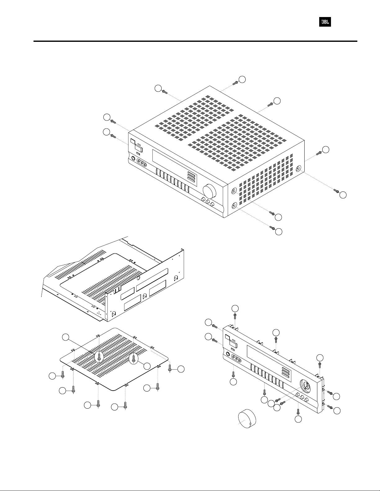
JBL
DISASSEMBLY PROCEDURES
STEP 1.
REMOVING THE TOP COVER
1. REMOVING THE SCREWS 1~9
7
8
9
J
B
L
6
5
4
3
STEP 2.
REMOVING THE BOTTOM COVER
1. REMOVING THE SCREWS 1~8
8
1
2
3
4
2
1
STEP 3.
REMOVING THE FRONT PANEL
1. REMOVING KNOB VOLUME MAIN FROM FRONT PANEL
2. REMOVING THE SCREWS 1~12
3
2
11
10
4
5
6
9
7
8
J
B
1
7
6
L
12
5
KNOB VOLUME MAIN
10
Page 11
Dolby Pro-LogicÒA/V Receiver JSR-400
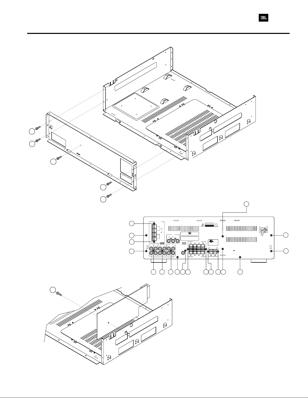
DISASSEMBLY PROCEDURES (continued)
STEP 4.
REMOVING THE FRONT CHASSIS
1. REMOVING THE SCREWS 1~5
1
2
3
4
5
STEP 6.
REMOVING THE TUNER PCB
1. REMOVING THE SCREWS 1
1
STEP 5.
REMOVING THE REAR PANEL
1. REMOVING THE SCREWS 1~18
1
2
3
4
ANTENNA
BAL
300W
FM
UNBAL
75W
VIDEO
GND
AM
IN
LOOP
AUX CD
TAPE
ININ
L
R
AUDIO
7
6
5
MODELNO. : JSR-400
DOLBYPROLOGIC RECEIVER
VCR1
MONITOR
OUT
OUT
Northridge,CAUSA
H
AHAarman International Company
VCR1
OUTINOUTIN
SUB
WOOFER
9
8
10
MAINSPEAKERS
R L
R L
REARSPEAKERS (8W)
CAUTION
!
RISKOF ELECTRIC SHOCK
DONOTOPEN.
AVIS: RISQUE DE CHOC
ELECTRIQUE-NEPAS OUVRIR
WARNING: "TO REDUCE THE RISK OF FIRE OR
ELECTRICSHOCK.
DONOT EXPOSE THISAPPLIANCE TO
RAINOR MOISTURE".
AVERTISSEMENT: "AFIN D'EVITER LES DANGERS
D'INCENDIEET D'ELECTROCUTION,
NEPAS EXPOSER CET APPPAREIL
ALA PLUIE NI A L'HUMIDITE".
(8W)
R
E28241
A172
Listed
Audioequipment
CENTER
SPEAKERS
(8W)
12 13 14 15
11
Thisdevices complies with Part 15 of the FCC rules. Operation is subject to the following
twoconditions; (1) The device may not cause harmful interferance, and (2) This device
mustaccept any interference received, including interference that may cause undesired
operation.
Manufacturedunder license from Dolby Laboratories Licensing Copration."Dolby,"the
double-Dsymbol and"Pro Logic" are trademarks of Dolby Laborotories Liencing
Coporation.
18
AC~120V60Hz
180W
17
16
11
Page 12

Dolby Pro-LogicÒA/V Receiver JSR-400
DISASSEMBLY PROCEDURES (continued)
4
1
3
2
STEP 7.
REMOVING THE POWER PCB
1. REMOVING THE SCREWS 1~4
STEP 8.
REMOVING THE VIDEO PCB
1. REMOVING THE SCREWS 1~2
STEP 9.
REMOVING THE MAIN PCB
1. REMOVING THE SCREWS 1~3
1
2
3
2
1
12
Page 13
Dolby Pro-LogicÒA/V Receiver JSR-400
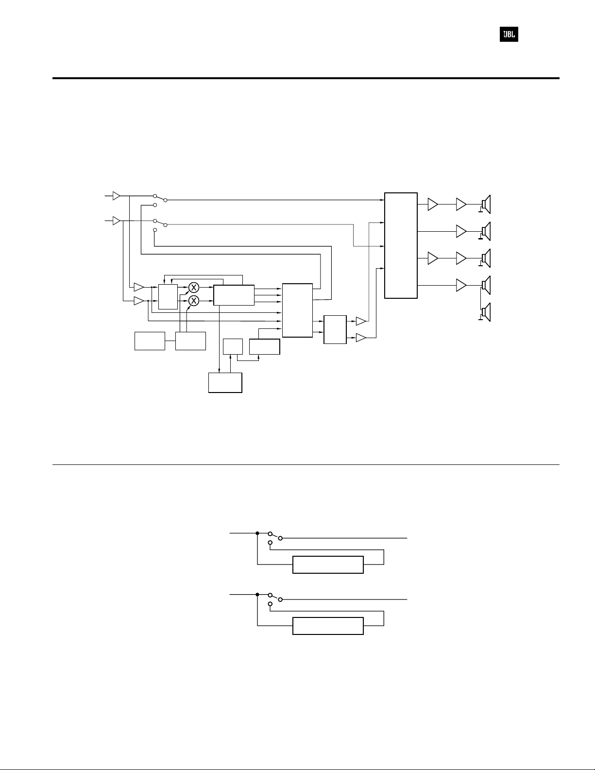
CIRCUIT DESCRIPTION
1. Surround Circuits
This model incorporates a surround processor circuit.
Fig. 1 is a block diagram of the surround processor circuit. The microprocessor transfers the data to the Dolby Pro-Logic
decoder and Time Delay Device to operate the circuits in each mode.
L Input
R Input
Buffer
Buffer
IC5
LC4966
IC10
NJW1102
X1
X1
Noise
Generator
Input
Autobalance
Control
Noise
Sequencer
IC11
NJU9702
S
VLRV
Adaptive
Matrix
S
By-Pass Line
7knz
LPF
Time
Delay
CS
Modified
Dolby B NR
L
C
R
MASTER
VOLUME
S
L
R
C
Center/
Operating
Mode
C
Control
S
electric
S
vol.
AMP
C
AMP
S
Fig. 1
TONE
CONTROL
TONE
CONTROL
AMP
AMP
AMP
AMP
Block diagram of the surround
processor circuit
1) BYPASS
Set to this mode to listen to ordinary stereo sound. The rear L/R and center outputs will be muted.
SPEAKER
FRONT L
CENTER
FRONT L
SURROUND L
SURROUND L
Fig. 2
SOURCE
L
SOURCE
R
IC5
LC4966
OUTPUT
SURROUND
OUTPUT
SURROUND
13
Page 14

Dolby Pro-LogicÒA/V Receiver JSR-400
2) DOLBY PRO-LOGIC CIRCUIT
Dolby Pro-Logic is a sound effect system for movies developed by the Dolby Laboratories Licensing Corp. IC10 (NJW1102) is
a Dolby Pro-Logic decoder IC. When an audio signal recorded using the Dolby Pro-Logic system is sent to this IC, the left,
right, center and surround components are separated. The surround signal component is delayed by the delay IC11
(NJU9702). Fig. 3 shows the configuration of the Dolby decoder.
IC10
V
LR
V
CS
By-Pass Line
7knz
LPF
L
R
C
S
Modified
Dolby B NR
Center/
Operating
Mode
Control
L-ch
R-ch
AMP
C
electric
S
vol.
C
AMP
S
C-ch
C-ch
Fig. 3
Audio
Signal
Audio
Signal
L-ch
R-ch
X1
X1
Input
Autobalance
Control
Flow of signals within the system
in the Dolby Pro-Logic mode
Adaptive
Matrix
S
IC11
NJU9702
Time
Delay
With Dolby Pro-Logic, three center modes depend on the use of a center speaker as follows.
NORMAL: Bass frequencies are sent only to the Left and Right Front channels. Select this mode when the
Center Speaker is smaller than the left and Right speakers.
WIDE: Bass frequencies are sent to the Left, Center and Right speakers. Select this mode when the
Center speaker is approximately the same size as the Left and Right speakers.
PHANTOM: Center channel information is sent to the Left and Right speakers. Select this mode when you do
not have a center channel speaker.
3) STEREO CIRCUIT
In 3-stereo mode, surround sound is sent to front Left channel and front Right channel and no surround sound is sent to
surround channel.
S
Fig. 4
IC10 NJW1102
Audio
L-ch
Signal
Audio
R-ch
Signal
Flow of signal within the system in the 3-stereo mode
X1
X1
Input
Autobalance
Control
Adaptive
Matrix
L
Center/
R
Operating
Mode
C
Channel
C
electric
vol.
L-ch
R-ch
C-ch
14
Page 15

Dolby Pro-LogicÒA/V Receiver JSR-400
4) TEST TONE GENERATOR
The test tone generator generates a test tone (noise) to check the balance of sound output from each speaker in the Dolby
Pro-Logic mode. (This circuit is produced under license of the Dolby Laboritories Licensing Corp.) The test tone to the
loudspeakers at 2 second intervals in the following sequence: Left, Center, Right, Rear (both rear channels).
Fig. 5
Flow of noise signals within the system
IC10 NJW1102
Input
AutoBalance
Control
Noise
Sequencer
Adaptive
Matrix
S
Time
Delay
IC11
NJU9702
2. DIGITAL TUNING SYSTEM DESCRIPTION.
1) DIGITAL TUNING SYSTEM
FM ANT
FM FRONT END PACK
L
B
Center/
C
Operating
Mode
Channel
S
FM PLL Loop
AM PLL Loop
L-ch
R-ch
Noise signal output
C-ch
S-ch
AM ANT
FM RF
AM RF
FM MIX
FM OSC
BUFFER
AM MIX
AM OSC
BUFFER
Low Pass Filter
Q201, 202
PLL Prescaler
FM IN
IC2
AM IN
Data
CPU
IC1
FL
Display
Key
Switch
Matrix
15
Page 16

Dolby Pro-LogicÒA/V Receiver JSR-400
2) VCO VS. FM BAND FREQUENCY CURVE.
8
7
6
5
CO
4
V Voltage (V)
3
2
1
0
87.5 89.5 91.5 93.5 95.5 97.5 99.5 101.5103.5 105.5 107.5
3) VCO VS. AM BAND FREQUENCY CURVE.
9
8
7
6
5
CO
4
V Voltage (V)
FM Band Frequency (MHz)
3
2
1
0
520 600 700 800 900 1000 1100 1200 1300 1400 1500 1600
AM Band Frequency (kHz)
16
Page 17
Dolby Pro-LogicÒA/V Receiver JSR-400
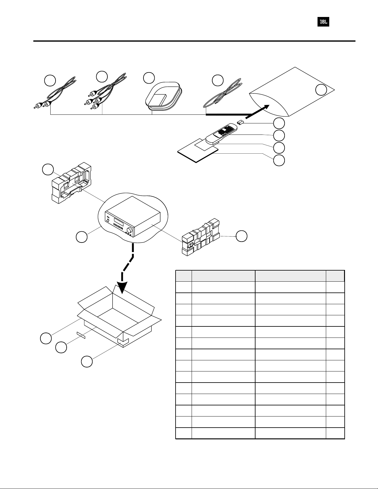
JSR400 PACKING
4
5
6
7
8
ATTACHED WITH
CELLOPHANE TAPE
9
10
11
12
3
2
3
NO.NO.
1
2
3
4
5
1
13
14
6
7
8
9
10
11
12
13
14
PARTS NO.
6121-000-421
6132-000-060
6161-000-140
2163-000-020
2163-000-010
6457-000-010
6452-000-020
6131-000-160
6453-000-002
6425-000-240
6231-001-011
1111-ARCCINII
6234-002-000
6234-001-021
PARTS NAME
MASTER CARTON
POLY SHEET
CUSHION SIDE
CORD PIN
CORD RCA
AM LOOP ANTENA
ANT. FM
BAG PE
BATTERY
REMOCON ASS'Y
CARD WARRANTY
INSTRUCTION MANUAL
LABEL SERIAL NO
LABEL BARCODE #39
QT'Y
1
1
2
1
1
1
1
1
2
1
1
1
1
1
17
Page 18

Dolby Pro-LogicÒA/V Receiver JSR-400
JSR400 BLOCK DIAGRAM
1
ANT
AUDIO
TUNER
TAPE
VCR1
VIDEO
CD
FM
AM
TV
BA
FM
FRONT END
AM
AM
OSC
ANT
I
O
I
O
I
C
F101
PLL IC
LM7001
IC2
F102
IC3
AM/FM IF
LA1265
AM
IF T
F202
IC7821
BUFFER
ED
IC4
FM MPX
LA3410
FM
DET
BY-PASS
F
DATA
CLK
CE
TUNED
STEREO
T-MUTE
L.P.F.
MASTER VOLUME
G
CPU
H
- INPUT PARTS
- SURROUND PARTS
- TUNER PARTS
- MAIN AMP PARTS
- POWER SUPPLY PARTS
I
FL DISPLAY
RIGHT CHANNEL
(SAME AS LEFT CHANNEL)
TONE AMP
14.5dB
BALANCE
J
RESORNATOR
FL AC 4V
+15V
-15V
+5V
FRONT AMP
CENTER AMP
REAR AMP
KEY MATRIX
CPU
REGULATOR
+15V. -15V.
+5V
AMP
POWER
SUPPLY
MAIN AMP
LMK
RMC
SENSOR
MAIN
POWER
TRANS
PROTECT
RELAY
DRIVER
COMMANDER
5V
REGU.
ST-BY RELAY
ST-BY
TRANS
O
EUROPE : 230/50Hz
USA : 120/60Hz
P
HEAD
PHONE
FRONT
SPEAKER
VIDEO
VCR
O
VIDEO IN
MONITOR
I
6dB AMP
6dB AMP
LC4966
VCR
VIDEO from CPU
JSR-400 BLOCK DIAGRAM
JSR-400 PAGE 18-1of2
ABCDE
F
DOLBY PRO-LOGIC
ADAPTIVE MATRIX
NJW1102
DIGITAL
DELAY
NJU9702
G
H
C-CH
S-CH
2.92dB
0.83dB
MUTE
SUB WOOFER
PROTECT
19.3dB
MUTE
MUTE
19.3dB
J
K
LMI
CENTER AMP
PROTECT
REAR AMP
JSR-400 PAGE 18-2of2
O
CENTER
SPEAKER
L
REAR
SPEAKER
R
P
18
Page 19

BA
T
C
E
N
E
A
T
C
ED
F
G
H
I
1
ANT
AUDIO
TUNER
TAPE
VCR1
VIDEO
CD
FM
AM
TV
F101
FM
FRONT END
IC3
AM/FM IF
AM
OSC
PLL IC
LM7001
IC2
AM
ANT
I
O
I
O
I
LA1265
AM
IF T
IC7821
F102
F202
BUFFER
IC4
FM MPX
LA3410
FM
DET
DATA
CLK
CE
TUNED
STEREO
T-MUTE
BY-PASS
CPU
L.P.F.
MASTER VOLUME
FL DISPLAY
- INPUT PARTS
- SURROUND PARTS
- TUNER PARTS
- MAIN AMP PARTS
- POWER SUPPLY PARTS
RIGH
(SAME AS
TONE AMP
14.5dB
BALAN
FL
FRO
CENT
RE
R
VIDEO
VCR
O
VIDEO IN
MONITOR
I
6dB AMP
6dB AMP
LC4966
VCR
VIDEO from CPU
JSR-400 BLOCK DIAGRAM
JSR-400 PAGE 18-1of2
ABCDE
F
DOLBY PRO-LOGIC
ADAPTIVE MATRIX
NJW1102
DIGITAL
DELAY
NJU9702
G
H
C-CH
S-CH
2.92dB
0.83dB
I
MU
Page 20

G
J
H
I
J
LMK
O
P
U
VOLUME
FL DISPLAY
- INPUT PARTS
- SURROUND PARTS
- TUNER PARTS
- MAIN AMP PARTS
- POWER SUPPLY PARTS
RIGHT CHANNEL
(SAME AS LEFT CHANNEL)
RESORNATOR
FL AC 4V
FRONT AMP
CENTER AMP
REAR AMP
BALANCE
+15V
-15V
+5V
KEY MATRIX
CPU
REGULATOR
+15V. -15V.
+5V
AMP
POWER
SUPPLY
RMC
SENSOR
MAIN
POWER
TRANS
PROTECT
RELAY
DRIVER
COMMANDER
5V
REGU.
ST-BY RELAY
EUROPE : 230/50Hz
USA : 120/60Hz
ST-BY
TRANS
HEAD
PHONE
PRO-LOGIC
IVE MATRIX
W1102
DIGITAL
DELAY
JU9702
TONE AMP
14.5dB
C-CH
S-CH
2.92dB
0.83dB
MUTE
MAIN AMP
19.3dB
MUTE
MUTE
19.3dB
CENTER AMP
REAR AMP
FRONT
SPEAKER
SUB WOOFER
PROTECT
CENTER
SPEAKER
PROTECT
L
REAR
SPEAKER
R
JSR-400 PAGE 18-2of2
G
H
J
K
LMI
O
P
Page 21
Dolby Pro-LogicÒA/V Receiver JSR-400
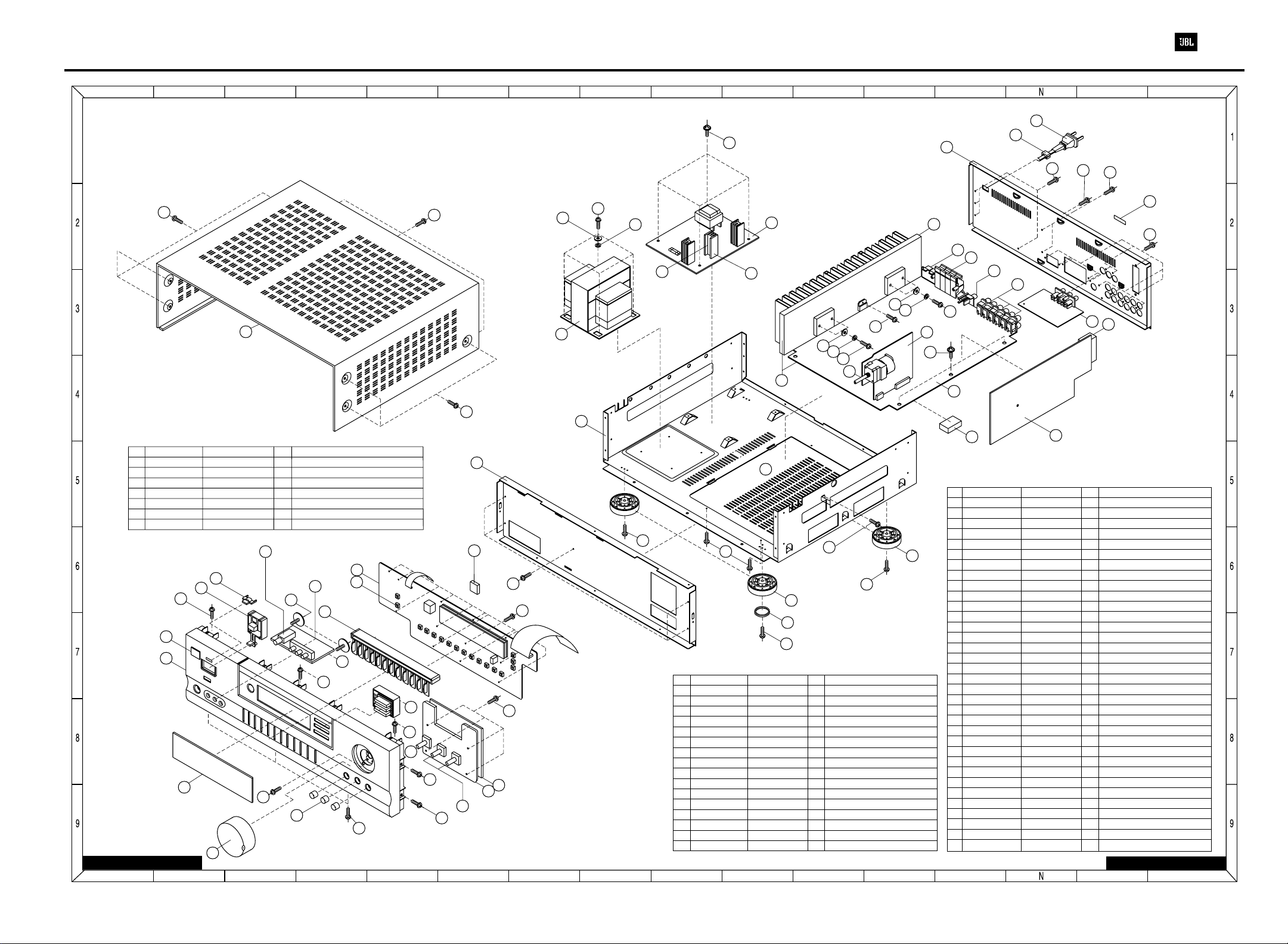
JSR-400 UNIT EXPLODED VIEW
1
JSR-400 Mechanical
Exploded View
S7
PARTS CODE
NO
1514-000-030
JK1
1515-000-011
JK2
1514-000-020
JK3
1514-000-021
JK4
1531-000-020
JK5
1531-000-021
JK6
1531-000-002
JK7
33
1
JSR-400 PAGE 19-1of2
ABCDE
BA
5
S1
JBL
2
C
28
PARTS NAME
JACK RCA
JACK PHONE
JACK RCA
JACK RCA
TERMINAL SPEAKER
TERMINAL SPEAKER
TERMINAL ANTENNA
JK2
3
S1
4
Q'TY
MATERIAL & SPECIFICATION
3P JW-3104D,GOLD,YWR JAEWON
1
HP 6.5H,3 ST,HTJ-064-08D,GOLD
1
1P JW-1512,BLACK, WAKA
1
4P JW-4104R, JAEWON
3
2P JW-5502A,JAEWON
1
8P JW-5508A, JAEWON
1
4P JW-5540D,JAEWON
1
8
JK1
SW1
S4
7
9
S1
12
S6
ED
F
G
H
I LMK
J
O
P
26
S8
S6
W2
S3
W1
30
24
27
25
S6
S6
S6
32
S6
JK5
JK6
S1
31
JK3
JK4
x3
W4
W3
29
W4
W3
S2 X3
S1
S5
VR1
S5
19
23
JK7
S8
20
6
S1
VR2
S7
14
13
S1
S1
S2
S1
11
10
VR3
S1
15
22
21
18
Q'TY
PARTS CODE
NO
1
5111-000-152
2
5514-000-061
3
5142-000-041
4
S1
S8
S1
16
S1
16
17
S1
NO
S1
S2
S3
S4
S5
S6
S7
S8
W1
W2
W3
W4
VR1
VR2
VR3
SW1
PARTS CODE
5636-130-080
5636-140-040
5636-140-080
5636-140-060
5636-140-030
5636-140-010
5636-140-130
5636-140-020
5541-001-030
5541-001-040
5541-001-010
5541-001-020
1723-503-002
1721-104-030
1721-104-040
1671-000-013
PARTS NAME
SCREW
SCREW
SCREW
SCREW
SCREW
SCREW
SCREW
SCREW
WASHER
WASHER
WASHER
WASHER
VOLUME MOTOR
VOLUME ROTARY
VOLUME ROTARY
SWITCH TACT
MATERIAL & SPECIFICATION
Q'TY
A123008000
40
A183008000
10
A124008000
4
S30C ( BTTN, D:12, 3X10)
2
A113016000
4
23
A123010002
A184008002
6
A123006000
8
WASHER SPRING;NO.2,M4.0,MC,TOYO
4
WASHER FLAT P/W 4.4*12*1.0,MC.TOYO
4
WASHER SPRING;NO.2,M3.0,MC,TOYO
4
WASHER FLAT P/W 3.3*8.0*0.5,MC.TOYO
4
RK16814MG 50KAX4 LG
1
RK14K1280307 100KMNX2 W/BUSHING LG
1
RK14K1280307 100KC X2 W/BUSHING LG
2
SW TACT KPT1105AM-1 4PIN
17
5131-001-172
5
5131-001-182
6
5131-001-222
7
5131-001-212
8
9
10
11
5226-000-210
12
5131-001-192
13
5441-000-120
5221-000-090
14
15
5221-000-080
5179-000-050
16
5141-000-110
17
18
5221-000-170
19
20
21
22
5441-000-131
23
24
5212-000-041
25
5179-000-060
2161-000-0032-1
26
27
5241-000-090
5213-000-022
28
1419-000-030J
29
1419-000-030-1
30
5241-000-110
31
6234-001-108
32
5351-000-900
33
PARTS NAME
PANEL FRONT
WINDOW FLT
LENS . LED
KNOB . VOLUME
BUTTON . POWER
BUTTON . TUNNING
BUTTON . FUNCTION
PCB
PCB
PCB
SHIELD CASE
KNOB . ROTARY
CUSHION FLT
CHASSIS . FRONT
CHASSIS . MAIN
FOOT FRONT
FOOT CUSHION
BOTTOM COVER
PCB
PCB
PCB
PCB
CUSHION PCB
PCB
REAR CABINET
BUSHING AC CORD
CORD POWER
HEAT SINK. MAIN
TOP COVER
POWER TRANS
POWER TRANS
PCB
HEAT SINK. PIN
LABEL
BADGE
MATERIAL & SPECIFICATION
1
HIPS
1
PVC T1.0 WINE COLOR
1
ACRYL
ABS
1
1
ABS
ABS
1
ABS
1
1
CONTROL (1X2)
SUB (JACK)
1
SUB (TONE)
1
SPTE T0.3
1
ABS
3
CUSHION H:25
2
SECC T1.0
1
1
SECC T1.0
4
ABS(H/STAMP:GOLD)+RUBBER
RUBBER
4
SECC 1.0t
1
SUB(VOLUME)
1
MAIN BOARD
1
1
TUNER PCB
3
TUNER PCB
SUB (REAR)
1
SECC 1.0T
1
NYLON 66 (NIFCO 2271)
1
UL , PT2
1
1
A6063-T5 AL.
SECC T0.6+PVC T0.2
1
120V 60HZ
1
230V/50HZ, VDE
1
SUB (POWER)
1
3
A6063-T5, PIN TYPE
1
MADE IN CHAINA
1
JBL
JSR-400PAGE19-2of2
F
G
H
J
K
LMI
O
P
19
Page 22

3
BA
C
ED
F
G
H
I
1
JSR-400 Mechanical
S8
Exploded View
W2
S3
W1
S1
15
S1
S8
PARTS CODE
NO
1514-000-030
JK1
1515-000-011
JK2
1514-000-020
JK3
1514-000-021
JK4
1531-000-020
JK5
1531-000-021
JK6
1531-000-002
JK7
S7
28
S6
29
S7
Q'TY
MATERIAL & SPECIFICATION
3P JW-3104D,GOLD,YWR JAEWON
1
HP 6.5H,3 ST,HTJ-064-08D,GOLD
1
1P JW-1512,BLACK, WAKA
1
4P JW-4104R, JAEWON
3
2P JW-5502A,JAEWON
1
8P JW-5508A, JAEWON
1
4P JW-5540D,JAEWON
1
8
JK1
SW1
S4
7
14
13
S1
S1
5
S1
PARTS NAME
JACK RCA
JACK PHONE
JACK RCA
JACK RCA
TERMINAL SPEAKER
TERMINAL SPEAKER
TERMINAL ANTENNA
JK2
3
33
JBL
1
9
S1
6
S1
VR2
2
S1
12
S1
VR3
S1
S6
4
JSR-400 PAGE 19-1of2
ABCDE
F
PARTS CODE
NO
5636-130-080
S1
5636-140-040
S2
5636-140-080
S2
11
10
G
H
S3
S4
S5
S6
S7
S8
W1
W2
W3
W4
VR1
VR2
VR3
SW1
5636-140-060
5636-140-030
5636-140-010
5636-140-130
5636-140-020
5541-001-030
5541-001-040
5541-001-010
5541-001-020
1723-503-002
1721-104-030
1721-104-040
1671-000-013
I
Page 23

G
H
I
J
LMK
O
P
26
S8
24
25
S6
S6
S6
32
W2
S3
W1
30
27
S6
JK5
JK6
S1
31
JK3
JK4
x3
W4
W3
29
W4
W3
S2 X3
S1
S5
VR1
S5
19
23
JK7
S8
20
15
22
21
18
PARTS CODE
NO
1
5111-000-152
2
5514-000-061
3
5142-000-041
4
S1
S8
S1
16
S1
16
17
S1
NO
S1
S2
S3
S4
S5
S6
S7
S8
W1
W2
W3
W4
VR1
VR2
VR3
SW1
PARTS CODE
5636-130-080
5636-140-040
5636-140-080
5636-140-060
5636-140-030
5636-140-010
5636-140-130
5636-140-020
5541-001-030
5541-001-040
5541-001-010
5541-001-020
1723-503-002
1721-104-030
1721-104-040
1671-000-013
PARTS NAME
SCREW
SCREW
SCREW
SCREW
SCREW
SCREW
SCREW
SCREW
WASHER
WASHER
WASHER
WASHER
VOLUME MOTOR
VOLUME ROTARY
VOLUME ROTARY
SWITCH TACT
MATERIAL & SPECIFICATION
Q'TY
A123008000
40
A183008000
10
A124008000
4
S30C ( BTTN, D:12, 3X10)
2
A113016000
4
23
A123010002
A184008002
6
A123006000
8
WASHER SPRING;NO.2,M4.0,MC,TOYO
4
WASHER FLAT P/W 4.4*12*1.0,MC.TOYO
4
WASHER SPRING;NO.2,M3.0,MC,TOYO
4
WASHER FLAT P/W 3.3*8.0*0.5,MC.TOYO
4
RK16814MG 50KAX4 LG
1
RK14K1280307 100KMNX2 W/BUSHING LG
1
RK14K1280307 100KC X2 W/BUSHING LG
2
SW TACT KPT1105AM-1 4PIN
17
5131-001-172
5
5131-001-182
6
5131-001-222
7
5131-001-212
8
9
10
11
5226-000-210
12
5131-001-192
13
5441-000-120
5221-000-090
14
15
5221-000-080
5179-000-050
16
5141-000-110
17
18
5221-000-170
19
20
21
22
5441-000-131
23
24
5212-000-041
25
5179-000-060
2161-000-0032-1
26
27
5241-000-090
5213-000-022
28
1419-000-030J
29
1419-000-030-1
30
5241-000-110
31
6234-001-108
32
5351-000-900
33
PARTS NAME
PANEL FRONT
WINDOW FLT
LENS . LED
KNOB . VOLUME
BUTTON . POWER
BUTTON . TUNNING
BUTTON . FUNCTION
PCB
PCB
PCB
SHIELD CASE
KNOB . ROTARY
CUSHION FLT
CHASSIS . FRONT
CHASSIS . MAIN
FOOT FRONT
FOOT CUSHION
BOTTOM COVER
PCB
PCB
PCB
PCB
CUSHION PCB
PCB
REAR CABINET
BUSHING AC CORD
CORD POWER
HEAT SINK. MAIN
TOP COVER
POWER TRANS
POWER TRANS
PCB
HEAT SINK. PIN
LABEL
BADGE
Q'TY
MATERIAL & SPECIFICATION
1
HIPS
1
PVC T1.0 WINE COLOR
1
ACRYL
ABS
1
1
ABS
ABS
1
ABS
1
1
CONTROL (1X2)
SUB (JACK)
1
SUB (TONE)
1
SPTE T0.3
1
ABS
3
CUSHION H:25
2
SECC T1.0
1
1
SECC T1.0
4
ABS(H/STAMP:GOLD)+RUBBER
RUBBER
4
SECC 1.0t
1
SUB(VOLUME)
1
MAIN BOARD
1
1
TUNER PCB
3
TUNER PCB
SUB (REAR)
1
SECC 1.0T
1
NYLON 66 (NIFCO 2271)
1
UL , PT2
1
1
A6063-T5 AL.
SECC T0.6+PVC T0.2
1
120V 60HZ
1
230V/50HZ, VDE
1
SUB (POWER)
1
3
A6063-T5, PIN TYPE
1
MADE IN CHAINA
1
JBL
JSR-400 PAGE 19-2of2
G
H
J
K
LMI
O
P
Page 24

Dolby Pro-LogicÒA/V Receiver JSR-400
JSR-400 ELECTRICAL PARTS LISTS
Ref # Part # Description Qty Ref # Part # Description Qty
ASS’Y-PCB MAIN JSR-400
Ref # Part # Description Qty
Transistors
Q1, 4, 5, 11, 12, 13 1243-319-001 TR-TAP TO-92 KTC3198 (C1815)-GR 6
Q2, 6, 7 1243-124-001 TR-TAP TO-92M KRC 103M KEC 3
Q3, 10 1244-126-001 TR-TAP TO-92 KTA1266(A1015)-Y KEC 2
Q8, 9 1244-124-001 TR-TAP TO-92M KRA103M KEC 2
Q15, 16, 21 1244-101-010 TR-TAP TO-92M KRA101M KEC 3
Q17, 18, 19, 20, 22 1243-130-003 TR-TAP TO-92 KTD1302 KEC 5
Diodes
D4, 6, 8, 9, 10, 11, 1252-000-001 D-SI TAP IN4148 (ISS131) 10
13, 14, 18, 19
Resistors
R1, 2, 3, 5, 8, 9, 1742-331-721 R-CARBON TAP 1/8W 330W± 5% 12
10, 12, 13, 14,
15, 16
R4, 47, 48, 95, 1742-104-721 R-CARBON TAP1/8W 100KW± 5% 7
128, 401, 402
R11, 42, 44, 45, 1744-470-731 R-CARBON TAP 1/4W 47W± 5% 10
46, 96, 108,
151, 152, 166
R17, 19, 310 1744-222-731 R-CARBON TAP 1/4W 2.2KW± 5% 3
R18, 20, 143, 144, 1742-102-721 R-CARBON TAP 1/8W 1KW± 5% 6
147, 148
R22, 35, 43, 79, 1744-103-731 R-CARBON TAP 1/4W 10KW± 5% 15
88, 89, 90, 99,
106, 133, 134,
192, 301, 500,
502
R23, 24, 25, 26, 1742-473-721 R-CARBON TAP 1/8W 47KW± 5% 10
52, 113, 116,
153, 156, 160
R27, 28, 68, 69 1744-272-731 R-CARBON TAP 1/4W 2.7KW± 5% 4
R29, 30 1744-473-731 R-CARBON TAP 1/4W 47KW± 5% 2
R31, 34, 54, 59, 97 1744-101-731 R-CARBON TAP 1/4W 100W± 5% 5
R32, 33, 41, 51, 1744-332-731 R-CARBON TAP 1/4W 3.3KW± 5% 8
55, 58, 64, 65
R37, 53, 72, 73, 1761-100-731 R-FUSIBLE/AX TAP 1/4W 10W± 5% 8
75, 76, 174, 403
R38, 49, 50 1744-154-731 R-CARBON TAP 1/4W 150KW± 5% 3
R39, 40, 56, 57, 1744-102-731 R-CARBON TAP 1/4W 1KW± 5% 12
62, 63, 77, 80,
110, 111, 112,
139
R60, 61, 66, 67, 71 1744-563-731 R CARBON TAP 1/4W 56KW± 5% 5
R70 1771-152-762 R-METAL/AX FORMING 1
R74, 136 1775-R27-782 R-CEMENT/AX FORMING 2
R78 1744-753-731 R-CARBON TAP 1/4W 75KW± 10% 1
R81 1771-100-752 R-METAL/AX FORMING 1W 10W± 5% 1
R82, 119, 120, 124 1744-223-731 R-CARBON TAP 1/4W 22KW± 5% 4
2W 1.5KW± 5%
5W 0.27W± 5%
R83, 84 1744-183-731 R-CARBON TAP 1/4W 18KW± 5% 2
R87 1744-683-731 R-CARBON TAP 1/4W 68KW± 5% 1
R91, 92, 93, 170, 1744-333-731 R-CARBON TAP 1/4W 33KW± 5% 6
171, 400
R98 1744-560-731 R-CARBON TAP 1/4W 56W± 5% 1
R100, 105, 114, 1742-153-721 R-CARBON TAP 1/8W 15KW± 5% 6
117, 125, 127
R102 1744-433-731 R-CARBON TAP 1/4W 43KW± 5% 1
R103, 104 1744-220-731 R-CARBON TAP 1/4W 22W± 5% 2
R107 1744-203-731 R-CARBON TAP 1/4W 20KW± 5% 1
R109 1744-105-731 R-CARBON TAP 1/4W 1MW± 5% 1
R115, 118 1742-752-721 R-CARBON TAP 1/8W 7.5KW± 5% 2
R121 1742-475-721 R-CARBON TAP 1/8W 4.7MW± 5% 1
R122 1742-224-721 R-CARBON TAP 1/8W 220KW± 5% 1
R123 1742-334-721 R-CARBON TAP 1/8W 330KW± 5% 1
R130 1744-562-731 R-CARBON TAP 1/4W 5.6KW± 5% 1
R131 1742-223-721 R-CARBON TAP 1/8W 22KW± 5% 1
R132, 146, 154 1742-103-721 R-CARBON TAP 1/8W 10KW± 5% 3
R145, 149, 150 1742-471-721 R-CARBON TAP 1/8W 470KW± 5% 3
R157, 159, 193 1742-472-721 R-CARBON TAP 1/8W 4.7KW± 5% 3
R158 1742-123-721 R-CARBON TAP 1/8W 12KW± 5% 1
R172, 173 1744-182-731 R-CARBON TAP 1/4W 1.8KW± 5% 2
R501 1742-332-721 R-CARBON TAP 1/8W 3.3KW± 5% 1
Capacitors
C1, 3, 30, 35, 36, 1862-470-404 C-ELEC/RA TAP 5*11 16V 47 UF ± 20% 12
37, 78, 85, 88,
111, 138, 140
C2, 4, 5, 6, 9, 10, 1832-101-822 C-CERA/AX TAP 50V Y5P 100pF ± 10% 20
11, 12, 13, 14,
15, 16, 22, 29,
51, 60, 74, 91,
92, 93
C18, 20, 77, 114, 1832-104-002 C-CERA/AX TAP 50V Y5V 0.1uF ± 10% 6
802, 902
C19, 21, 25, 48, 1862-100-504 C-ELEC/RA TAP 5*11 16V 10uF ± 20% 16
107, 108, 115,
116, 133, 135,
136, 141, 143,
706, 904, 905
C26 1862-101-706 C-ELEC/RA TAP 8*12 35V 100uF ± 20% 1
C27, 28, 64, 65, 71 1862-101-806 C-ELEC/RA TAP 8*12 50V 100uF ± 20% 5
C31, 32, 61, 63 1832-120-712 C-CERA/AX TAP 50V CH 12pF ± 5% 4
C33, 42 1832-221-822 C-CERA/AX TAP 50V Y5P 220pF ± 10% 2
C34, 109, 113 1862-220-504 C-ELEC/RA TAP 5*11 16V 22uF ± 20% 3
C38, 39, 40, 41, 1862-4R7-804 C-ELEC/RA TAP 5*11 50V 4.7uF ± 20% 6
122, 123
C43, 45, 50, 52, 1862-470-805 C-ELEC/RA TAP 6*11 50V 47uF ± 20% 6
54, 59
C44, 46, 47, 53, 1862-100-804 C-ELEC/RA TAP 5*11 50V 10uF ± 20% 6
55, 58
C56, 57, 128 1832-471-822 C-CERA/AX TAP 50V Y5P 470pF ± 10% 3
20
Page 25

Dolby Pro-LogicÒA/V Receiver JSR-400
Ref # Part # Description Qty Ref # Part # Description Qty
C66, 67, 82, 83, 1876-473-811 C-POLYESTER 100V 0.047uF ± 10% 9
94, 95, 125, 900,
908
C68 1862-330-804 C-ELEC/RA TAP 6*11 50V 33 UF ± 20% 1
C69, 709, 710 1862-010-804 C-ELEC/RA TAP 5*11 50V 1.0uF ± 20% 3
C70 1862-471-306 C-ELEC/RA TAP 8*12 10V 470uF ± 20% 1
C79, 87 1832-561-822 C-CERA/AX TAP 50V Y5P 560pF ± 10% 2
C80 1832-222-983 C-CERA/AX TAP 16V Y5R 1
C81, 84, 96, 97, 134 1876-104-811 C-POLYESTER 100V 0.1uF ± 10% 11
100, 102, 103,
105, 106, 117,
C86, 126 1832-562-983 C-CERA/AX TAP 16V Y5R 2
C89, 90 1832-330-772 C-CERA/AX TAP 50V SL 33pF ± 5% 2
C98, 99 1876-223-811 C-POLYESTER 100V 0.022uF ± 10% 2
C101, 104 1832-681-822 C-CERA/AX TAP 50V Y5P 680pF ± 10% 2
C110 1862-101-504 C-ELEC/RA TAP 5*11 16V 100uF ± 20% 1
C112 1876-332-811 C-POLYESTER/RA TAP 100V 1
C118, 119, 120, 121 1875-224-811 C-POLYESTER/RA STD 100V 4
C124 1862-R68-804 C-ELEC/RA TAP 5*11 50V 0.68uF ± 20% 1
C129 1832-182-983 C-CERA/AX TAP 16V Y5R 1
C130 1862-221-305 C-ELEC/RA TAP 6*11 10V 220uF ± 20% 1
C142, 144 1862-R47-804 C-ELEC/RA TAP 5*11 50V 0.47uF ± 20% 2
C800, 801 1861-682-820 C-ELEC/RA 30*60 50V 6800uF ± 20% 2
C910, 911, 912, 1832-104-822 C-CERA/AX TAP 50V Y5V 6
913, 914, 915
C916 1832-472-983 C-CERA/AX TAP 16V Y5R 1
0.0022uF ± 20%
0.0056uF ± 20%
0.0033uF ± 10%
0.22uF ± 10%
0.0018uF ± 20%
0.1uF + 80%, -20%
0.0047uF ± 10%
Integrated Circuits
IC1 1212-782-025 LC7821 FUNCTION SELECTOR 1
IC2, 3 1211-419-001 IC-SIP STK4192II HIGH POWER AMP 2
IC4, 13 1212-455-001 IC-DIP NJM4558DD OP AMP JRC 2
IC5 1212-496-001 QUAD BILATERAL SWITCH 1
IC10 1212-110-001 IC-DIP NJW1102L D/S DECODER JRC 1
IC11 1212-970-001 IC-DIP NJU9702D D/S DELAY JRC 1
SANYO
Diodes
D7, 21 1252-000-005J D-RECT TAP 100V 1A IN4002 M.D 2
D20 1253-000-010 D-BRIDGE 400V 6A KBU602 1
Miscellaneous
X1 1341-000-051 FIL-RESONATOR ZTA2.0MHZ CQ 1
L1, 2, 3, 4 1451-000-030 COIL-AF CHOKE 2UEW 0.9F 4
JACK3 1514-000-020 JACK-RCA 1P JW-1512 BLK WAKA 1
JACK13, 14, 15 1514-000-021 JACK-RCA 4P JW-4104R JAEWON 3
ID 10 0.7uH
SP3 1531-000-020 TERMINAL-PUSH 2P JW-5502A 1
SP 4 1531-000-021 TERMINAL-PUSH 8P JW-5508A 1
FU1 1541-5R0-001-1 FUSE 5 x 20mm 250V 5A UL 1
PO1 1782-000-001 R-POSISTOR P42T8D100B04 1
RY7 2022-000-001 RELAY DC24V 2CIP DG2SU DAI ICHI 1
WA1, 4 2111-023-005 CON-WAFER 5267-0 5A 5P P=2.5 2
WA2 2111-023-003 CON-WAFER 5267-03A 3P P=2.5 1
WA3 2111-021-014J CONNECTOR-WAFER 2253-14P-T 1
WA8 2111-026-003 CONNECTOR-WAFER 3P P=3.96 1
WA10 2111-023-009 CON-WAFER 5267-09A 9P P=2.5 1
WA11 2111-021-008 CONNECTOR-WAFER 2253-08P-T 1
WA12 2111-021-012 CONNECTOR-WAFER 2253-12P-T 1
CN2 2113-004-026 CONNECTOR-FFC:26P 1
T1 2141-010-100 CONNECTOR-ASS’Y 1PM AWG22M 1
5241-000-090 HEAT-SINK AL RV-50 YONGBI 1
5541-001-010 WASHER SPRING ;NO 2 4
5541-001-020 WASHER PLAT P/W 3.3*8.0*0.5 MC 4
5636-130-080 SCREW-TAP BH 3*8.0 FZY 1
5636-140-030 SCREW A113016000 TOYO 4
5636-140-040 SCREW A183008000 TOYO 3
PCB ASSY A0112-002-151-3 MAIN PCB FULLY LOADED 1
JAEWON
JAEWON
MOLEX
MOLEX
PLUG ILSAN
35313-0310 MOLEX
MOLEX
PLUG ILSAN
PLUG ILSAN
008370-261-000-800 ELCO KOR
250MM UL1672
M3.0MC TOYO
TOYO
A123008000 TOYO
ASS’Y PCB CONTROL JSR-400
Transistors
Q1 1243-319-001 TR-TAP TO-92 KTC3198(C1815)-GR 1
Diodes
D8, 10, 102, 1252-000-001 D-SI TAP IN4148(ISS131) 9
105-110
Resistors
R1 1742-102-721 R-CARBON TAP 1/8W 1KW± 5% 1
R2, 3, 4, 5, 22 1742-473-721 R-CARBON TAP 1/8W 47KW± 5% 5
R6, 9 1742-105-721 R-CARBON TAP 1/8W 1MW± 5% 2
R7 1744-4R7-731 R-CARBON TAP 1/4W 4.7W± 5% 1
R10 1744-100-731 R-CARBON TAP 1/4W 10W± 5% 1
R14, 15, 16 1742-103-721 R-CARBON TAP 1/8W 10KW± 5% 3
21
Page 26

Dolby Pro-LogicÒA/V Receiver JSR-400
Ref # Part # Description Qty Ref # Part # Description Qty
R18, 19, 20, 24, 25 1742-104-721 R-CARBON TAP 1/8W 100KW± 5% 5
R21 1744-221-731 R-CARBON TAP 1/4W 220W± 5% 1
R23 1742-221-721 R-CARBON TAP 1/8W 220W± 5% 1
Capacitor
C1 1862-R47-804 C-ELEC/RA TAP 5*11 50V 0.47uF ± 20% 1
C2 1862-470-404 C-ELEC/RA TAP 5*11 16V 47uF ± 20% 1
C4, 5 1862-R22-804 C-ELEC/RA TAP 5*11 50V 0.22uF ± 20% 2
C6, 7, 8 1832-331-822 C-CERA/AX TAP 50V Y5P 330pF ± 20% 3
C10 1832-223-001 C-CERA 25V Y5V 0.022uF +80%, -20% 1
C11 1881-000-010 C-GOLD 5.5V 0.047F SCDA5R5473V 1
C12, 22, 24, 25 1832-104-002 C-CERA/AX :TAP 50V Y5V 0.1uF 5
Rfre +80%, -20%
SAMSUNG
Integrated Circuits
IC1 1212-827-002 IC-DIP CXP82712-120S CPU SONY 1
Miscellaneous
RMC1 1264-000-021 SENSOR-REMOTE CRVIM352-B 1
LED 1 1271-000-019 LED RED 3 SLR34VT3 ROH 1
FLT 1 1277-000-010 FLT CM1558D RV-50 NORITAKE 1
X1 1341-000-080 FIL-RESONATOR ZTT10MHZ CQ 1
SW19 29-39 40-44 1671-000-013 SW-TACT KPT1105AM-1 4PIN 17
CN102 2113-004-026 CONNECTOR-FFC 26P 1
CN101 2141-050-070 CNT-ASS’Y 5P 400MM WOOCHANG 1
FLT 5441-000-120 CUSHION-FLT EVA BLK 5*25*120 1
PCB ASSY A0112-001-191 CONTROL PCB FULLY LOADED 1
38KHZ SAM YOUNG
008370-261-000-800 ELCO KOR
BEOMHWAN
RV-50
ASS’Y-PCB TUNER JSR-400
Transistors
Q101, 102 1243-319-008 TR-TAP TO-92 KTC3192-0 KEC 2
Q103, 302, 403 1244-101-010 TR-TAP TO-92M KRA101M KEC 3
Q201 1243-320-001 TR-TAP TO-92 KTC3200-GR KEC 1
Q202 1248-246-001 FET-TAP TO-92 2SK246-Y TOSHIBA 1
Q401, 402 1243-319-001 TR-TAP TO-92 KTC3198(C1815)-GR 2
Diodes
D302, 303, 402 1252-000-001 D-SI TAP IN4148( 1SS131) 3
ZD401 1254-5R6-009 D-ZENER TAP 0.5W 5.6V 1
Resistors
R14, 100, 412, 318 1744-101-731 R-CARBON TAP 1/4W 100W± 5% 4
R101, 418, 419 1742-101-721 R-CARBON TAP 1/8W 100W± 5% 3
MTZJ5.6B ROHM
R102 1742-122-721 R-CARBON TAP 1/8W 1.2KW± 5% 1
R103, 308 1742-222-721 R-CARBON TAP 1/8W 2.2KW± 5% 2
R104, 205, 206, 1742-331-721 R-CARBON TAP 1/8W 330W± 5% 5
333, 564
R105 1742-121-721 R-CARBON TAP 1/8W 120W± 5% 1
R106 1742-391-721 R-CARBON TAP 1/8W 390W± 5% 1
R107 1742-392-721 R-CARBON TAP 1/8W 3.9KW± 5% 1
R201, 304, 305, 1742-103-721 R-CARBON TAP 1/8W 10KW± 5% 5
444, 411
R202, 307, 401, 1742-102-721 R-CARBON TAP 1/8W 1KW± 5% 5
311, 317
R203, 316, 407, 408 1742-332-721 R-CARBON TAP 1/8W 3.3KW± 5% 4
R204, 207, 562 1742-221-721 R-CARBON TAP 1/8W 220W± 5% 3
R301, 302 1742-473-721 R-CARBON TAP 1/8W 47KW± 5% 2
R306 1742-153-721 R-CARBON TAP 1/8W 15KW± 5% 1
R312 1742-683-721 R-CARBON TAP 1/8W 68KW± 5% 1
R313 1742-560-721 R-CARBON TAP 1/8W 56W± 5% 1
R314 1742-223-721 R-CARBON TAP 1/8W 22KW± 5% 1
R315, 403, 404 1742-562-721 R-CARBON TAP 1/8W 5.6KW± 5% 3
R405, 406 1742-182-721 R-CARBON TAP 1/8W 1.8KW± 5% 2
R413, 416 1742-104-721 R-CARBON TAP 1/8W 100KW± 5% 2
R414, 415 1742-124-721 R-CARBON TAP 1/8W 120KW± 5% 2
R417 1744-221-731 R-CARBON TAP 1/4W 220W± 5% 1
R438 1742-393-721 R-CARBON TAP 1/8W 39KW± 5% 1
R441 1744-220-731 R-CARBON TAP 1/4W 22W± 5% 1
R556, 557, 558 1742-471-721 R-CARBON TAP 1/8W 470W± 5% 3
R565 1744-470-731 R-CARBON TAP 1/4W 47W± 5% 1
Capacitor
C21, 23, 404 1862-3R3-804 C-ELEC/RA TAP 5*11 50V 3.3uF ± 20% 3
C39 1832-103-483 C-CERA/AX TAP 16V Y5S 0.01uF ± 20% 1
C103, 317, 419, 1862-470-404 C-ELEC/RA TAP 5*11 16V 47uF ± 20% 5
421, 428
C104, 302, 303, 1832-223-001 C-CERA/AX TAP 25V Y5V 14
307, 308, 312, 0.022uF +80%, -20%
316, 416, 422,
434, 436, 437,
318, 450
C201 1876-102-811 C-POLYESTER 100V 0.001uF ± 10% 1
C202 1862-010-804 C-ELEC/RA TAP 5*11 50V 1.0uF ± 20% 1
C203, 204 1832-220-772 C-CERA/AX TAP 50V SL 22pF ± 5% 2
C306, 313, 401, 1862-100-504 C-ELEC/RA TAP 5*11 16V 10uF ± 20% 4
412
C314 1862-4R7-804 C-ELEC/RA TAP 5*11 50V 4.7uF ± 20% 1
C322 1875-154-811 C-POLYESTER STD 100V 0.15uF ± 10% 1
C323, 324 1832-473-001 C-CERA/AX TAP 25V Y5V 2
C402, 441 1862-R47-804 C-ELEC/RA TAP 5*11 50v 0.47uF ± 20% 2
C405, 417, 418, 1862-2R2-804 C-ELEC/RA TAP 5*11 50V 2.2uF ± 20% 5
430, 431
0.047uF + 80%, -20%
22
Page 27

Dolby Pro-LogicÒA/V Receiver JSR-400
Ref # Part # Description Qty Ref # Part # Description Qty
C413, 414 1832-681-822 C-CERA/AX TAP 50V Y5P 680pF ± 10% 2
C403 1876-473-811 C-POLYESTER/RA TAP 100V 1
C438 1872-471-731 C-STYROL/TAP 50V 470pF ± 5% 1
C452 1832-104-822 C-CERA/AX TAP 50V 0.1uF ± 10% 1
0.047uF ± 10%
Integrated Circuits
IC 2 1212-700-001 IC-DIP LM7001 PLL SANYO 1
IC 3 1212-126-001 IC-DIP LA1265 AM/FM IF SANYO 1
IC 4 1212-341-001 IC-DIP LA3410 FM MPX SANYO 1
Miscellaneous
VC1, 2 1252-000-040 D-VVC AM SVC321 SPA-D2 SANYO 2
PACK1 1291-000-011 TUNER PACK FM 87.5-108MHZ 1
F101, 102 1321-000-0051 FILTER-CERAMIC 2
F202 1321-000-0200 FILTER-CERAMIC :A450BL TOKO 1
F401 1341-000-0151 FIL-RESONATOR ZTB456F11CQ 1
F3 1341-000-060 FIL-RESONATOR LZU450C4N CQ 1
X2 1352-000-015J X-TAL HC-49/U 7.2MHZ 20PPM CQ 1
T4 1422-000-050 IFT-INSERT 7.5MM FD BLUE 1
T2 1422-000-060 IFT-INSERT 7.5MM AA WHT 1
T1 1432-000-040 COIL-INSERT 7.5MM AM ANT BLK 1
T6 1432-000-050 COIL-INSERT 7.5MM AO RED 1
L202 1444-3R3-002 INDUCTOR-AX TAP 3.3uH 1
ANT1 1531-000-003 TERMINAL-PUSH 4P JW-5504DB FCC 1
VR 301 302 1731-103-011 “VR-SEMI 6f , EVNDJAA0.3B14, 2
VR 401 1731-224-002 VR-SEMI 6f EVNDJAA03BE5 1
CT1, 2 1815-020-001J C-TRIM 6f NPO 20pF CV05-C200-1 2
WA2 2111-023-002 CON-WAFER 5267-02A 2P P=2.5 1
WA5 2111-020-012 CONNECTOR-WAFER 2253-12S-T 1
9961-000-001 PUSH TERMINAL EARTH PIN 1
ESD 1 2 D6854DMSA001 DIODE SCHOTTKY 2
PCB ASSY A0112-002-181-3 TUNER PCB FULLY LOADED 1
KST-F701VA-3 KWANGSUNG
SFE10.7MA5-A(RED) CQ
KWANGSUNG
KWANGSUNG
KWANGSUNG
KWANGSUNG
TLAP02KR3R3K
JAEWON
10K MASTSUSHITA”
220K 0hm MASTSUSHITA
CHUNNIL
MOLEX
SOCKET ILSAN
ASS’Y-PCB HEADPHONE JSR-400
Resistors
R52, 53 1771-681-752 R-METAL/AX FORMING 1W 680W± 5% 2
R82 1742-750-721 R-CARBON TAP 1/8W 75W± 5% 1
R83, 84 1742-331-721 R-CARBON TAP 1/8W 330W± 5% 2
Capacitor
C77, 81, 84 1832-104-002 C-CERA 50V Y5V 0.1uF +80%, -20% 3
C80 1862-330-504 C-ELEC 5*11 16V 33uF ± 20% 1
C82, 83 1832-101-822 C-CERA 50V Y5P 100pF ± 10% 2
Miscellaneous
JA1 1514-000-080 JACK-RCA 3P JW-3104D GOLD 1
JACK3 1515-000-011 JACK-H/P 6.3 ST HTJ-064-08D GOLD 1
CN5 2141-030-050 CNT-ASS’Y 3P 650MM WOOCHANG
CN10 2141-050-040 CNT-ASS’Y 5P 650MM W00CHANG 1
PCB ASSY A0112-001-1620 HEADPHONE PCB FULLY LOADED 1
Y/W/R JAEWON
BEOMHWAN
BEOMHWAN
ASS’Y PCB POWER SUPPLY JSR-400
Transistor
Q7 1243-319-001 TR-TAP TO-92 KTC3198 (C1815)-GR 1
Diodes
D11 1252-000-001 D-SI TAP IN4148 (ISS131) 1
DZ2 1254-012-033 D-ZENER TAP 0.5W 12V MTZJ12B 1
DZ3 1254-5R1-021 D-ZENER TAP 0.5W 5.1V MTZJ5.1B 1
Resistors
R38, 39, 46, 47, 81 1771-100-752 R-METAL/AX FORMING 1W 10W± 5% 5
R40, 44, 45 1744-102-731 R-CARBON TAP 1/4W 1KW± 5% 3
R41 1749-335-741 R-CARBON TAP 1/2W 3.3MW± 5% 1
R42 1744-331-731 R-CARBON TAP 1/4W 330W± 5% 1
R43 1744-104-731 R-CARBON TAP 1/4W 100KW± 5% 1
R80 1744-221-731 R-CARBON TAP 1/4W 220W± 5% 1
Capacitor
C25, 26, 41, 42, 79 1862-220-504 C-ELEC/RA TAP 5*11 16V 22uF ± 20% 5
C27, 28, 29 1862-470-705 C-ELEC/RA TAP 6*11 35V 47uF ± 20% 3
C31 1862-221-606 C-ELEC 8*11.5 25V 220uF ± 20% 1
C34 1832-104-822 C-CERA/AX TAP 50V 0.1uF ± 10% 1
C35 1825-000-010 C-DISC/AC AC250V 0.0047uF ± 20% 1
C36 1861-471-608 C-ELEC/RA 10*16 25V 470uF ± 20% 1
C39, 40 1861-222-610 C-ELEC/RA 16*25 25V 2200uF ± 20% 2
C78 1862-100-804 C-ELEC/RA TAP 5*11 50V 10uF ± 20% 1
C88 1825-104-000 C-AC 335M4104(0.1uF 275V) 1
ROHM
ROHM
SEMKO UL/CSA
SEMKO UL/CSA PILKOR
23
Page 28

Dolby Pro-LogicÒA/V Receiver JSR-400
Ref # Part # Description Qty Ref # Part # Description Qty
Integrated Circuits
IC5, 9 1217-780-001 IC-TO220i +6V 1A 7806 REGULATOR 2
IC6 1217-781-001 IC-TO220i +15V 1A 7815 REGULATOR 1
IC7 1217-791-001 IC-TO220i -15V 1A 7915 REGULATOR 1
Diodes
D2-10, 17-20 1252-000-005J D-RECT TAP 100V 1A IN4002 13
DZ1 1254-027-001 D-ZENER TAP 1W UZP-27B 1
Miscellaneous
TRAN1 1411-000-020J TRANS-SUB EI -35X14 120/60 UL 1
FU1, 2 1541-1R6-013-1 FUSE 5 x 20mm T/L 250V 1.6A UL 2
FU3 1541-315-020-1 FUSE 5 x 20mm T/L 250V 315mA UL 1
FU4 1541-5R0-001-1 FUSE 5 x 20mm NM 250V 5A UL 1
FU1, 2, 3, 4 1551-000-010 HOLDER-FUSE 5 8
RY1 2022-000-010 RELAY DC12V ICIP DGIU DA11CH1 1
WA1 2111-023-005 CON-WAFER 5267-05A 5P P=2.5 1
WA2 2111-026-004 CONNECTOR-WAFER 4P P=3.96 1
WA3 2111-026-002 CONNECTOR-WAFER 2P P=7.92 1
WA4 2111-026-002J CONNECTOR-WAFER 2P P=7.92 1
WA5 2111-026-003 CONNECTOR-WAFER 3P P=3.96 1
CN11 2141-090-030 CNT-ASS’Y 9P 450MM P=2.5 1
5241-000-110 HEAT-SINK AL6063S-T5 W/PIN 3
5636-130-080 SCREW-TAP BH 3*8.0 FZY 3
PCB ASSY A0112-001-1616 POWER SUPPLY PCB FULLY LOADED 1
MOLEX
35313-0410 MOLEX
35328-0210 MOLEX
JE202A-1T JAEEUN
35313-0310 MOLEX
WOOCHANG BEOMHWAN
L:40MM RV-50 YONGBI
A123008000 TOYO
ASS’Y PCB TONE JSR-400
Resistors
R60, 63 1742-223-721 R-CARBON TAP 1/8W 22KW± 5% 2
R61, 62, 66, 67, 1742-104-721 R-CARBON TAP 1/8W 100KW± 5% 6
71, 75
R65, 68 1742-392-721 R-CARBON TAP 1/8W 3.9KW± 5% 2
R70, 73 1742-222-721 R-CARBON TAP 1/8W 2.2KW± 5% 2
R72, 74 1742-102-721 R-CARBON TAP 1/8W 1KW± 5% 2
R77, 79 1742-821-721 R-CARBON TAP 1/8W 820W± 5% 2
Capacitor
C47, 52 1876-153-811 C-POLYESTER 100V 0.015uF ± 10% 2
C48, 53 1876-823-811 C-POLYESTER 100V 0.082uF ± 10% 2
C49, 60 1832-680-772 C-CERA/AX TAP 50V SL 68pF ± 5% 2
C50, 55 1832-101-822 C-CERA/AX TAP 50V Y5P 100pF ± 10% 2
C51, 56, 59, 62 1862-4R7-804 C-ELEC 5*11 50V 4.7uF ± 20% 4
C54, 57 1862-220-504 C-ELEC 5*11 16V 22uF ± 20% 2
C58, 61 1876-332-811 C-POLYESTER 100V 0.0033uF ± 10% 2
C63, 64 1876-183-811 C-POLYESTER 100V 0.018uF ± 10% 2
Integrated Circuits
IC8 1212-455-001 IC-DIP NJM4558DD OP AMP JRC 1
Miscellaneous
CN6 2141-050-050 CNT-ASS’Y 5P SHIELD 200MM 1
CN7 2141-030-040 CNT-ASS’Y 3P 200MM WOOCHANG 1
VR4 1721-104-030 VR-ROTARY 14MM, RK14K1280307 1
VR2, 3 1721-104-040 VR-ROTARY 14MM 2
5222-002-010 CASE-SHIELD SPTE 0.3t RV-50 1
PCB ASSY A0112-001-1618 TONE PCB FULLY LOADED 1
WOOCHANG BEOMHWAN
BEOMHWAN
100K W , W/BUSH LG
RK14K1280307100K W ALPS
ASS’Y PCB VOLUME JSR-400
Resistors
R2 1744-4R7-731 R-CARBON TAP 1/4W 4.7W± 5% 1
R3 1742-103-721 R-CARBON TAP 1/8W 10KW± 5% 1
R4 1744-562-731 R-CARBON TAP 1/4W 5.6KW± 5% 1
R6, 7, 16, 17 1742-473-721 R-CARBON TAP 1/8W 47KW± 5% 4
R8, 9, 14, 15 1742-104-721 R-CARBON TAP 1/8W 100KW± 5% 4
R10, 11 1742-822-721 R-CARBON TAP 1/8W 8.2KW± 5% 2
R12, 13 1742-102-721 R-CARBON TAP 1/8W 1KW± 5% 2
R18, 19 1742-471-721 R-CARBON TAP 1/8W 470W± 5% 2
R51 1745-560-731 R-CARBON TAP 1/2W 56W± 5% 1
R54-59 1744-470-731 R-CARBON TAP 1/4W 47W± 5% 6
Capacitors
C1, 2 1862-101-304 C-ELEC/RA TAP 5*11 10V 100uF ± 20% 2
C3, 4, 11, 12, 43-46 1862-470-404 C-ELEC/RA TAP 5*11 16V 47uF ± 20% 8
C5-8, 13-16 1862-4R7-804 C-ELEC/RA TAP 5*11 50V 4.7uF ± 20% 8
C9, 10 1832-101-822 C-CERA/AX TAP 50V Y5P 100pF ± 5% 2
Miscellaneous
PCB ASSY A0112-001-1617 VOLUME PCB FULLY LOADED 1
ASS’Y-PCB VIDEO JSR-400
Transistors
Q2, 3 1243-319-001 TR-TAP TO-92 kTC3198 (C1815)-GR 2
Q4, 5 1244-126-001 TR-TAP TO-92 KTA1266(A1015)-Y KEC 2
Q6 1248-000-030 FET-TAP TO-92M 2SK117-GR KEC 1
Resistors
24
Page 29

Dolby Pro-LogicÒA/V Receiver JSR-400
Ref # Part # Description Qty
R1, 20 1742-104-721 R-CARBON TAP 1/8W 100KW± 5% 2
R21-23 1742-750-721 R-CARBON TAP 1/8W 75W± 5% 3
R25 1742-105-721 R-CARBON TAP 1/8W 1MW± 5% 1
R26, 27, 34, 36 1742-122-721 R-CARBON TAP 1/8W 1.2KW± 5% 4
R28, 37 1742-181-721 R-CARBON TAP 1/8W 180W± 5% 2
R29, 33 1742-151-721 R-CARBON TAP 1/8W 150W± 5% 2
R30, 35 1742-123-721 R-CARBON TAP 1/8W 12KW± 5% 2
R31, 32 1742-822-721 R-CARBON TAP 1/8W 8.2KW± 5% 2
Capacitor
C17 1862-330-504 C-ELEC/RA TAP 5*11 16V 33uF ± 20% 1
C18, 19 1862-471-306 C-ELEC/RA TAP 8*12 10V 470uF ± 20% 2
C22 1862-101-304 C-ELEC/RA TAP 5*11 10V 100uF ± 20% 1
C23, 24 1832-010-912 C-CERA/AX TAP 50V CH 1pF ± 20% 2
C86, 89 1832-104-002 C-CERA 50V Y5V 0.1uF +80%, -20% 2
Integrated Circuits
IC1, 2 1212-455-001 IC-DIP NJM4558DD OP AMP JRC 2
IC3 1211-729-001 IC-SIP TA7291S MOTOR DRIVE 1
IC4 1212-496-001 IC-DIP QUAD BILATERAL SWITCH 1
TOSHIBA
Miscellaneous
VR 1 1723-503-002 VR-MOTOR RK16814MG 50K W ALPS 1
JA2 1514-000-031 JACK-RCA 3P JW-3104D Y/Y/Y 1
CN3 2111-020-008 CONNECTOR-WAFER 2253-08S-T 1
CN4 2111-020-014J CONNECTOR-WAFER 2253-14S-T 1
CN9 2141-050-060 CNT-ASS’Y 5P 150MM WOOCHANG 1
WA 6 2111-023-005 CON-WAFER 5267-05A 5P P=2.5 1
WA7 2111-023-003 CON-WAFER 5267-03A 3P P=2.5 1
PCB ASSY A0112-001-1619 VIDEO PCB FULLY LOADED 1
JAEWON
SOCKET ILSAN
SOCKET ILSAN
BEOMHWAN
MOLEX
MOLEX
25
Page 30

Dolby Pro-LogicÒA/V Receiver JSR-400
SIMPLE TROUBLESHOOTING
Symptom Cause and Remedy
If there is no sound from any of + Make sure the receiver is plugged into an active AC wall outlet.
the speakers, check the following:
+ Push “Speakers” button on the receiver.
+ Make sure there is a source – for example, a VCR or television – hooked up to the
VCR or tape/aux input jacks on the receiver.
+ Make sure that the program material is playing.
+ Recheck the hookup connections.
If most of the sound comes + Although most of today’s televisions are equipped with stereo audio output jacks,
from the center-channel some stereo televisions have poor audio sections and are unable to provide a Dolby
speaker, with little or no Pro Logic encoded signal. In the unlikely event that you experience this problem,
information from the surround connecting the audio outputs from your Hi-Fi VCR, laser disc player, DVD player or
channels, note the following: satellite receiver directly to one of the inputs on the receiver will provide a proper
audio signal and allow you to enjoy true Dolby Pro Logic surround sound.
If there is no sound from the + Check all connections between amplifier and each of the speakers.
surround speakers or it is very
low, check the following: + Raise the surround volume from the remote control.
+ Make sure the TV show or movie you are watching is recorded in Dolby Surround.
+ Make sure Dolby Pro Logic is engaged.
If there is no sound from the + Make sure that the processor is in the Pro Logic, or 3 Stereo mode. If it is in
center speaker, check the Phantom or Stereo mode, the center speaker will not play.
Following:
+ Check the connections between the receiver and the center speaker.
If you are having trouble + Make sure the antenna is hooked up properly.
picking up radio stations,
check the following: + Depending on your distance from the station’s transmitter, you may need to install an
FM antenna on the roof or in the attic.
26
Page 31

Dolby Pro-LogicÒA/V Receiver JSR-400
MORE COMPLEX TROUBLESHOOTING
Symptom Cause and Remedy
Receiver inoperative A) Faulty AC power cord. (FL indicator does not light) Replace.
B) Defective power switch. Replace.
C) Broken wire in the power transformer. Replace the power transformer.
D) Blown fuse. Replace the fuse.
Fuse blows when power is A) Defective power transformer. Replace.
turned on.
B) Short on the primary or secondary of the transformer circuitry. Repair the short.
C) Damaged rectifier (D20) or damaged “transistor (Q3, Q11, Q12).”
Replace the defective component(s).
D) Short circuit in the amplifier circuit. Replace the shorted component(s)
in the amplifier circuit.
FL indicator lights but no sound A) Defect in IC3 on the Main Board. from both channels.
Replace the defective component(s).
One channel does not work when A) “Defect in IC2,IC3 on the Main Board” signal applied to the center terminal
volume is at maximum with a test volume is at maximum with a test channel. Locate and correct the defect.
Signal applied to the center
terminal of volume control VR1 of B) Break in copper foil of printed circuit board. Repair the trace.
The dead channel.
C) Short in speaker output terminal. Repair or replace.
Speaker works normally but A) Headphone plug does not mate with jack. Replace the jack.
Headphones inoperative.
B) “Defective resistor R52, R53.” Replace.
FM inoperative A) Defective front-end. (PACK1) Replace.
B) Defective FM switch. Replace the switch.
C) “Defective transistors Q1,Q2,Q3,Q201,” “Q202 or IC2, IC3, IC4"
Replace the defective transistor(s) or IC(s).
D) Defective coil T4. Replace the coil(s).
E) Defective lead-in. Repair or replace the lead-in.
F) “Ceramic filters F101, F102 defective.” Replace the defective ceramic filter(s).
G) Defective controller circuit component. Replace.
Poor multiplex separation A) Improper adjustment. Readjust VR401.
B) IC4 defective. Replace.
C) Variable resistor VR401 defective. Replace the variable resistor.
STEREO indicator does not light. A) Defective indicator in FL. Replace.
B) Defective IC4. Replace the defective component.
27
Page 32

Dolby Pro-LogicÒA/V Receiver JSR-400
Symptom Cause and Remedy
FM volume not sufficient. A) If volume from both L and R channels is not loud enough: Front end section
defective. “Faulty IC3, Coil T4" Defective C412 on Tuner Board. If sound of one
channel is not loud enough: “Defective Q401, Q402"
AM inoperative A) Damaged IC3 of tuner board. Replace.
B) “Defective T1, T2, T6 or F202 of ” Tuner Board. Replace the defective component(s).
C) “Resistors R301, R302 defective.” Replace the defecive component(s).
D) “Capacitors C438, C322, C412 defective.” Replace the defective capacitor(s).
E) Defective AM switch. Replace.
F) “Defective varicap diodes VC1, VC2.” Replace varicap diode(s).
G) Damaged AM loop antenna. Repair or replace.
H) Defective controller circuit component. Replace.
Bass control has no effect. A) Variable resistor BASS defective. Replace.
B) “Defective R60, R63, C47, C48, C52, C53" Replace the defective component(s).
Treble control has no effect. A) Variable resistor TREBLE defective. Replace
B) “Defective R70, R73, R77, R79, ” “C58, C61, C63, C64.”
Replace the defective component(s).
Auto tune inoperative. A) Poor contact on Up/Down key. Repair or replace.
(UP/DOWN)
B) Defective IC on Front Board. Replace.
C) Defective tuner circuit components. Replace.
D) “In case of FM only, improper adjustment” of FM front-end. Readjust.
Manual tune inoperative. A) Poor contact in Up/Down key. (AM or FM) Replace.
(UP/DOWN)
B) Defective IC1 on Front Board. Replace.
Memory setting (Keys 1-10) A) Poor contact on memory keys 1-10. Replace
inoperative.
B) Poor contact on memory set key. Replace.
C) Defective IC1 on Front Board. Replace the defective component.
FL inoperative. A) FL defective. Replace.
B) Defective IC1 on Front Board. Replace.
Noisy volume control. A) Defective volume control. Replace.
B) “Defective capacitors C1, C2.” Replace the defective capacitor(s).
Remote Control Unit inoperative. A) Weak battery. Replace.
B) Defective. Replace.
C) Defective IC1 on Front Board. Replace.
28
Page 33

Dolby Pro-LogicÒA/V Receiver JSR-400
TUNER ALIGNMENT
Test Equipment Required
1) AM/FM Signal Generator
2) Digital Multimeter
FM Tuner Section
Connect the FM signal generator (FM SG) to the FM antenna a 300W terminal through a 300W dummy antenna.
Set the receiver to the FM band.
1) Tune the FM SG to the receiver.
2) Connect the FM Multiplex stereo signal generator to the FM SG external modulation terminal.
3) Set the modulation to main 1 kHz/L+R/67.5 kHz deviation, pilot 19 kHz/6 kHz deviation.
FM SG
STEP
1 kHz 75 kHz deviation
Frequency Level
1 No Signal 87.5 MHz
2 No Signal 108 MHz
3 98 MHz 66 dBu 98 MHz
4 98 MHz 22 dBu 98 MHz
5 98 MHz 66 dBu 98 MHz
Tuner Frequency
Display
Adjustment Point Adjustment Procedure
Confirm that DC 1.8 ±0.5V between VT Terminal
Confirm that DC 8.0V ±0.5V between VT
FM DET COIL
-T4-
S.F.R. 10K
VR302
S.F.R. 220K
VR401
Connect the Digital Volt Meter to WA2 Adjust T4
so that adjustment value is less than ±30mV
Adjust until you turn on the “TUNED” segment in
Adjust so that the left (or right) channel output
becomes minimum when only the right (or left)
channel of the stereo modulator is modulated.
AM Tuner Section
1) Connect the furnished AM Loop antenna between terminals AM ANTENNA and GND.
2) Connect the AM signal generator (AM SG) tot he AM antenna terminal.
3) Tune the AM SG to the receiver.
AM SG
STEP
400Hz 30% Mod.
Frequency Level
1 No Signal 520 kHz
Tuner Frequency
Display
Adjustment Point Adjustment Procedure
AM OSC COIL
T6
Adjust until DC 1.2V ±0.03V between VT jumper
and Ground
Terminal and Ground
V.F.D.
and ground is attained (J37)
2 No Signal 1720 kHz
3 Repeat the step 1 and 2 until both specification are correct.
4 600 kHz 22 dBu 600 kHz AM ANT COIL T1
5 1500 kHz 66 dBu 1500 kHz
6 Repeat the steps 4 and 5 until maximum sensitivity is attained.
7 1000 kHz
8 1000 kHz
100dBu
v/m
83dBu
v/m
1000 kHz
1000 kHz
CERAMIC TRIMMER
CT2
CERAMIC TRIMMER
CT1
AM IFT COIL
T2
S.F.R. 10K
VR301
Adjust until DC 9.0V ±0.5V between VT jumper
and ground is attained (J37)
Adjust until you turn on the “TUNED” segment in
Adjust until maximum sensitivity is attained
Adjust until maximum sensitivity is attained
Adjust until turn on “TUNED” segment in VFD
V.F.D.
29
Page 34

Dolby Pro-LogicÒA/V Receiver JSR-400
ANT1
TUNER PCB
ALIGNMENT
LOCATIONS
T4
CT1
IC3
PACK1
J37
T1
CT2
T6
IC2
F202
T2
WA2
VR302
VR301
IC4
VR401
30
Page 35

Dolby Pro-LogicÒA/V Receiver JSR-400
JSR-400 MAIN PCB
1
JSR400
MAIN PCB
BA
C
ED
F
G
H
I
J
LMK
O
P
JSR-400 PAGE 31-1of2
ABCDE
F
JSR-400 PAGE 31 - 2 of 2
G
H
J
K
LMI
O
P
31
Page 36

Dolby Pro-LogicÒA/V Receiver JSR400
JSR-400 CONTROL PCB
EDCBA
HGF
I
J
LMK
JSR400 Control PCB
IC1
JSR-400 PAGE 32-1of2
AB CDE
FGH
J
K
LMI
JSR-400 PAGE 32 - 2 of 2
32
Page 37

1
JSR400
MAIN PCB
BA
C
ED
F
G
H
I
JSR-400 PAGE 31-1of2
ABCDE
F
G
H
I
Page 38

G
H
I
J
LMK
O
P
JSR-400 PAGE 31-2of2
G
H
J
K
LMI
O
P
Page 39

n
EDCBA
HGF
JSR400 Co
JSR-400 PAGE 32-1of2
AB CDE
FGH
Page 40

HG
JSR400 Control PCB
I
IC1
J
LMK
GH
J
K
LMI
JSR-400 PAGE 32-2of2
Page 41

Dolby Pro-LogicÒA/V Receiver JSR-400
JSR-400 TUNER PCB
A
1
B
JSR400 Tuner PCB
C
D
2
3
E
1
2
3
4
5
6
7
4
5
6
7
A
B
C
D
E
33
Page 42

Dolby Pro-LogicÒA/V Receiver JSR400
JSR-400 SUB PCBs
JSR400
SUB PCBs
EDCBA
HGF
I
J
LMK
JSR-400 PAGE 34-1of2
AB CDE
FGH
J
K
JSR-400 PAGE 34-2of2
LMI
34
Page 43

JSR400
SUB PCBs
EDCBA
HGF
I
JSR-400 PAGE 34-1of2
AB CDE
FGH
I
Page 44

E
HGF
I
J
LMK
E
FGH
J
K
JSR-400 PAGE 34-2of2
LMI
Page 45

Dolby Pro-LogicÒA/V Receiver JSR-400
WIRING DIAGRAM
G
F
E
1
2
VOLUME PCB ASS’Y
3
WA8
0122-002-1612
CN3
4
CN7
WA7
CN4
TONE PCB ASS’Y
5
G
CN6
0112-002-1614
F
TUNER PCB ASS’Y
0112-000-181-2
1112-000-011
WA4
WA11
CN102
WA3
RED
GRN
RED
WA8
E
D
C
B
A
JSR-400 WIRING DIAGRAM
POWER SUPPLY PCB ASS’Y
0112-000-1611
VIDEO PCB ASS’Y
0112-000-1613
WA4
WA3
CN9
WA2
CN2
WA12
WA1
WA4
WA2
CONTROL PCB ASS’Y
0112-000-191
1112-000-013
WA10
MAIN PCB ASS’Y
0112-002-151-2
1112-000-017
CN101
D
C
CN11
CN10
YEL
BLK
YEL
WA1
WA5
GRY
GRY
BLU
BLU
POWER TRANSFORMER
CN5
HEAD PHONE PCB ASS’Y
0112-000-1615
B
A
AC
INPUT
1
2
3
4
5
35
Page 46

Dolby Pro-LogicÒA/V Receiver JSR-400
INTEGRATED CIRCUIT DIAGRAMS 1
Main PCB IC10 - (NJW1102)
D/S DECODER
L Input
R Input
Input
Autobalance
Control
X1
X1
L+R L-R
Main PCB - IC5
Video
PCB - IC5 (LC4966)
L+R
L-R
(LC4966)
Noise
Sequencer
QUAD BILATERAL SWITCH
SW D
{
V
DD
14
1
IN/OUT
CONTA CONTD
13 9
SW
A
26
{
OUT/IN
OUT/IN
SW A
IN/OUT
12 8
SW
D
37
IN/OUT
SW B
11
4
{
OUT/IN
SW
CONTB
OUT/IN
10
B
5
CONTC
SW2
SW C
SW
C
S'
{
IN/OUT
V
SG
V
LRVCS
Adaptive
Matrix
By-pass Line
7kHz
LPF
Delay
Lp
Rp
Cp
Lt
Rt
Modified
Dolby
B.N.R.
Noise seq.
Sp
Pd
Center/
Operating
Mode
Control
CenterON/OFF
2/3/4ch
Trimmer
Trimmer
NEG/POS
Nor/Pha/Wi
SIPO
OUTPUTS
Left
Right
Center
CT
Surround
ST
Idsw
REQ
SCX
DATA
Digital GND
V
DD
Control PCB IC1 - (CXP82712)
STEREO
TUNED
+5V
NC
P/F DI
P/F CL
PLL CE
A-MUTE
POWER ON
SP FRONT
VOL.UP
VOL. DN
PO.IND
R/C MUTE
VIDEO
VCR
KR 00
KR 01
KR 02
KR 03
DOLBY
BY-PASS
1102 DATA
1102 SCK
REQ
7821 CE
T-MUTE
OPTION
RESET
X-TAL
X-TAL
GND
1
2
3
4
5
6
7
8
9
10
11
12
13
14
15
16
17
18
19
20
21
22
23
24
25
26
27
28
29
30
31
32
64
63
62
61
60
59
58
57
56
55
54
53
52
51
50
49
48
47
46
45
44
43
42
41
40
39
38
37
36
35
34
33
+5V
NC
REMOCON
POWER OFF
OPTION 2
OPTION 1
OPTION 0
-27V
GRID 01
GRID 02
GRID 03
GRID 04
GRID 05
GRID 06
GRID 07
GRID 08
SEG 16
SEG 15
SEG 14
SEG 13
SEG 12
SEG 11
SEG 10
SEG 09
SEG 08 / KS01102
SEG 07 / KS1
SEG 06 / KS2
SEG 05 / KS3
SEG 04 / KS4
SEG 03 / KS5
SEG 02 / KS6
SEG 01
36
Page 47

Dolby Pro-LogicÒA/V Receiver JSR-400
INTEGRATED CIRCUIT DIAGRAMS 2
Tuner PCB IC2 - (LM7001)
(PLL Synthesizer and Controller)
14
SYC
6
Phase Detector
Charge Pump
15
PD1
PD2
XIN
XOUT
FMIN
AMIN
2
1
11
11
345
CE CL DATA
Reference Divider
Programable Divider
Shift Register - Latch
789
BO1 BO2 BO3
Terminal Description
Pin No. Terminal Description
1
2
3
4
5
6
7
8
9
10
11
12
13
14
15
16
XOUT
XIN
CE
5CL
DATA
SYN
AUTO/MONO
FM
AM
AMIN
FMIN
VDD1
VDD2
PD1
PD2
V
SS
Connect to the 7.2 Mhz crystal oscillator.
Chip enable terminal. Connect to the PLL terminal of microprocessor.
Serial clock input terminal. Connect to the CLOCK terminal of microprocessor.
Serial data input. Connect to the DATA terminal of micro processor.
Not used
AUTO/MONO selection output terminal. “L” when FM.
FM band control output terminal. “L” when FM.
AM band control output terminal. “L” when AM.
AM local oscillator input terminal.
FM local oscillator terminal.
Power supply terminal for back-up.
Power supply terminal.
Charge pump output of the phase detector which constitues the PLL. High level is output when the divided
local oscillator frequency is higher than the reference frequency. In the opposite case, low level is output.
Floating occurs when the frequency matched. The output is applied to the variable capacitor diode in the
local oscillator through the low pass filters.
Ground terminal.
12
13
12
6
VDD1
VDD2
VSS
37
Page 48

Dolby Pro-LogicÒA/V Receiver JSR-400
INTEGRATED CIRCUIT DIAGRAMS 3
Main PCB IC11 - (NJU9702) D/S DELAY
DIGITAL V
OSCILLATOR INPUT
OSCILLATOR OUTPUT
REQ
SCK
DATA
IDSW
IDFLAG
TEST1
TEST2
DIGITAL GND
ANALOG GND
DD
19
LPF1IN
1/2 V
AUTO
RESET
23
-
+
LPF1
CC
OSCILLATOR
2
XIN
1
2
3
4
5
6
7
8
9
10
11
12
24
ANALOG V
23
LPF1IN
22
LPF1OUT
21
OP1OUT
20
OP1IN
19
REF
18
17
16
15
14
13
CC1
CC2
OP2IN
OP2OUT
LPF2IN
LPF2OUT
NJU9702
CC
REF
LPF1OUT
22
-
+
COMP
3
XOUT
OP1OUT
21
OP1
D1
RESET
CLOCK
REQ
4.7k
DELAY TIME
CONTROL
4
Terminal Description
Pin No. Symbol Functions
1
11
24
12
19
2
3
4
5
6
7
8
18
17
9, 10
23
22
14
13
20
21
16
15
V
DD
DGND
V
CC
AGND
REF
X
IN
X
OUT
REQ
SCK
DATA
IDSW
IDFLAG
CC1
CC2
TEST1, 2
LP1IN
LPF1OUT
LPF2IN
LPF2OUT
OP1IN
OP1OUT
OP2IN
OP2OUT
Voltage Supply for Digital Block VDD=5(V)
Digital GND DGND=0(V)
Voltage supply for Analog Block VCC=5(V)
Analog GND AGND=0(V)
Analog Reference Voltage REF=1/2 × V
CC
Oscillator Input Terminal
Oscillator Output Terminal
Data Request Input Terminal
Serial Data Shift Clock Input Terminal
Serial Data Input Terminal.
ID Switch (ID Code When Connect to the Common Bus)
ID Flag (Data Input Confirmation and Serial Data Output)
Current Control 1 Modulator
Current Control 2 Demodulator
Test Terminal (Normally Connects to the GND)
Lowpass Filter 1 Input
Lowpass Filter 1 Output
Lowpass Filter 2 Input
Lowpass Filter 2 Output
OP-AMP 1 Input
OP-AMP 1 Output
OP-AMP 2 Input
OP-AMP 2 Output
OP1IN
20
+
MAIN CONTROL
DELC
5
6
IDSW
DATA
SCK
OC1
18
MOD
DO0
8
7
IDFLAG
Input Side
Output Side
Input Side
Output Side
LPF2IN
OP2OUT
14
+
16K
SRAM
AGND
LPF2
VDD V
OP2
11 12 1 2 4
9
TEST1
OC2
17
DEM
DO1
10
TEST2
M0
M1
OP2IN
16 15
4.7k
-
+
DGND
Connects to 2MHz ceramic Oscillator
ADM Controller
Constitue a Lowpass
Filter with external C
and R.
Constitute an Integrator
with external C.
LPF2OUT
13
CC
38
Page 49

Dolby Pro-LogicÒA/V Receiver JSR-400
INTEGRATED CIRCUIT DIAGRAMS 4
Main PCB - IC2, 3 (STK4192)
2 CH HIGH POWER AMP(50W+50W)
1112
R1
TR4
C1
1
TR1
2
7
R3
TR5
TR2
R4
TR3
R2
D1
R9
TR6
TR7
R6
D2
TR6
TR7
R6
TR10
R8
TR11
86
TR18
TR20
TR17
R15
D3
TR19
TR16
R16
TR15
154141310953
C2
R12
TR13 TR12
R13
TR14
16
R11
R10
Video PCB IC3
(TA7291S) Motor driver
V
CC
28
18
7
IN 1
IN 2
PROTECTOR
INPUT
IN 1
0
1
0
1
CCW: Countrer Clockwise direction
CW: Clockwise direction
REG
IN 2
0
0
1
1
V
REF
OUTPUT
OUT 1
H
L
L
519
GND
OUT 2
L
H
L
MODE
STOP
CW/CCW
CCW/CW
BRAKE
6
2
3
OUT1
OUT2
V
S
M
Tuner PCB IC3 - (LA1265) AM/FM IF
FM-IF
19
18
RF
OSC
21
MIX
LEVEL
DIT
Buffer
REG AGC
22 20 16 14
LEVEL
DIT
AM-IF
GND
4
OD
POST
AMP
DET
7653211517
V
CC
S 1-7
10
9
12
LED
8
DRIVER
SD
ADJ.
1311
39
Page 50

Dolby Pro-LogicÒA/V Receiver JSR-400
INTEGRATED CIRCUIT DIAGRAMS 5
Main PCB - IC1 (LC7821)
FUNCTION SELECTOR
L1 R1
1
L2 R2
2
L3 R3
3
L4 R4
4
LCOM1 RCOM1
LCOM2 RCOM2
LCOM3 LCOM3
5
L5 R5
6
L6 R6
724
823
L7 R7
922
L8 R8
10
11 20
LVDD
19
VSS
16
VEE
12
RES CL
18
SCE
17
LEVEL SHIFT
LUCH
SHIFT RESISTOR
CONTROL
30
29
28
27
26
25
21
14
15
13
DI
Tuner PCB IC4 - (LA3410) FM IPX
151614 13
OSC
FF FF
VOLT REG
1
PHASE
COMPARATOR
A2
A1
2
DECODER
A4
3
12 11 10
VCO STOP
A3
A5 A6
4
5
9
LAMP
DRIVER
LAMP
TRIGGER
STEREO
SWITCH
7
6
8
Power Supply PCB
IC5
(7806) TO220i +6V
IC6
(7815) TO220i +15V
1A REGULATORS
1. INPUT
2. GROUND
3. OUTPUT
3
112
Power Supply PCB
IC7 (7915) TO220i -15V
1A REGULATOR
1. GROUND
2. INPUT
3. OUTPUT
3
2
A OUTPUT
A -INPUT
A +INPUT
-Vcc
Main PCB IC4, 13
Tone PCB IC8
Video PCB IC1, 2
(NJM4558) OP AMP
1
2
3
A
+
-
B
+
4
8
7
6
-
5
+Vcc
B OUTPUT
B -INPUT
B +INPUT
40
Page 51

Dolby Pro-LogicÒA/V Receiver JSR-400
TRANSISTOR DIAGRAMS
PNP (KRA101M)
(KRA103M)
B
C
E
NPN (KRC103M)
NPN (KTD1302)
(KTC3198-GR)
(KTC3192-0)
(KTC3200-GR)
E
C
B
PNP (KTA1266-GR)
E
C
B
N-FET (2SK117-GR)
B
C
E
D
S
G
41
Page 52

Dolby Pro-LogicÒA/V Receiver JSR-400
JSR-400 SCHEMATIC DIAGRAM - MAIN BOARD
AB
C
DE
FHIJ
G
K
LM
NPQR
JSR-400 PAGE 42 - 1 of 4
1
L
AUX/TV
R
2
JACK13
L
CD
3
R
JACK14
L
TUNE
4
R
L
5
TAPE
OUT
R
L
6
VCR
R
JACK15
7
L
VCR
OUT
R
8 8
9 9
10 10
11
12
CAUTION TO THE SERVICE TECHNICIANS
13
BEFORE RETURNING THE RECEIVER TO THE CUSTOMER
LEAKAGE CURRENT OR RESISTANCE MEASUREMENTS
SHOULD BE PERFORMED TO DETERMINE THAT EXPOSED PARTS
ARE PROPERLY INSULATED FROM THE SUPPLY CIRCUIT.
1.25A/250V
*NOTE
1. ALL RESISTANCE VALUES ARE IN .
K -1000W. M -1000K .
WWW
2. THE WATTAGE OF RESISTORS IS 1/4W, 1/8W UNLESS OTHERWISENOTED.
3. ALL CAPACITANCES VALUES ARE IN uF UNLESS OTHERWISENOTED. P=uuF
CAUTION THE PARTS IDENTIFIED WITH THE IEC SYMBOL
MARKS ARE CRITICAL FOR SAFETY. REPLACE ONLY WITH
TYPE IDENTICAL TO THOSE IN THE ORIGINAL CIRCUIT OR SPECIFIED
IN THE “PARTLIST” DO NOT DEGRADE THE SAFETY OF THE APPLIANCE
THROUGH IMPROPER SERVICING.
R3
330
1
3
2
4
R1
33D
1
3
2
4
R8
330
1
3
R9
330
2
4
R10
330
1
3
R12
330
2
4
R13
330
1
3
R14
330
2
4
R15
330
1
3
R16
330
2
R5
330
R2
330
100P
C2
100P
C4
100P
C9
100P
C10
100P
C11
100P
C12
100P
C13
100P
C14
100P
C15
100P
C16
100P
C6
C802
100000P
C5
100P
R23
47K
R24
47K
L1
COMPACT DISK
R1
R401
100K
C905
10/16
WA3
TO CN3
2
1
VO.UP
VO.DO
3
15V
PO.IND
9
6
5
4
7
G
-25V
REAR
G
10
G
CENTER
L OUT
11
12
G
CN2
1
2
3
4
5
6
7
8
9
10
11
12
13
14
15
16
17
18
19
20
21
22
23
24
25
26
IC4
NJM4558
+
14
13
EO
Z0
1
2
R45
47
8
1
C41
4.7/50
12
E3
Z1
3
0V
15V
+
C40
4.7/50
7
6
2
3
R46
47
11
Z3
Y3
Y1
E1
4
Q7
KRC103M
0V
+
10
5
5
4
C904
10/16
Z2
E2
+
9
6
5V
R95
100K
C37
47/16
8
Y2
VEE
7
-15V
R166
47
C3
47/16
R402
100K
+
+
R96
47
+
+
C36
47/16
C1
WA4
C38
VIDEO L
GND
VIDEO R
GND
VIDEO IN
4.7/50
1
2
+
3
4
5
FORM CN 4
C30
47/16
30
29
28
27
26
25
24
23
22
21
L2
L3
L4
L5
L6
COM1
TV
R2
1
2
VIDEO
R3
3
TAPE
R4
4
COM1
5
VCR
R5
TUNER
6
R6
7
COM2
TAPE REC
COM2
8
20
L7
L8
VDD
COM3
VCR REC
R7
R8
COM3
VEE
9
11
10
TU R
R44
C20
0.1u
47
C35
+
47/16
19
12
+
18
RESET
CE
13
DATA
S
17
CLOCK
14
R90
10K
R42
47
C18
0.1u
+
16
VSS
IC1
LC7821
15
R43
10K
C34
22/16
15V
R89
10K
-15V
47/16
R47
100K
R48
100K
+
C39
4.7/50
R4
100K
IC5
LC 4966
R OUT(BY,DOLBY)
Q9
KRC103M
15V
0V
R49
BY PASS
150K
L OUT
15V
(BY,DOLBY)
VDD
Y0
15V
-15V
15V
R50
150K
-15V
Q8
KRC103M
15V
0V
Q6
KRC103M
0V
0V
R OUT
13
G
14
TO CN10
WA10
TO CN9
2
1
G
1
2
3
4
G
5
6
7
8
9
WA1
4
3
5V
VCR
+24V
PO.RE
CPU 5V
G
IC 5V
G
+15V
5
VIDEO
-15V
VIDEO IN
R156
47K
R152
47
R52
47K
C141
10/16
C142
0.42/50
C140
47/16
R157
4.7K
C143
10/16
+
+
8
IC13
NJM4558DD
1
+
R158
12K
+
1
47K
R160
R154
10K
C144
0.47/50
+
R159
4.7K
7
6
5
2
3
4
C138
47/16
+
R151
47
R153
47K
TO CN11
WA11
5
4
3
2
GCGRGL
REAR
+
0
1
C22
100P
0
2
C31 12P
0V
0V
1K
R143
0V
R29
47K
OV
D1302
0V
0
0
R146
10K
0V
Q18
0
18
17
0V
0V
0V
2.4V
R144
1K
0V
+
C27
100/50
R27
3.3K
R28
3.3K
C28
+
100/50
C29
100P
R145
470
0V
Q16
KRA101M
Q17
D1302
C19
10/16
C42
220P
+
C21
10/16
+
R26
47K
R25
47K
R20
1K
R18
1K
C33
220P
R501
3.3K
Q22
D1302
R150
470
Q21
KRA101M
2.4V
6
7
2.4V
0V
1K
R148
0.7V
Q20
D1302
D21
1N4148
R149
470
2.4V
Q15
KRA101M
0V
R147
0V
1K
R502
Q19
D1302
0.7V
10K
DOLBY
4
C52
0
5
-1.4
47/50
C54
47/50
C63
12P
+
37
12
R64
3.3K
R65
3.3K
R59
100
C53
10/50
+
R54
100
38
11
9
-37
8
-38
7
6
-38
0
R62
1K
+
C61
12P
R66
56K
14
15
-38
-1.4
R63
1K
+
C59
47/50
R136
0.275W
C58
10/50
+
C55
+
10/50
D13
1N4148
0
10
D10
1N4148
0
13
INPUT PART
R56
1K
TO DELAY
FORM RELAY
+
R123
+
C123
4.7/50
53
4V
2.7V
PSC5
NJW1102
RLC7
4V
4
C98
C97
0.1u
C120
0.22u
52
4V
PSC2
IC10
RLC3
4V
5
0.022u
C99
R19
2.2K
C121
51
2.7V
PSC6
RLC8
4V
6
C100
0.022u
330K
PSC3
RLC6
C122
4.7/50
C119
0.22u
C117
DELAY IN
C86
5600P
R107
2.7V
SCK
R112
C92
20
01IN
5V
5
+
2.7V
DATA
1K
100P
C84
0.1u
C83
C82
0.047u
19
18
REF
CC1
2.7V
0.6V
DELAY OUT
0
IDSW
0
IG
6
7
C93
100P
R105
15K
0.047u
17
CC2
0.6V
0
T1
0
8
R104
22
16
15
2.7V
02OUT
01IN2.7V
T2
0
DG
9
10
20K
R106
10K
C87
560p
14
L2IN
0
11
2.7V
AG
13
2.7V L2OUT
0
12
C706
10/16
+
C85
C79
560p
X1
2MHZ
R109
1M
24
23
5.3V
VCC
L1IN
NJU9702D
VDD
6V
XIN
2.5V
1
2
C90
33P
2.7V
XOUT
47/16
R103
22
C81
22
2.7V
L1OUT
IC11
2.7V
REQ
3
R110
1K
0.1u
21
01OUT
5V
4
R111
1K
C91
100P
C80
R100
0.0022p
+
C78
47/16
C912
15K
C77
100000p
0.1u
C88
47/16
R99
10K
+
C89
33P
R102
43K
6V
R98
56
R108
47
W
0.1u
C118
RLC5
RLC2
C94
0.047u
56
4V
1
0.22u
4V
C95
55
2.7V
PSC4
RLC1
4V
2
C95
0.047u
54
PSC1
RLC4
4V
3
0.1u
4V
D19
1N4148
R127
15K
C129
1800P
R125
22K
C128
470P
5600P
47
4V
DBC1
LPIN
15K
+
C130
220/10
R128
110K
46
45
44
43
DBIN
42
4V
4V
4V
1.4V
IREF
VREF
VREFG
4V
0.22u
50
4V
C125
C124
49
DBC3
0.047u
0.068u
0
48
4V
DBC2
R124
C126
PART DECODER
4V
LL1
4V
LBPF
4V
RL1
4V
RBPF
4V
LT
4V
RT
4V
LIN
4V
RIN
0.1u
47K
12
0.1U
0.1u
R119
C107
22K
10/16
13
14
+
C108
10/16
+
R120
D6
1N4148
4V
15
C109
10/16
R121
22K
C902
100000p
7
0.1u
C101
R113
R114
680P
47K
15K
8
R115
R17
2.2K
C102
0.1u
R117
9
7.5K
R118
C104
10
7.5K
680P
15K
11
C103
C106
C105
R116
L INPUT
R INPUT
VCC
15V
41
4V
GND
HOLDC
4V
16
+
4.7M
+
C110
R193
R192
40
4V
L-R
VCC
12V
17
+
C111
47/16
100/16
D9
1N4148
4.7K
10K
39
L+R
NGC3
4V
18
R122
4V
R11
47
C112
220K
C133
38
4V
SIMA
NGC2
4V
19
C113
0.0033u
+
22/16
10/16
37
SIMB
NGC1
2.5V
20
C114
5V
VDD
+
36
4V
4V
SD
VDD
4V
21
100000p
35
SMR1
DATA
22
C134
4V
D
0.1u
34
SMRO
SCK
23
C135
R32
R131
4V
5V
REQ
10/16
10K
22K
33
4V
CMC
5V
24
C136
+
S
32
4V
SOUT
IDS
D
25
DIGITAL GROUND
10/16
31
ST
VSS
26
+
CEN
30
4V
COUT
D
LOUT
4V
27
+
C115
10/16
C116
LOUT
4V
ROUT} 4V
+
10/16
R57
1K
29
CT
9
788
6
5
4
3
2
1
28
R OUT
WA12
TUNED
STEREO
T-MUTE
DI
CL
CE
15V
G
10
G
L-OUT
P01
11
R-OUT
IC 5V
R130
5.6K
12
G
C74
100P
Q4
C3198-GR
C56
470p
C57
470p
C25
10/16
C48
10/16
+
R97
100
+
R134
10K
R133
10K
R60
56K
R61
56K
C64
100/50
Q10
A1266
C65
100/50
R69
3.9K
+
C51
100p
R68
3.9K
R500
10K
+
C60
100P
0
0
R55
3.3K
0
0
1
2
R58
3.3K
R67
56K
IC2A
STK4192
4
3
0
18
17
16
JSR-400 MAIN BOARD SCHEMATIC DIAGRAM
JSR-400 PAGE 42 - 3 of 4
AB
C
DE
FHI
G
J
KLM
NP
STK4192
-36
4
3
IC3B
STK4192
16
0
0V
R139
1K
Q5
C3198
R83
18K
D11
1N4148
R77
1K
IC3A
5
O
37
12
-1.4
R35
R32
3.3K
R33
3.3K
C32 12P
R41
3.3K
R51
3.3K
R310
2.2K
C26
100/35
R84
18K
O
R31
100
-37
7
6
0
R34
100
10K
R30
47K
15
-1.4
3V
CPU RELAY DRIVE
+
1N4148
D14
R73
10F
R74
0.27 5W
8
-38
1K
R39
R38
150K
R40
1K
R78
75K
2.2V
R79
10K
R72
10F
L3
0.7UH
38
11
14
-38
Q2
KRC103M
L4
0.7UH
Q13
C3198
9
2.2V
R80
1K
-38
C46
C47
10/50
C66
0.047u
R75
10F
R76
10F
C67
0.047u
+
C44
10/50
+
10/50
+
C50
47/50
RY7B
Q1
C3227
1.4
D18
1N4148
JSR-400 PAGE 42 - 2 of 4
L2
0.7UH
R53
10F
0
10
0
13
+
0.8V
0.7V
R92
33K
+
R81
101W
1N4148
D4
0V
+
C96
1/50
R93
33K
R171
33K
HEAD PHONE OUT
C71
100/50
+38V
++
C800
6800/50
C801
6800/50
R403
10F
C908
0.047u
0.7UH
+
C70
4760/10
R170
33K
R173
1.8K
+
R87
68K
R174
10F
C900
0.047u
L1
R37
10F
R91
33K
0V
10K
R22
2.2V
0V
R172
1.8K
RY7A
R71
56K
1N4148
D8
R70
1.5K 1W
R400
33K
26V
Q11
C3198
Q12
C3198
0V
C710
1/50
+
C910
0.1u
D20
KRU 602
CENTER
C914
Q3
A1266
R301
10K
2.2V
0V
R82
22K
+
C911
+
0.0047u
26V
C709
1/50
REAR L
1
2
C916
3
REAR R
4
SP4B
C915
0.1u
SP3
FU1
2
1
0.1U
JACK 3
1
2
SUB WOOFER
C913
0.1u
L
1
0.1u
G
2
G
3
R
4
SP4A
WA2
L
1
R
2
G
TO CN2
3
C68
33/50
D7
1N4002
WA8
AC
1
G
2
AC
3
4 OHM SPEAKERS
CN1 PIN DESCRIPTION
1
STEREO
2
TUNED
3
T MUTE
4
DATA
5
CLOCK
6
PLL IC CHIP ENABLE
7
LINE MUTE
8
POWER RELAY
9
SPEAKER RELAY
10
VOLUME UP
11
VOLUME DOWN
12
13
REAR CENTER MUTE
14
VIDEO
15
VCR
16
DOLBY MODE
17
BYPASS
18
DOLBY IC DATA
19
DOLBY IC CLOCK
20
DOLBY IC CE
21
FUNCTION IC CE
22
23
24
GROUND
25
C.P.U. 5V
26
GROUND
11
12
-38V
13
1414
JSR-400 PAGE 42 - 4 of 4
Q
R
1
2
3
4
5
6
7
42
Page 53

Dolby Pro-LogicÒA/V Receiver JSR-400
JSR-400 SCHEMATIC DIAGRAM - CONTROL BOARD
BA
C
ED
F
G
H
I LMK
1
C22
100K
R20
100K
R19
100K
R18
100K
R25
100K
R24
R21
LED1
220 1/4
X1
10MHz
R6
1M
0.1u
32
GND
X-TAL
SEG01
SEG02 / K56
33
31
34
X-TAL
SEG03 / K55
30
RESET
SEG04 / K54
35
29
28
OPTION
SEG05 / K53
36
37
27
T-MUTE
7821 CE
SEG06 / K52
SEG07 / K51
38
26
39
25
REQ
SEG08 / KS01102
40
24
1102 SCK
1102 DATA
SEG09
SEG10
41
23
22
21
DOLBY
BY=PASS
CXP82712
SEG11
SEG12
42
43
44
20
KR03
KR02
IC1
SEG13
SEG14
45
19
KR01
SEG15
46
18
KR00
SEG16
47
17
16
VCR
GRID08
48
49
15
VIDEO
R/C MUTE
GRID07
GRID06
50
14
13
PO.IND
GRID05
51
52
11
12
VOL.UP
VOL.DN
GRID04
GRID03
53
SP FRONT
GRID02
54
9
10
POWER ON
GRID01
55
56
R14 10K
8
PLL CE
A-MUTE
-27V
OPTION 0
57
R15 10K
R16 10K
7
6
5
4
3
2
1
NC
+5V
P/F DI
P/F CL
OPTION 1
58
OPTION 2
59
REMOCON
POWER OFF
60
61
TUNED
STEREO
NC
+5V
62
63
64
J
GND
VCC +5V
OPTION
NJW1102 REQ
NJW1102 SCK
NJW1102 DATA
LC4966 BY-PASS
LC4966 DOLBY
GD4066 VCR
GD4066 VIDEO
REAR/CEN.MUTE
VOL.DOWN
VOL.UP
SP FRONT
POWER ON
A-MUTE
LC7821 CL PLL CLOCK
C8 330P
PLL CE
LC7821 DI PLL DATA
T-MUTE
TUNED
STEREO
C7 330P
C6 330P
R10
10,1/4W
D8
1N4148
C12 0.1u
C11 0.047F
252625
2323
2121
1919
17
17
15
13
11
9
7
5
3
1
CN102
CN26
+
C1
RMC1
R23 220
C24 0.1u
J43 56K
J44 56K
24
22
20
18
16
14
12
10
8
6
4
2
C10
0.022u
0.47/50
G B +OUT
++
J40
J41
Q1
KTC3198
D10
C2 47/16
1N4148
GND
R22
47K
+
C5
R1
0.22/50
1K
0.22/50
D102
1N4148
5.6V
C25
0.1u
C4
+
R9
1M
D111
1N4148
TUNER OPTION
J41(JUMPER), J43(56K) : KOREA
J40(JUMPER), J41(JUMPER) : USA
O
P
RMC OPTION
JSR-400 PAGE 43-1of2
AB
D110
D109
1N4148
1N4148
KS5
KS6
D108
D107
1N4148
1N4148
KS3
KS4
D106
D105
1N4148
1N4148
KS2
C
SW42
AUTO
SW29
SPEAKER
OFF
SW19
POWER ON/OFF
SEG9
SEG8
SEG7
SEG6
SEG5
SEG4
SEG3
SEG2
SEG16
SEG15
SEG14
SEG13
SEG11
SEG12
SEG10
SEG1
GRID08
GRID07
GRID06
FLT1
V.F.D.
SW32
HALL
SW35
BYPASS
SW33
CENTER
SW34
TEST TONE
DE
SW39
VCR
SW40
VIDEO
SW30
PROLOGIC
SW31
3 STEREO
F
SW37
CD
SW38
TAPE
SW36
TUNER
SW41
AUX
G
GRID05
GRID04
AC ACAC AC
GRID03
GRID02
GRID01
SW44
TUNING UP
SW43
TUNING DOWN
H
KR0
KR1
KR2
TUNER OPTION
KR3
J
R7 4.7(1/4W)
47K
47K
47K
47K
R2
R3
R4
R5
K
CN101
HOLD
AC5V
AC5V
LMI
-27V
GND
1
2
3
4
5
JSR-400 PAGE 43-2of2
O
P
43
Page 54

Dolby Pro-LogicÒA/V Receiver JSR-400
47/16
C46
C45
47/16
R58
47
JSR-400 SCHEMATIC DIAGRAM - POWER SUPPLY/VIDEO/TONE/HEADPHONE/VOLUME PCB’s
ABCDE
JSR-400 PAGE 44-1of4
1
FHIJ
G
K
L
M
N
O
P
Q
R
JSR-400 PAGE 44 - 2 of 4
1
VOLUME PART
REAR
VIDEO L
GND SIG.
VIDEO R
TO MAIN
JACK 3
C77
TO WA11
3
2
1
G
CENTER
CN10
1
2
3
4
5
0.1u
G
4
R
WA7
L
G
R
5
8
7
6
L
G
NC
47/16
+
C45
+
C46
47/16
R59
47
CN7
L
1
1
G
2
2
R
3
3
R58
47
WA6
CN6
LGR
2
1
2
1
LGR
-15V
15V
544
3
5
4
3
15V
-15V
2
3
4
R72
1K
VR4B
100KMN*2
6
VR4A
100KMN*2
BALANCE
C61
332M
C64
183M
15V
TONE PART
L OUT
C62
4.7/50
+
C58
R75
332M
100K
C63
183M
4
3
1
100K*2
R77
820
5
2
R73
2.2K
VR3A
100K*2
R79
820
R70
2.2K
VR3B
TREBLE
C49
68P
C55
68P
4
5
6
1
3
2
+
C48
823M
R60
22K
C47
153M
C53
823M
R68
3.9K
C57
22/16
C52
153M
R66
100K
R61
100K
BASS
R63
22K
2
100*2
VR2A
1
22/16
3
4
5
6
C50
100P
C54
R65
3.9K
100K*2
VR2B
C51
4.7/50
R OUT
R74
1K
+
C59
+
4.7/50
8
7
IC8
JRC4558DD
1
2
+
L INPUT
R71
100K
6
3
R62
100K
5
4
R67
100K
C60
100P
R INPUT
C56
4.7/50
+
5
6
7
C17
33/16
C18
470/10
C19
470/10
+
Q4
KTA1266
R27
1.2K
+
4.1V
+
5.4V
C23
1P
R28
180
Q5
KTA1266
C24
1P
R37
180
R26
1.2K
R29
150
Q2
KTC3198-GR
R31
8.2K
R34
1.2K
VCR IN
2
VCR REC
3
MONITOR
4
JACK2A
2
1
3
2
4
1
R21
75
R22
75
R23
75
C84
100000P
VIDEO PART
5
6
5A/250V
7
CORD1
8 8
THER. FUSE
120V/60Hz
USE ONLY UL
9 9
10 10
11 11
POWER TRANSFORMER
R41
3.3M/0.5W
CN77
CN99
1
2
CN100
1
2
1
2
3
4
WA3
WA4
CN88
1
2
3
4
1
2
1
2
1
2
3
0.1/275V
TO WA8
CN11
1
2
3
WA2
C88
WA5
1
2
3
VKK
FLT
FU4
C35
472P/400V
TRAN 1
TRANS
TO CPU
315MA/250V
SUB
12 12
2SK117
3V
R30
12K
2.5V
C22
+
100/10
R36
1.2K
R33
150
R40
4.5V
1K
Q7
KTC3198
RY1A
FU3
C33
100000P
C32
100000P
FU1
1.6A/250V
FU2
1.6A/250V
Q6
R25
1M
6V
R35
12K
Q3
KTC3198-GR
R32
8.2K
0V
RY1B
C27
+
+
47/35V
D3
1N4002L
D2
1N4002L
0V
1N4148
D10
1N4002L
1N4002L
1N4002L
D7
D9
D20
IC4
LC 4966
D11
1N4148
R3B
10/1W
D8
1N4002L
D5
1N4002L
1N4002L
D17
1N4002L
D19
1N4002L
R42
330
+
+
C28
47/35V
14
VDD
Y0
1
10/1W
+
470/25V
D6
1N4002L
DZ1
27B
13
E3
EO
Z0
Z1
2
R20
100K
R44
1K
R39
C25
22/16
C36
D18
2200/25V
R43
100K
R1
100K
12
11
Z3
Y3
Y1
E1
3
4
1N4148
12V
1
+
+
C40
2200/25V
+
+
20V
+
+
20V
C39
10
Z2
E2
5
D4
IC5
7B06
I
R81
10 1W
C31
220/25
9
8
Y2
VEE
6
7
0
G
2
R46
10(1W)
R47
10(1W)
-25V
R80
220
+
+
47/35V
6V
3
+
C26
22/16
24V
+
C78
10/50
1
25V
2
C29
5.1B
DZ3
I
I
+
1
IC6
7815
1
IC7
7915
VCR CPU
VIDEO CPU
VIDEO IN
C89
0.1u
R45
1K
IC9
7806
0
I
G
2
15V
0
G
3
2
G
0
3
-15V
DZ2
126
6V
3
6V
G
+
C34
CN9
C79
+
+
+
+
0.1u
1
2
3
4
5
22/16
C41
22
16
C42
22/16
TO WA9
HOLD 5V
-27V
G
AC 5V
AC 5V
TO WA3
WA1
1
2
3
TO CONTROL
5
1
2
3
4
5
6
7
8
9
10
11
12
13
14
CN4
VO UP
VO DO
15V
G
-15V
REAR
5V
CENTER
G
R
G
L
G
15V
+
47/16
VR1
50KA
POWER RELAY
GROUND CPU 5V
+24V
IC VCC
+ 15V
- 15V
R51
100
C3
47/16
VR1B
50KA
VR1C
50KA
VR1D
50KA
G
G
G
C4
CN11
IN1
0V
1
+
C8
3
4.7/50
2
1
C7
3
4.7/50
2
R8
1
47K
C6
3
4.7/50
2
1
47K
C5
3
4.7/50
2
1
47K
1
2
3
4
TO WA10
5
6
7
8
9
IC3
TA72915
VCC
18.8V
OUT1
11V
NC
0V
GND
0V
VS
14.8V
OUT2
11V
VREF
5.4V
6
8
IC1
1
C9
100P
7
R3
10K
R10
8.2K
7
2
+
6
8
R14
100K
R15
100K
3
IN2 0V
9
R4
5.6K
C2
100/10V
C12
47/16
R12
1K
+
5
R17
47K
4
C15
4.7/50
+
R16
47K
VIDEO
C84
VIDEO
C81
8
IC2
NJM4558DD
1
+
+
C14
4.7/50
+
C44
47/16
R18
L
2
R
0.1u
4
JA1
6
0.1u
CN5
1
2
3
7
2
C11
47/16
R19
470
470
1
3
5
L
G
R
C16
4.7/50
6
5
3
4
R54
47
R57
47
+
C43
47/16
R55
47
-15V
R83
330
R84
330
R53
680(1W)
+
+
+
R6
+
R7
2
3
R2
4.7
+
C1
100/10V
100K
C10
100P
R11
8.2K
R13
1K
4
5
VR1
MOTOR
R9
NJM4558DD
TO WA2
HEADPHONE PART
CAUTION TO THE SERVICE TECHNICIANS
BEFORE RETURNING THE RECEIVER TO THE CUSTOMER
LEAKAGE CURRENT OR RESISTANCE MEASUREMENTS
SHOULD BE PERFORMED TO DETERMINE THAT EXPOSED PARTS
1.25A/250V
1.25A/250V
*NOTE
1. ALL RESISTANCE VALUES ARE IN .
2. THE WATTAGE OF RESISTORS IS 1/4W, 1/8W UNLESS OTHERWISE NOTED.
3. ALL CAPACITANCES VALUES ARE IN uF UNLESS OTHERWISE NOTED. P=uuF
ARE PROPERLY INSULATED FROM THE SUPPLY CIRCUIT.
W
K -1000W. M -1000K .
WWW
CAUTION THE PARTS IDENTIFIED WITH THE IEC SYMBOL
+
4.7/50
R56
47
100P
C80
33/16
R82
75
C13
+
C82
100P
C83
+
R52
680
1W
CN3
15V
VIDEO GND
VIDEO SIG.
MARKS ARE CRITICAL FOR SAFETY. REPLACE ONLY WITH
TYPE IDENTICAL TO THOSE IN THE ORIGINAL CIRCUIT OR SPECIFIED
POWER SUPPLY PART
IN THE “PARTLIST” DO NOT DEGRADE THE SAFETY OF THE APPLIANCE
THROUGH IMPROPER SERVICING.
13 13
JSR-400 PAGE 44-3of4
ABCDE
FHI
G
J
K
JSR-400 POWER BOARD SCHEMATIC DIAGRAM
L
M
N
O
P
JSR-400 PAGE 44-4of4
Q
R
44
Page 55

Dolby Pro-LogicÒA/V Receiver JSR400
JSR-400 SCHEMATIC DIAGRAM - TUNER BOARD
BA
C
ED
F
G
H
I
J
LMK
O
P
1
ANT1
FM
AM
FM
D2 1N4148
FM
D1 1N4148
PACK1
1
2
R204
R205
330
ANT
ANT
AM ANT
220
FM FRONT END
VT
5
R100
100 1/4
T1
R202
1K
R201
10K
C201
0.001u
Q201
KTC3200
C202
R206
330
1/50
+
R207
220
IF OUT
OSC
8
R564
VC1
SVC321
C39
0.01u
CT1 20p
C302 0.022u
Q202
2SK-246Y
GND
GND
330
R301
C104
B+
47K
CT2 20p
0.022u
7
3
6
4
47K
R302
VC2 SVC321
+
R203
R101
100
C428
47/50
C452
0.1u
C450
0.022u
C438 STY470p
C103
3.3K
+
47(1/4)
100 1/4
47/16
ZD401
MTZJ5.6B
R565
R14
+
+
T6
AM OSC
R417
220
C422
C421
47/16
R102
1.2K
1/4
0.022u
Q103
KRA101M
IC2 LM7001
9
B03
0.4V
10
AM IN
1V
11
FM IN
1V
12
5.6K
VDD
13
5.6K
14
2.5V
PD
15
2.5V
16
GND
DATA
XOUT
B02
12V
B01
CL
CE
XIN
2.2V
2.2V
7.2MHz
0.022u
8
7
6
5
4
3
2
1
X2
C437
10.7MHz
R444
10K
R556 470
R557 470
R558 470
C204
22p
C203
22p
F101
C441
+
0.47/50
R107
3.9K
KRA101M
R103
2.2K
Q101
KTC3192
R106
Q302
390
R104
R105
120
C434
0.022u
R441
22 1/4
L202
3.3uH
330
R562
220
10.7MHz
Q102
KTC3192
C436
0.022u
R333
330
F102
D303
C322
0.15u
R314
R308
1N4148
22K
C316 0.022u
R318
220 1/4
C318
0.022u
F3
LZU450C4N
1.2V
AM OUT
R305
10K
VR301
2.2K
10K
FM ADJ.
VR302
15V
10K
11
12
R313
56
4.7V
FM OUT
0.7V
+
10
SD.ADJ
13
C313
+
C317
47/16
9
4.2V
2.2V
14
10/16
C312
0.022u
8
0V
TU-IND
LA1265
2.2V
AGC
15
R304
+
C21
3.3/50
VCC
IC3
1.5V
10K
7.8V
C323
3
2.2V
OSC
20
0.022u
0.047u
2
2.2V
FM IF IN
3.8V
BUFFER
2.6V
21
C323
1
22
3
2
1
0.047u
R307
1K
R306
27K
R311 1K
R315
R312
5.6K
68K
R316
3.3K
R317
1K
+
C23
3.3/50
F202
LPU450B
C308
T2 AM IF T
0.022u
D402
1N4148
D302
1N4148
WA2
1
2
R412
100 1/4
C419
47/16
+
R438
39K
C416
+
0.022U
F401
C401
10/16
+
C412
10/16
VR401
220K
IC4
LA3410
ZTB456F11
R401
1K
C413
680p
1
2
12V
3.0V
VCC
INPUT
OSC
2.7V
16
15
C402
0.47/50
C404
3.3/50
R411 10K
+
+
R413
100K
3
3.0V
2.7V
14
C414
680p
R414 120K
R415 120K
R416
100K
4
5
6
3.0V
3.0V
3.0V
L-OUT
PLL IN
2.7V
SP ADJ.
3.0V
2.7V
11
13
12
+
C405
2.2/50
7
R-OUT
10
2.7V
8
3.0V
GND
ST.IND
5V
9
+
R407
C418
3.3K
2.2/50
C417
R408
2.2/50
++
C403
0.047u
Q403
KRA101M
3.3K
R419
100
R405
1.8K
+
C430
2.2/50
C431
2.2/50
R406
1.8K
Q401
KTC3198
R404
5.6K
R403
5.6K
R418
100
4
5
T4 FM DET
7
6
5
4
7.6V
7.6V
2.2V
GND
0V
0V
AM INPUT
2.1V
16
3.8V
17
18
19
+
C314
4.7/50
C303
JSR-400PAGE45-1of2
ABCDE
F
1
345
2
6
8
9
7
10
12
11
JSR-400 TUNER BOARD SCHEMATIC DIAGRAM
JSR-400PAGE45-2of2
G
H
J
K
LMI
O
P
45
Page 56

AB
E
V
V
5
-
5
A
JSR-400PAGE42-1of4
C
DE
FHIJ
G
1
L
AUX/TV
R
2
JACK13
L
CD
3
R
JACK14
L
TUNE
4
R
L
5
TAPE
OUT
R
L
6
VCR
R
JACK15
7
L
VCR
OUT
R
8
R3
330
1
3
2
4
R1
33D
1
3
2
R2
330
4
R8
330
1
3
R9
330
2
4
R10
330
1
3
R12
330
2
4
R13
330
1
3
R14
330
2
4
R15
330
1
3
R16
330
2
4
R5
330
100P
C2
100P
C4
100P
C9
100P
C10
100P
C11
100P
C12
100P
C13
100P
C14
100P
C15
100P
C16
100P
C6
C802
100000P
C5
100P
R23
47K
R24
47K
30
L1
COMPACT DISK
R1
R402
100K
R401
100K
C905
10/16
WA3
TO CN3
2
1
VO.UP
VO.DO
3
15V
PO.IND
6
-25V
7
REAR
8
G
9
10
G
CENTER
L OUT
11
12
G
5
4
G
CN2
1
2
3
4
5
6
7
8
9
10
11
12
13
14
15
16
17
18
19
20
21
22
23
24
25
26
R45
47
IC4
NJM4558
+
C41
4.7/50
14
13
EO
Z0
1
2
8
7
1
2
12
E3
Z1
3
KRC103M
0V
0V
0V
15V
+
C40
4.7/50
6
3
11
Z3
Y3
Y1
E1
4
Q7
Q6
KRC103M
0V
R46
47
+
10
5
5
4
C904
10/16
9
Z2
E2
+
6
5V
0V
R95
100K
C37
47/16
8
Y2
VEE
7
-15V
R166
47
C3
47/16
+
+
R96
47
+
+
C36
47/16
C1
R50
150K
-15V
47/16
R4
100K
R47
100K
R48
100K
+
C39
4.7/50
15V
IC5
LC 4966
R OUT(BY,DOLBY)
Q9
KRC103M
0V
BY PASS
Q8
KRC103M
DOLBY
15V
15V
15V
R49
150K
-15V
LOUT
(BY,DOLBY)
VDD
Y0
WA4
VIDEO L
GND
VIDEO R
GND
VIDEO IN
FORM CN 4
29
28
27
26
25
L4
TAPE
R4
4
COM1
COM1
5
VCR
L5
R5
TUNER
6
TU R
L6
R6
C20
0.1u
24
7
COM2
COM2
L2
L3
TV
VIDEO
R2
R3
1
2
3
C38
4.7/50
1
2
3
4
5
23
TAPE REC
8
+
C30
47/16
22
21
20
L7
L8
VDD
COM3
VCR REC
R7
R8
COM3
VEE
9
11
10
R44
47
C35
+
47/16
-15V
19
12
+
18
RESET
CE
DATA
13
S
17
14
R90
10K
R42
47
C18
0.1u
+
16
VSS
IC1
LC7821
CLOCK
15
R43
10K
C34
22/16
15V
R89
10K
15V
R OUT
13
14
G
TO CN9
2
1
G
TO CN10
WA10
+24V
1
PO.R
2
CPU 5
3
G
4
G
5
6
7
8
9
5V
3
IC 5
G
+1
W
4
VCR
VIDEO
INPUT PART
Page 57

I J
0
4
K
LM
NPQR
O
JSR-400 PAGE 42-2of4
1
0K
401
905
0/16
02
0K
WA3
LAY
TO CN3
2
1
VO.UP
VO.DO
3
15V
PO.IND
TO CN9
9
6
8
5
4
7
G
-25V
REAR
G
10
G
CENTER
L OUT
11
13
14
12
G
G
R OUT
CN2
1
2
3
4
5
6
7
8
9
10
11
12
13
14
15
16
17
18
19
20
21
22
23
24
25
26
TO CN10
WA10
1
2
3
4
5
6
7
8
9
1
3
2
G
5V
+24V
PO.RE
CPU 5V
G
G
IC 5V
G
WA1
4
VCR
+15V
5
VIDEO
-15V
VIDEO IN
R156
47K
R152
47
R52
47K
C141
10/16
C142
0.42/50
+
+
C140
47/16
R157
4.7K
+
R158
12K
C143
10/16
47K
R160
R154
10K
R159
4.7K
8
7
6
IC13
NJM4558DD
1
2
3
+
TO CN11
WA11
3
2
1
GCGRGL
REAR
R56
1K
C56
470p
5
4
R151
4
C25
10/16
C138
47/16
+
47
5
+
C144
0.47/50
+
R153
47K
6
7
R60
56K
R20
1K
R18
1K
C33
220P
2.4V
R501
3.3K
Q22
D1302
R150
470
Q21
KRA101M
0V
1K
R148
0.7V
C42
220P
2.4V
0
C19
10/16
+
C21
10/16
+
Q20
D1302
1
R26
47K
D21
1N4148
R149
470
2.4V
Q15
KRA101M
0V
R147
0V
1K
+
C52
47/50
12
37
R25
47K
R502
10K
Q19
D1302
0.7V
R54
100
C53
10/50
0V
0V
0V
2.4V
R144
1K
+
38
C22
100P
+
C27
100/50
R27
3.3K
R28
3.3K
C28
+
100/50
C29
100P
R145
470
0V
Q16
KRA101M
Q17
D1302
0V
+
R29
47K
C31 12P
0V
0V
1K
R143
0V
R136
0.275W
0
0
0
0
OV
D1302
0V
1
2
0
18
17
R146
10K
0V
Q18
D13
1N4148
IC3A
STK4192
-36
4
3
IC3B
STK4192
16
0
0V
12
5
-1.4
R32
3.3K
R33
3.3K
R41
3.3K
R51
3.3K
R310
2.2K
C26
100/35
R31
100
37
-37
7
6
0
R34
100
R35
10K
C32 12P
R30
47K
15
-1.4
3V
CPU RELAY DRIVE
+
1N4148
8
-38
1K
R39
R38
150K
R40
1K
R78
75K
2.2V
R79
10K
R72
10F
L3
0.7UH
38
11
14
-38
Q2
KRC103M
2.2V
9
-38
C47
10/50
R80
1K
C46
10/50
C66
0.047u
+
C44
10/50
0
10
+
+
0
13
C50
47/50
RY7B
Q1
C3227
1.4
D18
1N4148
+
0.8V
0.7V
R92
33K
R81
101W
C96
1/50
R93
33K
+
1N4148
+
L2
0.7UH
R53
10F
D4
0V
R171
33K
R403
10F
C908
0.047u
0.047u
0.7UH
R37
10F
10K
R22
+
C70
4760/10
R170
33K
R87
68K
C900
L1
0V
R174
10F
R91
33K
0V
2.2V
R400
33K
26V
Q11
C3198
Q12
C3198
0V
C710
1/50
+
CENTER
C914
Q3
A1266
R301
10K
2.2V
0V
R82
22K
+
1
2
C916
3
0.0047u
4
FU1
0.1U
26V
C709
1/50
JACK 3
1
REAR L
4 OHM SPEAKERS
REAR R
SP4B
C915
0.1u
CN1 PIN DESCRIPTION
1
2
3
4
5
6
7
SP3
8
9
2
10
11
1
12
13
14
15
16
17
18
19
20
21
22
23
24
25
26
2
STEREO
TUNED
T MUTE
DATA
CLOCK
PLL IC CHIP ENABLE
LINE MUTE
POWER RELAY
SPEAKER RELAY
VOLUME UP
VOLUME DOWN
REAR CENTER MUTE
VIDEO
VCR
DOLBY MODE
BYPASS
DOLBY IC DATA
DOLBY IC CLOCK
DOLBY IC CE
FUNCTION IC CE
GROUND
C.P.U. 5V
GROUND
2
3
4
5
6
7
8
Page 58

VCR
100P
KRC103M
15V
15V
G
G
5
-
18
JACK15
7
VCR
OUT
3
R14
C14
330
2
4
1
3
2
R16
330
R15
330
100P
C15
100P
C16
100P
R23
47K
R24
47K
R
L
R
-15V
15V
R50
150K
-15V
R49
150K
-15V
0V
BY PASS
Q8
KRC103M
15V
0V
0V
0V
Q6
KRC103M
0V
0V
19
20
21
22
23
24
25
26
7
+1
8
9
DOLBY
8
4
INPUT PART
9
10
C80
6V
R98
56
R108
47
R102
43K
0.0022p
+
C78
47/16
11
12
CAUTION TO THE SERVICE TECHNICIANS
13
14
JSR-400PAGE42-3of4
BEFORE RETURNING THE RECEIVER TO THE CUSTOMER
LEAKAGE CURRENT OR RESISTANCE MEASUREMENTS
SHOULD BE PERFORMED TO DETERMINE THAT EXPOSED PARTS
ARE PROPERLY INSULATED FROM THE SUPPLY CIRCUIT.
1.25A/250V
*NOTE
1. ALL RESISTANCE VALUES ARE IN .
K -1000W. M -1000K .
WWW
2. THE WATTAGE OF RESISTORS IS 1/4W, 1/8W UNLESS OTHERWISENOTED.
3. ALL CAPACITANCES VALUES ARE IN uF UNLESS OTHERWISENOTED. P=uuF
CAUTION THE PARTS IDENTIFIED WITH THE IEC SYMBOL
MARKS ARE CRITICAL FOR SAFETY. REPLACE ONLY WITH
TYPE IDENTICAL TO THOSE IN THE ORIGINAL CIRCUIT OR SPECIFIED
IN THE “PARTLIST” DO NOT DEGRADE THE SAFETY OF THE APPLIANCE
THROUGH IMPROPER SERVICING.
W
AB
C912
R100
15K
C77
100000p
0.1u
C88
47/16
R99
10K
TO DELAY
FORM RELAY
+
4.7/50
C123
54
4V
PSC1
PSC5
RLC4
4V
RLC7
3
0.1u
C97
4V
D19
1N4148
C120
0.22u
+
4.7/50
53
52
4V
2.7V
PSC2
PSC6
IC10
NJW1102
4V
RLC3
4V
RLC8
4
5
C98
0.022u
C99
0.1u
R19
2.2K
R123
C121
51
2.7V
4V
6
C100
0.022u
C122
C119
0.22u
C117
DELAY IN
C86
5600P
R107
C85
47/16
R103
22
C79
560p
C81
0.1u
24
23
22
21
5.3V
2.7V
2.7V
VCC
L1IN
L1OUT
01OUT
IC11
NJU9702D
+
VDD
6V
XIN
2.5V
XOUT
2.7V
REQ
5V
1
2
3
4
C89
33P
X1
2MHZ
R109
1M
C90
33P
R111
R110
1K
C91
C
R105
20K
15K
+
C84
0.1u
R106
10K
13
2.7V L2OUT
0
12
C706
10/16
+
2.7V
1K
100P
SCK
R112
C92
20
01IN
5V
5
2.7V
DATA
1K
100P
C83
C82
0.047u
19
18
REF
CC1
2.7V
0.6V
DELAY OUT
0
IDSW
0
IG
6
7
C93
100P
0.047u
17
16
CC2
0.6V
01IN2.7V
0
T1
0
8
9
R104
02OUT
T2
C87
560p
22
15
14
2.7V
2.7V
L2IN
0
DG
0
AG
11
10
DE
0.1u
C118
0.22u
56
55
4V
2.7V
RLC5
PSC4
RLC2
4V
RLC1
4V
1
2
C95
C94
0.047u
C95
0.047u
FHI
R127
15K
C129
1800P
330K
R125
22K
C128
470P
5600P
47
4V
DBC1
LPIN
15K
+
C130
220/10
R128
110K
46
45
44
43
DBIN
42
4V
4V
4V
1.4V
IREF
VREF
VREFG
4V
0.22u
50
PSC3
R124
C125
0.047u
C126
C124
0.068u
49
48
0
4V
4V
DBC3
DBC2
PART DECODER
RLC6
4V
LL1
4V
LBPF
4V
RL1
4V
RBPF
4V
LT
4V
RT
4V
LIN
4V
RIN
0.1U
C106
0.1u
47K
R119
12
0.1u
C107
13
C108
+
10/16
22K
D6
1N4148
14
+
10/16
R120
C109
22K
4V
15
C902
100000p
7
0.1u
C101
R113
R114
680P
47K
15K
8
R115
C102
R17
2.2K
7.5K
0.1u
R117
9
C104
R118
15K
7.5K
680P
G
11
10
C105
R116
L INPUT
R INPUT
VCC
15V
C103
41
GND
HOLDC
16
+
10/16
R121
4.7M
4V
4V
+
C110
R192
40
4V
L-R
VCC
12V
17
C111
100/16
D9
1N4148
R193
4.7K
10K
39
L+R
NGC3
18
+
47/16
R122
4V
4V
R11
47
38
SIMA
NGC2
C113
C112
0.0033u
220K
C133
4V
4V
19
+
22/16
10/16
37
4V
SIMB
NGC1
2.5V
20
C114
5V
VDD
+
36
4V
SD
VDD
4V
21
100000p
SMR1
DATA
35
4V
D
22
C134
0.1u
34
SMRO
SCK
23
C135
R32
R131
4V
5V
10/16
10K
22K
33
CMC
REQ
24
+
4V
5V
S
32
SOUT
IDS
25
D
+
C136
10/16
CEN
31
30
4V
4V
4V
ST
COUT
VSS
D
LOUT
4V
26
27
+
C115
10/16
C116
L OUT
DIGITAL GROUND
+
10/16
29
CT
1
2
3
4
5
WA12
ROUT} 4V
28
TUNED
STEREO
T-MUTE
786
DI
CL
CE
15V
R OUT
J
Page 59

G
18
+
10/16
2
5V
C114
20
37
4V
.
VDD
100000p
2
0.1u
L
G
G
R
1
2
TO CN2
3
D7
1N4002
WA8
1
2
3
24
GROUND
25
C.P.U. 5V
26
GROUND
7
8
9
10
11
12
AC
G
AC
13
1
TUNED
STEREO
T-MUTE
7
+15V
8
9
DI
-15V
TO CN11
WA11
7
66554433221
GCGRGL
REAR
+
R56
C25
1K
10/16
C48
10/16
+
R97
100
R134
10K
R133
10K
R60
56K
R61
56K
C64
100/50
C56
470p
C57
470p
R57
1K
9
7
8
11
10
G
L-OUT
P01
12
G
R-OUT
IC 5V
R130
5.6K
C74
100P
Q4
C3198-GR
G
CL
CE
15V
Q10
A1266
2.4V
C65
100/50
R69
3.9K
+
Q21
KRA101M
C51
100p
R68
3.9K
C60
100P
R500
10K
0V
+
1K
R148
0.7V
0
0
2.4V
R55
3.3K
0
0
Q20
D1302
1
2
R58
3.3K
R67
56K
0V
0V
IC2A
STK4192
4
3
0
18
17
16
0
2.4V
Q15
KRA101M
R147
1K
+
C52
47/50
37
12
5
-1.4
R59
100
C54
47/50
C63
12P
R64
3.3K
R65
3.3K
Q19
D1302
0.7V
R54
100
-37
6
0
+
15
7
-1.4
C53
10/50
C59
47/50
0V
0V
0V
8
-38
R62
1K
+
2.4V
11
R66
56K
R144
1K
+
38
0V
Q16
KRA101M
Q17
D1302
0V
9
-38
C61
12P
14
-38
R63
1K
R136
0.275W
C58
10/50
+
C55
+
10/50
0V
0V
0V
1K
R143
0
10
13
OV
D1302
0V
0
R146
10K
0V
Q18
D13
1N4148
D10
1N4148
0V
R139
1K
Q5
C3198
R83
18K
D11
R77
1K
R310
2.2K
100/35
1N4148
C26
R84
18K
R74
0.27 5W
3V
CPU RELAY DRIVE
+
R73
10F
R78
75K
2.2V
R79
10K
R72
10F
L3
0.7UH
1N4148
D14
L4
0.7UH
Q2
KRC103M
2.2V
Q13
C3198
R80
1K
C66
0.047u
R75
10F
R76
10F
C67
0.047u
RY7B
Q1
C3227
1.4
D18
1N4148
R81
101W
1N4148
0.8V
0.7V
C96
1/50
R93
33K
R92
33K
D4
+
C71
100/50
+38V
++
-38V
C800
6800/50
C801
6800/50
10K
R22
0V
0V
+
C70
4760/10
R170
33K
R171
33K
R173
1.8K
RY7A
HEAD PHONE OUT
R71
56K
1N4148
+
D8
0V
26V
2.2V
Q11
C3198
C3198
0V
R172
1.8K
C910
R70
1.5K 1W
Q12
+
C710
1/50
+
0.1u
+
D20
KRU 602
Q3
A1266
26V
R301
10K
2.2V
0V
R82
22K
C709
1/50
JACK 3
1
SUB WOOFER
C913
1
C911
0.1u
2
3
4
SP4A
WA2
L
R
G
C68
33/50
19
20
21
22
23
24
25
26
TO DELAY
0.1u
C135
R32
R131
34
4V
SMRO
5V
23
10/16
33
CMC
REQ
24
+
10K
22K
4V
5V
S
32
SOUT
IDS
+
C136
10/16
CEN
31
4V
4V
ST
D
VSS
D
LOUT
25
26
+
C115
L OUT
DIGITAL GROUND
30
4V
COUT
4V
27
10/16
+
C116
10/16
29
CT
WA12
ROUT} 4V
28
R OUT
C134
36
35
4V
4V
SD
SMR1
4V
DATA
D
SCK
21
22
V
DD
14
JSR-400 MAIN BOARD SCHEMATIC DIAGRAM
JSR-400 PAGE 42-4of4
I
J
KLM
NP
O
Q
R
Page 60

BA
W
6
6
4
0
C
O
S
O
L
1
T
D
4
C
ED
F
G
H
I
J
1
NJW
NJ
NJW1
LC496
LC49
GD
GD4
REAR/
V
P
LC7821 CL P
LC7821 DI
C8 330P
C7 330P
C6 330P
C22
R21
LED1
220 1/4
X1
10MHz
R6
1M
0.1u
32
GND
31
30
29
28
27
26
25
24
23
22
21
20
19
18
17
16
15
X-TAL
X-TAL
RESET
T-MUTE
OPTION
7821 CE
REQ
1102 SCK
BY=PASS
1102 DATA
KR03
DOLBY
CXP82712
KR02
IC1
KR01
KR00
VCR
VIDEO
R/C MUTE
14
13
PO.IND
12
VOL.UP
VOL.DN
11
SP FRONT
10
POWER ON
9
8
PLL CE
A-MUTE
R14 10K
7
R15 10K
R16 10K
R
10,1
1N
6
5
4
3
2
1
NC
+5V
P/F DI
P/F CL
TUNED
STEREO
100K
100K
100K
100K
100K
R20
R19
R18
R25
R24
RMC OPTION
JSR-400 PAGE 43-1of2
AB
D110
D109
1N4148
1N4148
KS5
KS6
D108
D107
1N4148
1N4148
KS3
KS4
D106
D105
1N4148
1N4148
KS2
C
SEG01
SEG02 / K56
SEG03 / K55
SEG04 / K54
SEG05 / K53
SEG06 / K52
SEG07 / K51
SEG09
SEG10
SEG11
SEG12
SEG13
43
SEG5
SEG4
44
SEG3
SEG14
45
SEG2
46
SEG16
SEG15
33
SEG14
34
SEG13
35
SEG12
36
SEG11
37
38
SEG10
SEG08 / KS01102
39
SEG9
SEG8
40
SEG7
41
SEG6
42
FLT1
V.F.D.
SW42
AUTO
SW29
SPEAKER
OFF
SW19
POWER ON/OFF
SW32
HALL
SW35
BYPASS
SW33
CENTER
SW34
TEST TONE
DE
SW39
VCR
SW40
VIDEO
SW30
PROLOGIC
SW31
3 STEREO
F
SEG15
SEG16
47
SEG1
GRID08
48
49
GRID08
SW37
CD
SW38
TAPE
SW36
TUNER
SW41
AUX
GRID07
GRID06
50
GRID07
GRID06
G
GRID05
51
52
GRID05
GRID04
GRID03
GRID02
53
54
GRID04
GRID03
GRID02
SW44
TUNING UP
SW43
TUNING DOWN
GRID01
-27V
55
56
GRID01
H
OPTION 0
OPTION 1
OPTION 2
REMOCON
NC
+5V
57
58
59
POWER OFF
60
61
62
63
64
+
C11 0.047F
AC ACAC AC
KR0
KR1
KR2
KR3
I
J
Page 61

G
16
49
GRID08
H
I
J
GND
VCC +5V
OPTION
NJW1102 REQ
NJW1102 SCK
NJW1102 DATA
LC4966 BY-PASS
LC4966 DOLBY
GD4066 VCR
GD4066 VIDEO
REAR/CEN.MUTE
VOL.DOWN
VOL.UP
SP FRONT
POWER ON
A-MUTE
LC7821 CL PLL CLOCK
PLL CE
LC7821 DI PLL DATA
T-MUTE
TUNED
STEREO
LMK
252625
24
2323
22
2121
20
1919
18
17
17
16
15
14
13
12
11
10
9
8
7
6
5
4
3
2
1
O
P
15
VIDEO
GRID07
50
GRID07
14
PO.IND
R/C MUTE
GRID06
GRID05
51
GRID06
GRID05
13
12
VOL.UP
VOL.DN
GRID04
GRID03
52
53
GRID04
11
10
SP FRONT
POWER ON
GRID02
GRID01
54
55
GRID03
GRID02
9
8
PLL CE
A-MUTE
-27V
OPTION 0
56
57
AC AC
GRID01
R14 10K
7
58
CN102
C6 330P
R10
D8
C11 0.047F
C12 0.1u
CN26
+
R23 220
C24 0.1u
C10
0.022u
C1
0.47/50
RMC1
G B +OUT
++
C2 47/16
J40
J41
J43 56K
J44 56K
Q1
KTC3198
D10
1N4148
R22
GND
47K
+
C5
R1
0.22/50
1K
0.22/50
D102
1N4148
C8 330P
C7 330P
R15 10K
R16 10K
10,1/4W
1N4148
6
5
4
3
2
1
NC
+5V
P/F DI
P/F CL
OPTION 1
OPTION 2
59
REMOCON
POWER OFF
60
61
TUNED
STEREO
NC
+5V
62
63
64
5.6V
C25
0.1u
C4
+
R9
1M
D111
1N4148
TUNER OPTION
J41(JUMPER), J43(56K) : KOREA
J40(JUMPER), J41(JUMPER) : USA
TUNER OPTION
CN101
HOLD
R7 4.7(1/4W)
-27V
GND
AC5V
AC5V
1
2
3
4
5
W37
D
W38
APE
W36
UNER
W41
UX
47K
47K
47K
47K
KR0
KR1
SW44
TUNING UP
SW43
TUNING DOWN
G
H
KR2
KR3
J
R2
R3
R4
R5
JSR-400 PAGE 43-2of2
K
LMI
O
P
Page 62

ABCDE
+
+
+
+
O
5
/
6
/
7
/
R
7
R
7
8
7
8
5
2
JSR-400 PAGE 44-1of4
FHIJ
G
1
V
C17
33/16
C18
470/10
C19
470/10
+
Q4
KTA1266
R27
1.2K
+
4.1V
+
5.4V
C23
1P
R28
180
Q5
KTA1266
C24
1P
R37
180
R26
1.2K
R29
150
Q2
KTC3198-GR
R31
8.2K
R34
1.2K
VCR IN
2
VCR REC
3
MONITOR
4
JACK2A
2
1
3
2
4
1
R21
75
R22
75
R23
75
C84
100000P
VIDEO PART
5
6
5A/250V
TO CPU
FU4
R30
12K
2.5V
C22
+
100/10
R36
1.2K
R33
150
R40
1K
Q6
2SK117
3V
Q3
R32
8.2K
4.5V
Q7
KTC3198
R25
1M
6V
R35
12K
KTC3198-GR
0V
0V
RY1B
IC4
LC 4966
D11
1N4148
14
VDD
Y0
1
13
EO
Z0
2
R20
100K
E3
Z1
R1
100K
12
Y3
Y1
3
IN1
0V
CN9
6V
1
G
VIDEO IN
2
3
4
5
TO WA9
TO WA3
1
2
3
4
5
6
7
8
9
10
11
12
13
14
CN4
VO UP
VO DO
15V
G
-15V
REAR
5V
CENTER
G
R
G
L
G
VCR CPU
VIDEO CPU
11
10
9
8
Z3
Z2
Y2
C89
E1
E2
VEE
4
5
6
0.1u
7
15V
+
R51
C3
47/16
47/16
VR1
50KA
VR1B
VR1C
VR1D
100
C4
50KA
50KA
50KA
VCC
1
+
C
3
4.7/
2
1
C
3
4.7
2
R
1
4
C
3
4.7
2
1
4
C
3
4.7
2
1
4
7
CORD1
CN99
1
2
CN100
WA3
1
2
WA4
C35
472P/400V
TRAN 1
RY1A
FU3
315MA/250V
C33
100000P
D7
1N4148
D10
1N4002L
1N4002L
R3B
10/1W
D8
R44
1K
R39
10/1W
C25
D4
1N4148
12V
1
IC5
7B06
I
R45
1K
5.1B
DZ3
6V
0
G
3
2
+
+
Page 63

I J
47/16
C46
C45
47/16
47
K
LM
NPQR
O
JSR-400PAGE44-2of4
A3
CN4
1
2
3
4
5
6
7
8
9
10
11
12
13
14
VO UP
VO DO
15V
G
-15V
REAR
5V
CENTER
G
R
G
L
G
15V
+
R51
C3
47/16
47/16
VR1
50KA
VR1B
50KA
VR1C
50KA
VR1D
50KA
VOLUME PART
IN1
0V
VCC
1
100
+
C4
C8
3
4.7/50
2
+
1
C7
3
4.7/50
2
+
R8
1
47K
C6
3
4.7/50
+
2
R6
1
47K
C5
3
4.7/50
+
2
R7
1
47K
TA72915
18.8V
OUT1
11V
2
3
R2
4.7
+
C1
100/10V
100K
C10
100P
R11
8.2K
R13
IC3
NC
0V
GND
4
VR1
MOTOR
R9
1K
0V
VS
14.8V
OUT2
11V
VREF
5.4V
5
6
7
8
R3
10K
+
R14
100K
R15
100K
R10
8.2K
8
7
6
IC1
NJM4558DD
1
2
3
C9
100P
IN2 0V
9
R4
5.6K
C2
100/10V
C12
47/16
R12
1K
+
5
R17
47K
4
C15
4.7/50
+
R16
47K
8
IC2
NJM4558DD
1
+
+
C14
4.7/50
+
C44
47/16
7
2
C11
47/16
R19
470
R18
470
6
3
R54
R57
+
C43
47/16
R55
47
-15V
C16
4.7/50
5
4
47
47
R83
330
+
R56
C13
4.7/50
+
47
C82
100P
15V
CN3
VIDEO L
TO WA11
2
1
G
REAR
CENTER
CN10
1
5
4
3
G
WA7
L
G
R
8
7
6
L
R
G
NC
47/16
+
C45
+
C46
47/16
R59
47
R5847R58
CN7
L
1
1
G
2
R
3
3
WA6
CN6
LGR
2
1
LGR
-15V
15V
3
4
5
221
5
4
3
15V
-15V
2
3
4
R72
1K
4
VR4B
100KMN*2
6
VR4A
100KMN*2
BALANCE
C61
332M
C64
183M
15V
TONE PART
L OUT
C62
4.7/50
+
5
3
2
1
VR3A
100K*2
R79
TREBLE
R73
2.2K
820
C49
68P
1
3
2
C48
823M
BASS
C52
153M
R66
100K
2
R63
22K
100*2
VR2A
1
22/16
3
C54
R65
3.9K
R OUT
R74
1K
+
C59
+
4.7/50
8
7
IC8
JRC4558DD
1
2
R71
100K
6
3
5
4
R67
100K
C60
100P
R INPUT
4.7/50
+
C56
5
6
7
Page 64

+
O
1
5
/
R
7
4
7
C
3
4.7
VR1D
2
6
5A/250V
FU4
TO CPU
R40
1K
KTC3198
4.5V
Q7
0V
0V
RY1B
D11
1N4148
50KA
1
4
7
8
9
10
11
12
120V/60Hz
USE ONLY UL
THER. FUSE
POWER TRANSFORMER
CORD1
R41
3.3M/0.5W
CN77
CN99
1
2
CN100
1
2
1
2
3
4
WA3
WA4
CN88
1
2
1
2
1
2
3
1
2
3
4
0.1/275V
TO WA8
CN11
1
2
3
WA2
C88
WA5
1
2
3
VKK
FLT
C35
472P/400V
TRAN 1
SUB
TRANS
RY1A
FU3
315MA/250V
C33
100000P
C32
100000P
FU1
1.6A/250V
FU2
1.6A/250V
C27
+
+
47/35V
D3
1N4002L
D2
1N4002L
D7
1N4148
D10
1N4002L
D9
1N4002L
D20
1N4002L
R3B
10/1W
D8
1N4002L
D5
1N4002L
D17
1N4002L
D19
1N4002L
R42
330
+
+
C28
47/35V
R44
1K
R39
10/1W
22/16
+
C36
470/25V
D6
1N4002L
D18
1N4002L
DZ1
27B
1N4148
12V
C25
+
C40
2200/25V
+
+
+
+
C39
2200/25V
R43
100K
D4
I
1
10 1W
+
220/25
20V
20V
IC5
7B06
G
R81
C31
10(1W)
10(1W)
+
+
0
2
R46
R47
-25V
R80
47/35V
6V
3
+
C26
22/16
24V
+
10/50
25V
2
220
C29
5.1B
DZ3
C78
1
+
1
IC6
7815
I
1
I
IC7
7915
G
G
I
2
DZ2
126
IC9
7806
G
0
0
R45
1K
2
15V
3
3
0
-15V
6V
3
+
C34
C79
+
+
+
+
0.1u
22/16
C41
22
16
C42
22/16
HOLD 5V
-27V
AC 5V
AC 5V
G
WA1
1
2
3
4
5
TO CONTROL
POWER RELAY
+24V
GROUND CPU 5V
IC VCC
+ 15V
- 15V
G
G
G
CN11
1
2
3
4
5
6
7
8
9
T
13
JSR-400 PAGE 44-3of4
ABCDE
POWER SUPPLY PART
FHI
G
J
Page 65

POWER RELAY
4
/
+24V
GROUND CPU 5V
IC VCC
+ 15V
- 15V
VR1D
50KA
G
G
G
CN11
1
2
3
4
5
6
7
8
9
C5
3
4.7/50
+
2
R7
1
47K
8.2K
R13
TO WA10
R11
1K
1
C9
100P
R55
C
2
3
4
C15
4.7/50
+
R16
47K
VIDEO
C84
VIDEO
C81
0.1u
JA1
0.1u
47
47
R18
470
-15V
R72
R83
C82
330
1
3
5
L
G
R
R84
330
33/16
R53
680(1W)
100P
C83
100P
C80
R82
75
R52
680
1W
+
L
2
R
4
6
CN5
1
2
3
VIDEO L
GND SIG.
VIDEO R
VIDEO GND
VIDEO SIG.
TO MAIN
JACK 3
C77
CN10
1
2
3
4
5
0.1u
1K
4.7/50
R75
100K
BALANCE
C61
332M
C64
183M
15V
TONE PART
L OUT
C62
+
C58
332M
100K*2
C63
183M
R77
820
R73
2.2K
VR3A
100K*2
R79
820
R70
2.2K
VR3B
TREBLE
C49
68P
C55
68P
4
5
6
1
3
2
+
C48
823M
R60
22K
C47
153M
C53
823M
R68
3.9K
C57
22/16
C52
153M
R66
100K
R61
100K
BASS
R63
22K
2
100*2
VR2A
1
C54
22/16
3
3.9K
4
5
6
C50
100P
R65
100K*2
VR2B
4.7/50
TO WA2
C51
R OUT
R74
1K
+
C59
+
4.7/50
8
7
IC8
JRC4558DD
1
2
+
L INPUT
R71
100K
6
3
R62
100K
5
4
R67
100K
C60
100P
R INPUT
4.7/50
6
7
+
C56
8
9
10
HEADPHONE PART
TO CONTROL
CAUTION TO THE SERVICE TECHNICIANS
BEFORE RETURNING THE RECEIVER TO THE CUSTOMER
LEAKAGE CURRENT OR RESISTANCE MEASUREMENTS
SHOULD BE PERFORMED TO DETERMINE THAT EXPOSED PARTS
1.25A/250V
1.25A/250V
*NOTE
1. ALL RESISTANCE VALUES ARE IN .
ARE PROPERLY INSULATED FROM THE SUPPLY CIRCUIT.
W
K -1000W. M -1000K .
WWW
2. THE WATTAGE OF RESISTORS IS 1/4W, 1/8W UNLESS OTHERWISE NOTED.
3. ALL CAPACITANCES VALUES ARE IN uF UNLESS OTHERWISE NOTED. P=uuF
CAUTION THE PARTS IDENTIFIED WITH THE IEC SYMBOL
MARKS ARE CRITICAL FOR SAFETY. REPLACE ONLY WITH
TYPE IDENTICAL TO THOSE IN THE ORIGINAL CIRCUIT OR SPECIFIED
IN THE “PARTLIST” DO NOT DEGRADE THE SAFETY OF THE APPLIANCE
THROUGH IMPROPER SERVICING.
JSR-400 POWER BOARD SCHEMATIC DIAGRAM
JSR-400 PAGE 44-4of4
I
J
KLM
NP
O
Q
R
11
12
13
Page 66

BA
0
0
1
5
C
C
ED
F
G
H
I
1
ANT1
FM
AM
FM
FM
D2 1N4148
1
2
D1 1N4148
R205
330
PACK1
ANT
ANT
AM ANT
R204
220
FM FRONT END
VT
5
R100
100 1/4
T1
R202
1K
R201
10K
0.001u
Q201
KTC3200
C201
R206
330
C202
1/50
+
VC1
SVC321
0.01u
CT1 20p
C302 0.022u
R207
220
IF OUT
OSC
8
R564
330
C39
C104
Q202
2SK-246Y
GND
GND
R301
0.022u
R101
100
7
C428
3
CT2 20p
6
4
47K
R302
VC2 SVC321
+
47/50
C452
0.1u
C450
0.022u
C438 STY470p
C103
R203
3.3K
+
47/16
B+
47K
ZD401
R565
47(1/4)
T6
AM OSC
R14
100 1/4
R417
+
C421
MTZJ5.6B
47/16
+
220
R102
1.2K
1/4
C422
0.022u
Q103
KRA101M
IC2 LM7001
9
B03
0.4V
10
AM IN
1V
11
FM IN
1V
12
5.6K
VDD
13
5.6K
14
2.5V
PD
15
2.5V
16
GND
DATA
XOUT
2.2V
2.2V
B02
12V
B01
CL
CE
XIN
0.022u
8
7
6
5
4
3
2
1
X2
7.2MHz
C437
10.7MHz
R444
10K
R556 470
R557 470
R558 470
C204
22p
C203
22p
F101
+
C441
0.47/50
R107
3.9K
KRA101M
R103
2.2K
Q101
KTC3192
R106
390
Q302
C434
0.022u
R441
22 1/4
L202
3.3uH
R104
R105
120
330
R562
220
10.7MHz
Q102
KTC3192
C436
0.022u
R333
330
F102
D303
C322
0.15u
R314
R308
1N4148
22K
C316 0.022u
R318
220 1/4
C318
0.022u
F3
LZU450C4N
1.2V
AM OUT
R305
10K
VR301
2.2K
10K
FM ADJ.
VR302
15V
10K
R313
11
FM OUT
0.7V
12
4.7V
56
+
10
SD.ADJ
13
C313
+
C317
47/16
9
4.2V
2.2V
14
10/16
C312
0.022u
8
0V
TU-IND
2.2V
15
+
3.3/
LA1
AGC
R3
C2
VCC
10
7
7.8V
I
1.5V
16
JSR-400 PAGE 45 - 1 of 2
ABCDE
1
345
2
6
8
9
7
10
12
11
JSR-40
F
G
H
I
Page 67

H
I
J
LMK
O
P
562
20
F102
10.7MHz
192
6
u
3
D303
C322
0.15u
R314
R308
1N4148
22K
C316 0.022u
R318
220 1/4
C318
0.022u
F3
LZU450C4N
1.2V
AM OUT
R305
10K
VR301
2.2K
10K
FM ADJ.
VR302
15V
10K
11
12
R313
56
4.7V
FM OUT
0.7V
+
10
SD.ADJ
13
C313
C317
47/16
9
4.2V
2.2V
14
10/16
+
C312
0.022u
8
0V
TU-IND
LA1265
2.2V
15
R304
+
C21
3.3/50
VCC
AGC
10K
IC3
1.5V
7.8V
C323
3
2.2V
OSC
20
0.022u
0.047u
2
2.2V
FM IF IN
3.8V
BUFFER
2.6V
21
C323
1
22
3
2
1
0.047u
R307
R306
27K
R311 1K
5.6K
R315
R316
3.3K
R317
1K
+
C23
1K
3.3/50
F202
LPU450B
T2 AM IF T
C308
68K
0.022u
R312
D402
1N4148
D302
1N4148
WA2
1
2
R412
100 1/4
C419
47/16
+
R438
39K
C416
0.022U
+
VR401
F401
C401
10/16
+
C412
10/16
220K
IC4
LA3410
ZTB456F11
R401
1
VCC
16
1K
C413
680p
R413
100K
2
3
12V
3.0V
INPUT
OSC
2.7V
2.7V
15
14
C402
0.47/50
+
C404
3.3/50
+
R411 10K
C414
680p
R414 120K
R415 120K
R416
100K
4
5
6
3.0V
3.0V
3.0V
3.0V
L-OUT
PLL IN
2.7V
SP ADJ.
3.0V
2.7V
11
13
12
+
C405
2.2/50
7
R-OUT
10
2.7V
8
3.0V
GND
ST.IND
5V
9
+
R407
C418
3.3K
2.2/50
C417
R408
2.2/50
++
C403
0.047u
Q403
KRA101M
3.3K
R419
100
R405
1.8K
+
C430
2.2/50
C431
2.2/50
R406
1.8K
Q401
KTC3198
R404
5.6K
R403
5.6K
R418
100
4
5
T4 FM DET
7
6
5
4
7.6V
7.6V
2.2V
GND
0V
0V
AM INPUT
2.1V
16
3.8V
17
18
19
+
C314
4.7/50
C303
12
JSR-400 TUNER BOARD SCHEMATIC DIAGRAM
JSR-400 PAGE 45 - 2 of 2
H
J
K
LMI
O
P
 Loading...