

Page 1
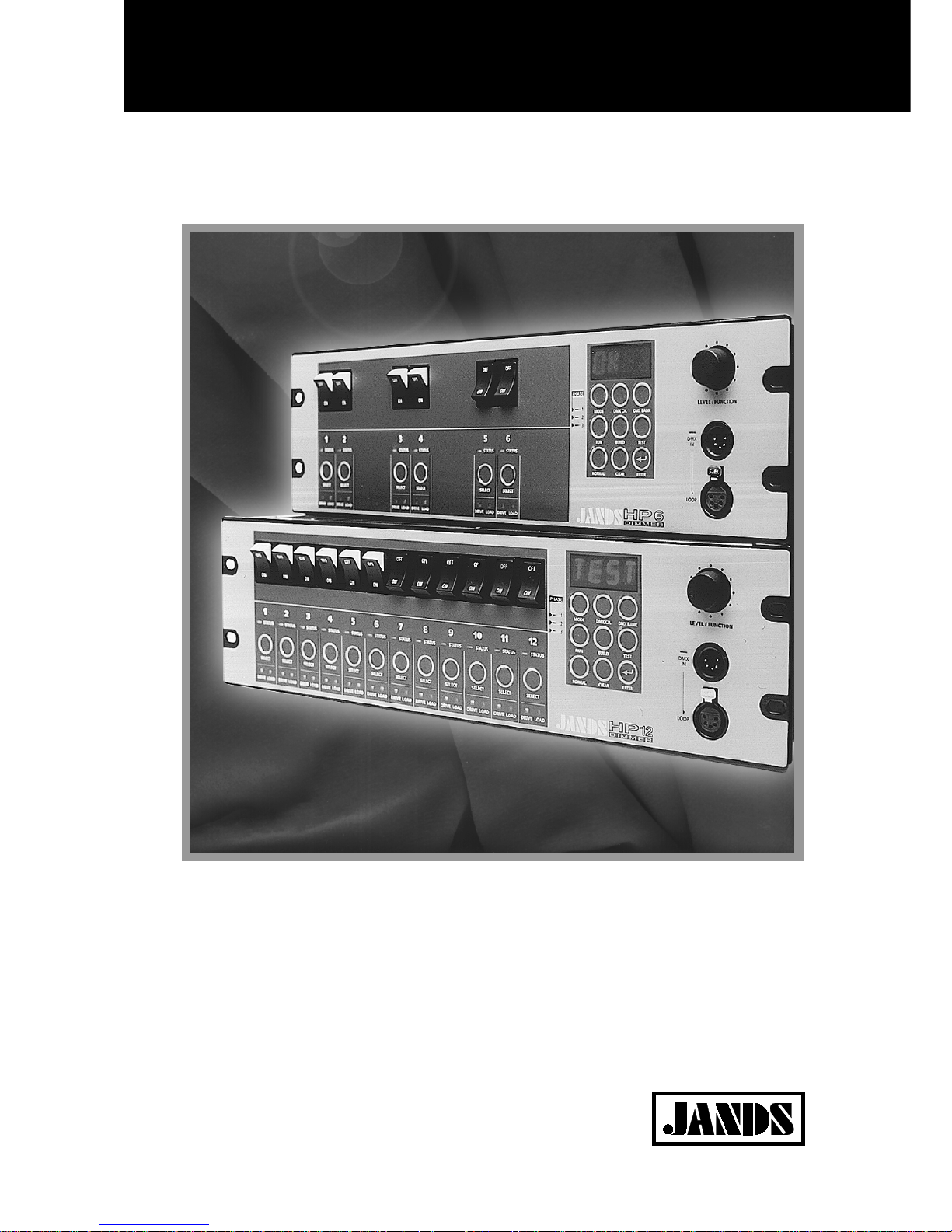
HP6/HP12
Digitally Controlled Dimmer Rack
TTEECCHHNNIICCAALL MMAANNUUAALL
Page 2

Equipment Description ii
Revision 2 - 26 April, 2000 HP SERIES DIMMER TECHNICAL MANUAL
JANDS ELECTRONICS PTY LTD 1997
All rights reserved
DISCLAIMER
Information contained in this manual is subject to change without not ice and does not
re pr es en t a co mmit ment o n t he pa r t o f t he ve ndo r . JAN DS E LE CT RO NI CS P/ L s ha ll
not be liable for any loss or damage whatsoever arising from the use of information or
any error contained in this manual.
It is recommended that all service and repairs on this product be carr ied out by JANDS
ELECTRONICS P/L or it’s authorised service agents.
JAN DS HP S er ies d immer s mus t o nly be use d fo r t he pur po se the y we re in te nde d by
the manufacturer and in conjunction with the operating manual.
JANDS ELECTRONICS P/L cannot accept any liability whatsoever for any loss or
damage caused by service, maintenance or repair by unauthorised personnel, or by use
other t han that intended by the manufacturer.
Manufactured in Australia by:
JANDS ELECTRONICS PTY LTD ACN 001 187 837
40 KENT Rd
Locked Bag 15
MASCOT NSW 2020
AUSTRALIA
PHONE: +61-2-9582-0909
FAX: +61-2-9582-0999
EMAIL: Internet: jandsinfo@jands.com.au
Page 3

Equipment Description iii
Revision 2 - 26 April, 2000 HP SERIES DIMMER TECHNICAL MANUAL
Table of Contents
Table of Contents
1.0 Introduction
1.1 Mains supply wiring............................................................................................1-1
1.2 Phase failure........................................................................................................1-2
1.3 Circuit breakers................................................................................................... 1-2
1.3.1 Overloads and Inrush................................................................................ 1-3
1.3.2 Short Circuits............................................................................................1-3
1.4 Outdoor Systems.................................................................................................1-3
2.0 Equipment Description
2.1 Front panel layout............................................................................................... 2-1
3.0 Circuit Descriptions
3.1 Mains and Low Voltage power supplies.............................................................. 3-1
3.1.1 Mains Circuit Wiring:................................................................................3-1
3.1.2 Mains Radio Frequency Suppression.........................................................3-2
3.1.3 Neutral - Earth Voltage Detection.............................................................3-2
3.1.4 Low Voltage Transformers....................................................................... 3-3
3.1.5 Control Tone Rejection............................................................................. 3-3
3.1.6 Low Voltage DC Supplies........................................................................3-3
3.1.7 Fan Control...............................................................................................3-4
3.2 Phase control...................................................................................................... 3-4
3.3 SCRs and triggering circuits ................................................................................ 3-4
3.4 Output chokes and filtering ................................................................................. 3-6
Page 4

Equipment Description iv
Revision 2 - 26 April, 2000 HP SERIES DIMMER TECHNICAL MANUAL
3.5 Load & drive indicators.......................................................................................3-6
3.5.1 Drive LEDs ..............................................................................................3-6
3.5.2 Load LEDs............................................................................................... 3-6
3.5.3 Load Detecting.........................................................................................3-7
3.6 CPU card............................................................................................................ 3-8
3.6.1 Microprocessor.........................................................................................3-8
3.6.2 Memory.................................................................................................... 3-8
3.6.3 DMX input / output..................................................................................3-9
3.6.4 Zero crossing detector .............................................................................. 3-9
3.6.5 Analog to digital converter (ADC)............................................................3-9
3.6.6 Optocoupler drive..................................................................................... 3-9
3.6.7 5 volt power supply................................................................................ 3-10
3.6.8 Reset generator....................................................................................... 3-10
3.6.9 Rotary encoder ....................................................................................... 3-10
3.7 Front panel card................................................................................................ 3-11
3.7.1 Switches................................................................................................. 3-11
3.7.2 LEDs ...................................................................................................... 3-11
3.7.3 Encoder.................................................................................................. 3-11
4.0 Dimmer Operation
4.1 Menu structure....................................................................................................4-1
4.1.1 ENTER .................................................................................................... 4-1
4.1.2 NORMAL ................................................................................................ 4-1
4.1.3 CLEAR .................................................................................................... 4-1
4.1.4 MODE menu ............................................................................................ 4-1
4.1.5 DMX CHannel menu ................................................................................ 4-9
4.1.6 DMX BANK menu................................................................................... 4-9
Page 5

Equipment Description v
Revision 2 - 26 April, 2000 HP SERIES DIMMER TECHNICAL MANUAL
4.1.7 BUILD menu.......................................................................................... 4-10
4.1.8 RUN menu.............................................................................................. 4-11
4.1.9 TEST function........................................................................................ 4-14
4.2 Deep clear......................................................................................................... 4-14
4.2.1 Quick deep clear..................................................................................... 4-14
4.3 Channel disable ................................................................................................. 4-15
4.4 Software update................................................................................................ 4-15
5.0 Fault Diagnosis
5.1 Protection........................................................................................................... 5-1
5.1.1 Output protection ..................................................................................... 5-1
5.1.2 Thermal protection....................................................................................5-1
5.1.3 Supply Power fault protection ................................................................... 5-2
5.2 Output faults....................................................................................................... 5-3
5.3 Operating faults...................................................................................................5-3
5.4 DMX faults.........................................................................................................5-3
5.5 Phase fault indication...........................................................................................5-4
5.6 Cold lamp filaments............................................................................................. 5-4
5.7 Memory failure....................................................................................................5-4
5.7 Fault finding guide .............................................................................................. 5-5
6.0 Disassembly
6.1 CPU card removal...............................................................................................6-1
6.2 Front Panel card removal.....................................................................................6-2
6.3 Triac / SCR replacement ..................................................................................... 6-3
6.4 “Engine Block” removal...................................................................................... 6-4
Page 6

Equipment Description vi
Revision 2 - 26 April, 2000 HP SERIES DIMMER TECHNICAL MANUAL
7.0 Test and Configuration Settings
7.1 CPU self-tests..................................................................................................... 7-1
7.2 Output card testing..............................................................................................7-2
7.3 Phase Compensation........................................................................................... 7-2
7.4 Dimmer Re-calib ration ........................................................................................ 7-3
8.0 Technical Data and Specifications
8.1 Multipin output connector pin-outs ..................................................................... 8-3
8.2 DMX connector pin-outs .................................................................................... 8-5
8.3 DMX bank allocations.........................................................................................8-5
8.4 Mains wiring colour codes...................................................................................8-6
Appendix A History of Modifications
Appendix B Connector Pinouts
Appendix C Spare Parts
Appendix D Circuit Diagrams
Page 7

Equipment Description 1-1
Revision 2 - 26 April, 2000 HP SERIES DIMMER TECHNICAL MANUAL
1.0 Introduction
1.1 Mains supply wiring
THREE PHASE OPERATION ("NORMAL"):
In Australia the HP12-TR / HP12-SC is normally fitted with a flexible supply cable and
32 amp Clipsal plug. The cable has 6mm2 (40 amp) conductors for t he three phases, t he
neutral and the earth.
Th e 3 2 a mp Clip s a l p lug s u its the ma jor ity of 3 phase v e n u e outlets in Au s tr a lia , and w ill
provide sufficient power to run twelve pairs of 1000 watt PAR64 lamps, assumimg
normal duty cycles.
The incoming mains supply must be protected at not more than 50 amps. The d imme r s '
circuit breakers are not rat ed t o co rrect ly clear faults if the supply protect ion is in excess
of this. Mains supplies are generally protect ed at lower cur rents (32 amps or 40 amps at
most Australian venues). It is up to the user to ensure that the dimmer is used in a
manner that do es not exceed the available supply capacity.
In Australia the HP6-C is normally fitted with a flexible supply cable and 50 amp Clipsal
plug. The incoming mains supply must be protected at not more than 63 amps. The
dimme r ’ s c ircu it br e a k e rs are not r ate d t o corre c tly cle a r fau lts if t h e s upply protection is
in excess of this.
The power cable is t erminated wit hin the dimmer at a six-way terminal block and an
earthing stud. The six-way terminal block has three poles for t he three live mains phases
(labelled A1, A2, A3), and three poles for the mains neutral (N1, N2, N3). The three
neutral poles are bridged with a copper link, with the mains neutral connected t o terminal
N2.
If the supply cable is damaged, it must be replaced with a cable available from JANDS or
its service agents.
SINGLE PHASE OPERATION:
The dimmers may be configured for single phase operation where three phase mains
supply is unavailable.
The dimme r sho uld be supplied with three same-phase actives and three neutrals. The
three active lines must each be prot ected at not more t han 50 amps [63 amps: HP6-C].
The three neutral conductors must each be rated at t he same current as the actives. The
ea rt h conductor should be similarly rated.
The bridge between the three neutral terminal poles (N1, N2, N3) must be removed
before the three incoming neutral lines are connected.
Although it is possible to supply the dimmer with one large single phase feed, the
dimmers' br eakers ar e not ra ted to clear fault s if the supply is protected at currents of
over 50 amps [63 amps: HP6-C].
Th e ne u t r al- e a r t h d et e c t io n will ac t if all t h r ee ne u t r a ls h av e mo r e t h an 15 v o lt s to e ar t h ,
or if any one neutral has more than 45 volts to earth.
Page 8

Equipment Description 1-2
Revision 2 - 26 April, 2000 HP SERIES DIMMER TECHNICAL MANUAL
DELTA SUPPLY OPERATION (ILLEGAL IN MOST COUNTRI E S !)
The available venue mains supply in some countries (eg. the Philip p ine s ) is in the fo rm o f
three phases (220 volts between phases) with no neutral connection. The dimmer ma y b e
configured for operation from 220V delta supplies.
The bridge between the three neutral terminal poles (N1, N2, N3) must be removed
before the three incoming active lines are connected.
• The first incoming active is connected to terminals A1 and N3.
• The second incoming active is connected to t er minals A2 and N1.
• The third incoming active is connected to terminals A3 and N2.
Note that this connection is ILLEGA L in Australia , Europe and the U.K..
Note that this connection renders the output sockets' neutral pins LIVE.
Note that a dimmer wired in this fashion will be subjected to CONTINUOUS
OVERVOLTAGE if connected to the 415V wye or star three-phase supply of most
countries.
The three active lines must each be protected at not more than 50 amps [63 amps: HP6C]. The dimmers' breakers are not rated to clear faults if the supply is protected at
currents of over 50 amps [63 amps: HP6-C]. The earth conductor must be similarly
rated.
Th e neut ra l-ea rt h volt ag e de tec to r w ill sens e whe the r t he "c ent re" (av era ge) volt ag e of
the three phases deviates more than 15 volts from earth.
Once again DELTA CONNECTION IS ILLEGAL AND DANGEROUS IN MOST COUNTRIE S !
1.2 Phase failure
If o n e p o w e r ph as e s hould fa il, t he d immer w ill t u r n o ff t h e o u t p u t s a ss o c iat e d w it h t ha t
phase. This function can be disabled by the operator. See section 4.1.4.5.
1.3 Circuit breakers
Th e circuit breakers protect the HP dimmers' o ut put devices a nd the user’s o utput wiring
against overloads and short circuits. The breakers have a "type 32" delay characteristic,
which is s imilar to standard switchboard b rea kers.
The delay characteristics of the circuit breaker are a delicate balance between high speed
(required for adequate semiconductor pr o tect ion) and surge tolerance (to pass t he inrush
current demanded by large incandescent lamps).
Each of the twelve output circuits is protected by a 11.5 amp [25 amp: HP6-C] fastacting magnetic circuit breaker. These breakers are designed to pass the rated current,
but will d is c onne c t t h e outpu t circu it fo r a n y overlo a d c ond itio n (th e la rge r th e ove r load ,
the quicker the disconnection).
NOTE: The dimmer outlet sockets are rated at 10 amps [20 amps: HP6-C]. Avoid
loading the dimmer outputs beyond the socket capa city.
The breakers protect the dimmer’s output devices from short-circuit loads and faulty
wiring loo ms, a nd save on expen sive dimmer repairs. A tr ipped circu it breaker indicates a
load fa ult tha t r equ ires immediate atten tion.
Page 9

Equipment Description 1-3
Revision 2 - 26 April, 2000 HP SERIES DIMMER TECHNICAL MANUAL
1.3.1 Overloads and Inrush
Co ld lamp fila me n ts c onsu me con s id e rably mor e p owe r th a n w a rm filame nts. Th is me a n s
that the first time the lamp is turned on to full, the surge current can be several times
greater than the rated cur r ent for the lamp.
This cold surge current may be enough to trip the output circuit breakers. If this
“nu isa nc e - t r ipp in g” o f t he c ir cu it b r ea k er s is a p r o ble m, t h e fila me nt P r e he at fa c ilit y ma y
be utilised . See section 4.1.4 .5 for inst ructions on e nabling the Preheat fac ility.
Lamp filament resistance is roughly propo rt ional to temperatur e. A filament preheated to
900°K (630°C) has a resistance about three times higher than a filament at room
temperature (300°K, 30°C).
Preheat turns on the selected channels a very small amount (around 1% at 240 volts and
4% at 110 volts) which heats the lamp filaments and increases their electrical resistance.
When the lamp is then turned on full, the surge current is much less and the circuit
br eak er will not trip .
Other advantages of using Preheat are an increase in lamp life (due to the reduction of
thermal shock to the filament s), and a reduct ion of lamp heat up t ime (the lamps will
flas h sligh tly quick er).
1.3.2 Short Circuits
The SCRs and triacs are protected by the circuit breakers during shorts produced by
damaged wiring or blown lamp filament fragments across the filament supports.
The stress on SCRs and triacs during short circuits depends on:
• The operating temperature of the devices prior to application of the short
• The impedances of the mains supply, dimmer cho kes and output cables
• The let-through energy of the circuit breaker when breaking the fault
• The moment during the mains wavefor m when the sho rt is ap plied
Th e t r ia c s in t he H P1 2 - T R w ill s u rv ive o u t p ut s ho r t cir c u it s u nd e r mo s t c o nd it io n s. T he
more rugged SCR pairs in the HP12-SC, aided by higher choke impedance, will sur vive
output short s under extreme conditions (high operating temperatures, high supply fault
curr ent ava ilability, zero cable le ngth from dimmer to short ).
1.4 Outdoor Systems
It is recommended that at outdoor shows where the power is locally generated the
following steps be taken to ensure a trouble-free show:
1. Run the console from an extension cord that is plugged into t he same power
so ur ce as t he dimme rs. If t his is n ot po ssible a DMX iso latin g unit sho uld be
inserted between t he ligh ting console and the dimmers.
2. Disable the neutral detect system. Generators often have poor regulation on
their output power and it is very likely that under certain circumstances this can
cause the neutral detect feature t o trip.
Page 10
SELECTSELECT
TR
1 7
6
2
5
3
4
891110
Figure 2.1
Page 11

Equipment Description 2-1
Revision 2 - 26 April, 2000 HP SERIES DIMMER TECHNICAL MANUAL
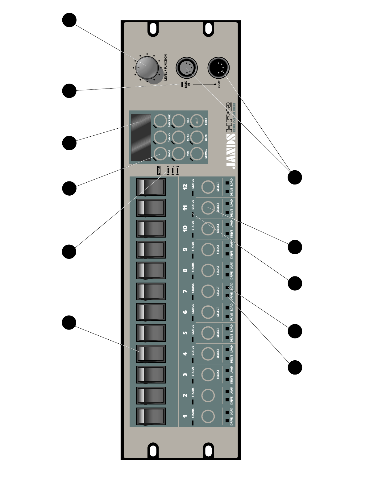
2.0 Equipment Description
2.1 Front panel layout
(
Figure 2.1
1. Channel output circuit breakers: The circuit breakers are rated at 11.5 amps
continuous, however Jands recommend the maximum load connected to a channel be
limit ed t o 1 0 a mps . T he H P6 - C br e ak e r s a r e r a t e d at 25 a mp s b ut J a nd s r ec o mme nd the
maximum channel lo ad be limited to 20 amps. If nuisance tripping occur s, enable the
Preheat option (see section 4.1.4.5). See also section 5.6 for a full explanation of
nuisance tripping.
2. Display: A r ed four dig it alp ha- numer ic dis play is use d to sh ow dimmer st at us a nd
option menus.
3. LEVEL/FUNCTION encoder wheel: This detent action control knob is used to
select items from the menus, and to select the channel levels or chase rat e (depending on
the operat ing mode).
4. DMX IN/LOOP connectors: A standard five pin AXR connector inputs control
desk DMX-512 signals and outputs them to ot her dimme rs via t he Lo o p c o nne ct o r. S ee
section 8.2 for wiring details.
5. DMX IN LED: A green LED indicates the presence of DMX signals.
6. Keypad: These switches are used to select different opt ions and operating modes. A
red LED is associated with each switch to indicate activation of selected function.
7. PHASE LEDs: T hree green LEDs (one for each phase) indicate that the three phase
mains supply is available.
8. Channel SELECT switch: These select or deselect options for each channel, or
switch a chan nel bet ween “on-line ” and “o ff-line”. I f a cha nnel is “off-line”, it will not
respond to the DMX input signals.
9. Channel STATUS LED: A bi-colour LED indicates channel status, ie.
Red = channel set for 110V o utput
Green = channel set for 240V output
Off = channel disabled
Orange = voltage change selected but not yet confirmed
Flashing = channel selected for changes to be made
10. DRIVE LED: This green LED indicates a contr ol signal is being applied to
that channel.
Page 12

Equipment Description 2-2
Revision 2 - 26 April, 2000 HP SERIES DIMMER TECHNICAL MANUAL
11. LOAD LED: This red LED serves two functions. In normal operation, it
acts as an output mimic. When the channel drive is at zero, it indicates whether that
channel’s load is disconnected (or o pen-circuit).
To check a load, set t he channel drive to zero. The LOAD LE D w ill t u r n O N if t he r e is
no lo a d.
For levels above zero, the LOAD L ED w ill mimic the c ha n n e l outpu t wh e never a load is
connected.
Note that the channel circuit breaker must be ON for the LOAD LED circuitry to work.
BREAKER LOAD CHANNEL DRIVE LOAD LED STATUS
on not connected off ON
on connected off OFF
on connected on OUTPUT MIMIC
off doesn’t matter doesn’t matter OFF
Page 13

Equipment Description 2-3
Revision 2 - 26 April, 2000 HP SERIES DIMMER TECHNICAL MANUAL
[ BLANK PA GE ]
Page 14
1 2 3 4 5 6 78
A
B
C
D
8
7654321
D
C
B
A
1
Jands Electronics P/L
40 Kent Rd
Mascot NSW 2020
Australia
Ph (02) 9582-0909
1
5
20-Apr-2000 16:51:13
H:\Lab\HPCE\CIRCUIT\H
p
tr
p
wr4.sch
Title
Size: Number:
Date:File:
Revision:
Sheet of
Time:
A3
Error : F:\PUBLIC\JANDS.EPS image file not suppor
t
MAINS, FAN CONTROL & POWER SUPPLY
HPTRPWR4
OPTO DRIVE CIRCUIT from CPU:
Open-collector switches (ULN2003 ICs) to common.
FRONTPANEL LED CIRCUITS:
Output mimic (load) LEDs are fed by 470R; LED cathodes
connected to common.
Drive LEDs fed by 470R; LED anodes connected to +5 volts.
C18
4n7-Y
C19
4n7-Y
C17
4n7-Y
C16
4n7-Y
C15
4n7-Y
C14
4n7-Y
TR2
Q6040K7
TR1
Q6040K7
R16
10K
RD2
470R
CF2
100nF
OPDIAC2
BRT11
BR2
DB102
RL2
47K
CS2
100nF
RT2
220R
RS2
100R
L2
CB2
11.5A
OPTRAN2
CNY17
OPTRANS13
CNY17
BR16
DB102
RG3
47K
RG2
47K
RG1
47K
D6
D5
D4
D3
D2
D1
C4
100nF
BR13
DB102
BR15
DB102
BR14
DB102
OPTRAN1
CNY17
CB1
11.5A
PTC3
30mA
PTC2
30mA
PTC1
30mA
C3
1uF
C2
1uF
C1
1uF
FAN-A
12V
TEMP1
LM35
C9
2200uF
TX1 TX2 TX3
L1
RS1
100R
RT1
220R
CS1
100nF
RL1
47K
BR1
DB102
R1
15R
R2
15R
R3
15R
C13
33uF
C11
33uF
C12
33uF
GPO1 GPO2
C7
100uF
OPDIAC1
BRT11
CF1
100nF
OTEMP
90DEG
U1B
LM358
Q2
BC557
R5
470R
R6
470R
R7
22K
R8
10K
U1A
LM358
R13
10K
RD1
470R
C8
10uF
TEMP2
LM35
C5
100nF
C6
100nF
R14
470R
R15
470R
Q1
TIP42
R4
1R
TPD
TPN
FL4
FL3
FL2
FL1
TRACKS
FUSIBLE
THREE
240v:14v
PHASE 3 NEUTRAL to CHANNELS 9 - 12
PHASE 2 NEUTRAL to CHANNELS 5 - 8
(STAR or WYE) OPERATION.
LINKED for NORMAL
NEUTRALS 1-2-3
INPUT WIRING OPTIONS
REFER TO MANUAL for
PHASE 1 NEUTRAL to CHANNELS 1 - 4
NEUT1
NEUT3
NEUT2
ACTIVES to BREAKERS
NEUTRALS to OUTLETS
GROUNDS to OUTLETS
CH3 - CH12
LOAD MIMICS
CHANNEL 2 LOAD MIMIC
CHANNEL 1 LOAD MIMIC
OUTPUT MIMIC (LOAD)
10
11
12
1
2
3
4
5
6
7
8
9
+5V to CH3 - CH12
CHANNEL 2 DRIVE
CHANNEL 1 DRIVE
5
42
1
Two channels of twelve shown.
OP2
LO2
LI2
CB2A2K2 G2
1
2
4
5
1
2
4
6
6
4
2
1
5
4
2
1
LEDs
DRIVE/OUTPUT
FRONTPANEL
TO
CARD
CPU
TO
12
11
10
9
8
7
6
5
4
3
2
1
+5
+5
Temp
V-Faults
COM
+Vs
A
B
C
G1K1 A1
NEUTRAL 3
NEUTRAL 2
CB1
PHASE 1
PHASE 2
CHANNEL DRIVE
EARTH
NEUTRAL 1
PHASE 3
1
2
3
4
5
6
7
8
9
10
11
12
CIRCUIT CARD:
HPCEPWR4
HP-12TR TOURING DIMMER
LI1
LO1
OP1
A
E
NA
E
N
4
8
7
6
5
1
2
3
TP+
TP5
TP-
TPT
Ch.1-4
Ch.5-8
Ch.9-12
Page 15
1 2 3 4 5 6 78
A
B
C
D
8
7654321
D
C
B
A
0
Jands Electronics P/L
40 Kent Rd
Mascot NSW 2020
Australia
Ph (02) 9582-0909
027-Apr-2000 13:15:21
H:\Lab\HPCE\CIRCUIT\Hpscpwr6.s01
Title
Size: Number:
Date:File:
Revision:
Sheet of
Time:
A3
Drawn By:
Error : logo2.jpg file not found.
FRONTPANEL LED CIRCUITS:
Output mimic (load) LEDs are fed by 470R; LED cathodes
connected to common.
Drive LEDs fed by 470R; LED
anodes connected to +5 volts.
OPTO DRIVE CIRCUIT from CPU:
Open-collector switches
(ULN2003 ICs) to common.
CON3
Q1
TIP42
C19
4n7-Y
C18
4n7-Y
C17
4n7-Y
C16
4n7-Y
C15
4n7-Y
C14
4n7-Y
CHASSIS
CHASSIS
CON3
CON3
CON3
CON3
R15 470R
R14 470R
C6
100nF
C5
100nF
TEMP2
LM35
C8
10uF
R13
10K
U1B
R8
10K
R7(A-C)
3x10K
R6
470R
R5(A-D)
4x2K2
Q2
BCX17
U1A
CON3CON3
FAN-B
12V
OTEMP
110DEG
C7
100uF
GPO2GPO1
C12A,B
2x33uF
C11A,B
2x33uF
C13A,B
2x33uF
R3
4R7
R2
4R7
R1
4R7
TX3TX2TX1
C92200uF
TEMP1
LM35
FAN-A
12V
CON3CON3
C1
1uF
C2
1uF
C3
1uF
PTC1
30mA
PTC2
30mA
PTC3
30mA
CB1
11.5A
C4
100nF
D1
D2
D3
D4
D5
D6
RG1
100K
RG2
100K
RG3
100K
OPTRANS13
CNY17
CB2
11.5A
CON3
CON3
CON3
CON3
R16
4K7
CON1CON1 CON1CON1
L1 L2
CON1CON1CON1CON1
D8
D9
D10
D11
C202200uF
D12D13
D14D15
D16
D17 D18
D19D20
D21
D22
D23
C21
2200uF
C22
100uF
LP1
220uH
D24
HER303
R18
470R
R19
1K
ARROW
ARROW
R4
1R
CON3
R17
2K2
R20
10K
R21
470R
R22
470R
C10
2n2
TPD
U2
LM2575-5
FUSIBLE
TRACKS
FL1
FL2
FL3
FL4
EARTH BAR
TPT
TP-
TP5
TP+
3
2
1
5
6
7
8
4
N
E
AN
E
A
TOURING DIMMERHP12-SC
FAN CONTROLMAINS WIRING, and POWER SUPPLY
6.0
HPSCPWR6
12
11
10
9
8
7
6
5
4
3
2
1
PHASE 3
NEUTRAL
EARTH
CHANNEL DRIVE
PHASE 2
PHASE 1
D.FORD
NEUTRAL
NEUTRAL
3
4
567
8
9
101112
1
2
3
C
B
A
+Vs
COM
Temp
+5
+5
1
2
3
4
5
6
7
8
9
10
11
12
TO
CPU
CARD
TO
FRONTPANEL
DRIVE/OUTPUT
LEDs
Two channels oftwelve shown.
1
24
5
CHANNEL 1 DRIVE
CHANNEL 2 DRIVE
+5V to CH3 - CH12
9
8
7
6
5
4
3
2
1
12
11
10
OUTPUT MIMIC (LOAD)
CHANNEL 1 LOAD MIMIC
CHANNEL 2 LOAD MIMIC
GROUNDS to OUTLETS
NEUTRALS to OUTLETS
ACTIVES to BREAKERS
NEUT2
NEUT3
NEUT1
PHASE 1 NEUTRAL to CHANNELS 1 - 4
REFER TO MANUAL for
INPUT WIRING OPTIONS
NEUTRALS 1-2-3 LINKED for
NORMAL (STAR or WYE) OPERATION.
PHASE 2 NEUTRAL to CHANNELS 5 - 8
PHASE 3 NEUTRAL to CHANNELS 9 - 12
240:14V
THREE
NN
OP1
LO1
LI1
CB1
OP2
LO2
LI2
CB2
MIMIC1
DRIVE1
+5V
COMMON
+10V
+10V
COMMON
+5V
DRIVE2
MIMIC2
+7.6V to CH3-CH12
COMMON to CH3-CH12
MAINS VOLTAGES
LOW VOLTAGES
THYRISTOR CONTROL CIRCUITS:
REFER TO DIAGRAM HPSCHDF4
Refer to diagramHPSCHDF5
for thyristor firing circuits.
TPN
3
4
567
8
9
101112
3
4
567
8
9
101112
+Vs
+7.6V
Neutral
Detect
Page 16

1 2 34
A
B
C
D
4
321
D
C
B
A
Title
Number RevisionSize
A4
Date: 20-Apr-2000 Sheet of
File: D:\R_&_D\HPDIMMER\CIRCUIT\Hpschdf3.s01Drawn By:
ARROWARROW
ARROW
ARROW
ARROW
ARROW
ARROW
ARROW
OPTRAN1
CNY17
DP1
DN1 DM1
DL1
RL1
47K
RS1
100R
CS1
47nF
CF1
47nF
SCRB1
SCRA1
L1
CON1
CON1
CON1
CON1
RY1
2R7
RX1
68R
RW1
68R
RP1
10K
RA1
10K
RB1
4K7
RC1
2K2
QA1
BCX19
QB1
BCX19
QC1
BCX19
QE1
BCX19
QG1
BCX19
QD1
BCX17
QH1
BCX17
CA1
100uF
CB1
1uF
TX1
DA1
DB1
DC1
DD1
DE1
DF1
DG1
DH1
DJ1
DK1
RD1
100K
RE1
100K
RF1
100K
RH1
4K7
RJ1
4K7
CC1
2n2
RK1
4K7
RM1
4K7
RN1
4K7
RQ1
2K2
RR1
4K7
ARROW
CD1
100nF
CE1
100nF
RU1
68R
RV1
68R
3
D.FORD
HPSCHDF3
LOW VOLTAGES MAINS VOLTAGES
LEDs
MIMIC
LOAD
to
SUPPLY
+5V
SUPPLY
+10V
NEUTRAL
MAINS
LOAD
to
OUTPUT
BREAKER
POWER
MAINS
from
NEUT1 OP1 LO1 LI1 CB1
HP12-SC SCR FIRING & OUTPUT
CHANNEL 1 SHOWN
from
ULN2003
on CPU
CARD
One of twelve circuits per unit shown.
This diagram is a part of diagram
2W
3W
Q6035K
Q6035K
All diodes BAV103.
All resistors 1/16W
SMT unless stated.
HPSCPWR3.
Page 17

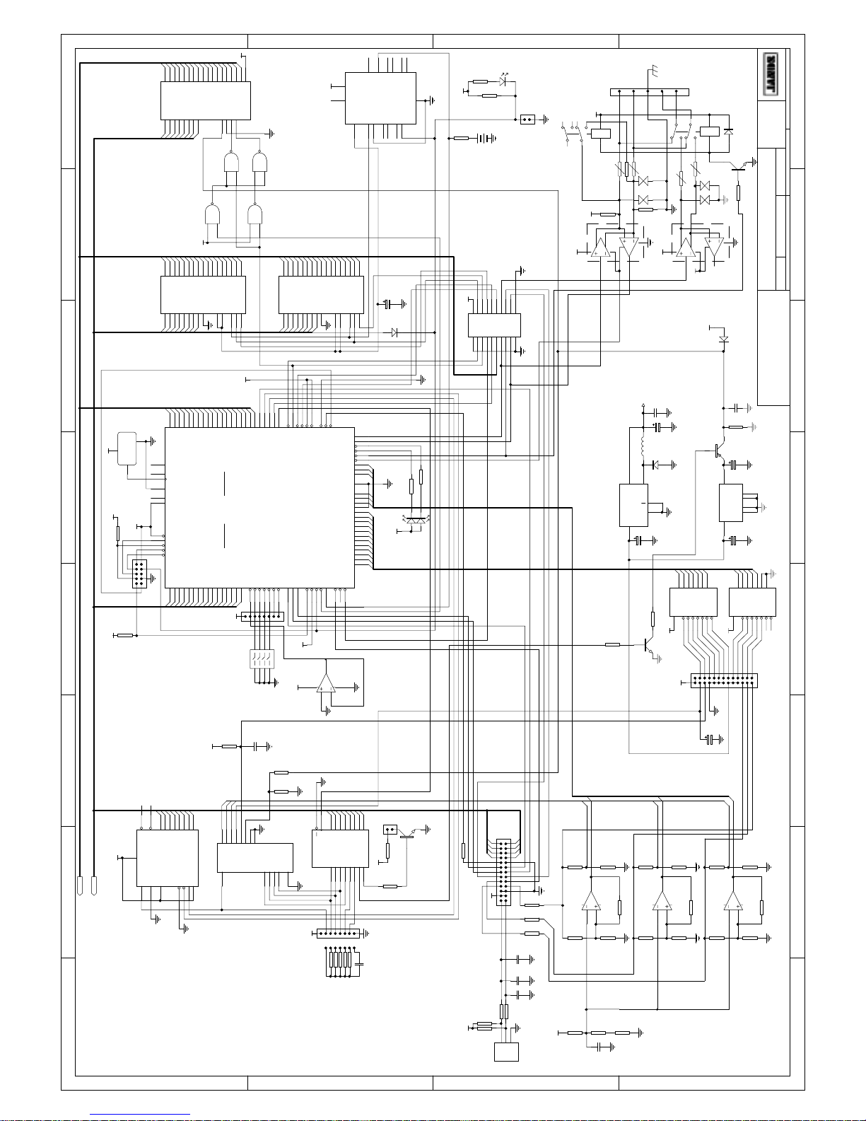
Equipment Description 3-1
Revision 2 - 26 April, 2000 HP SERIES DIMMER TECHNICAL MANUAL
3.0 Circuit Descriptions
(
Figure 3.1
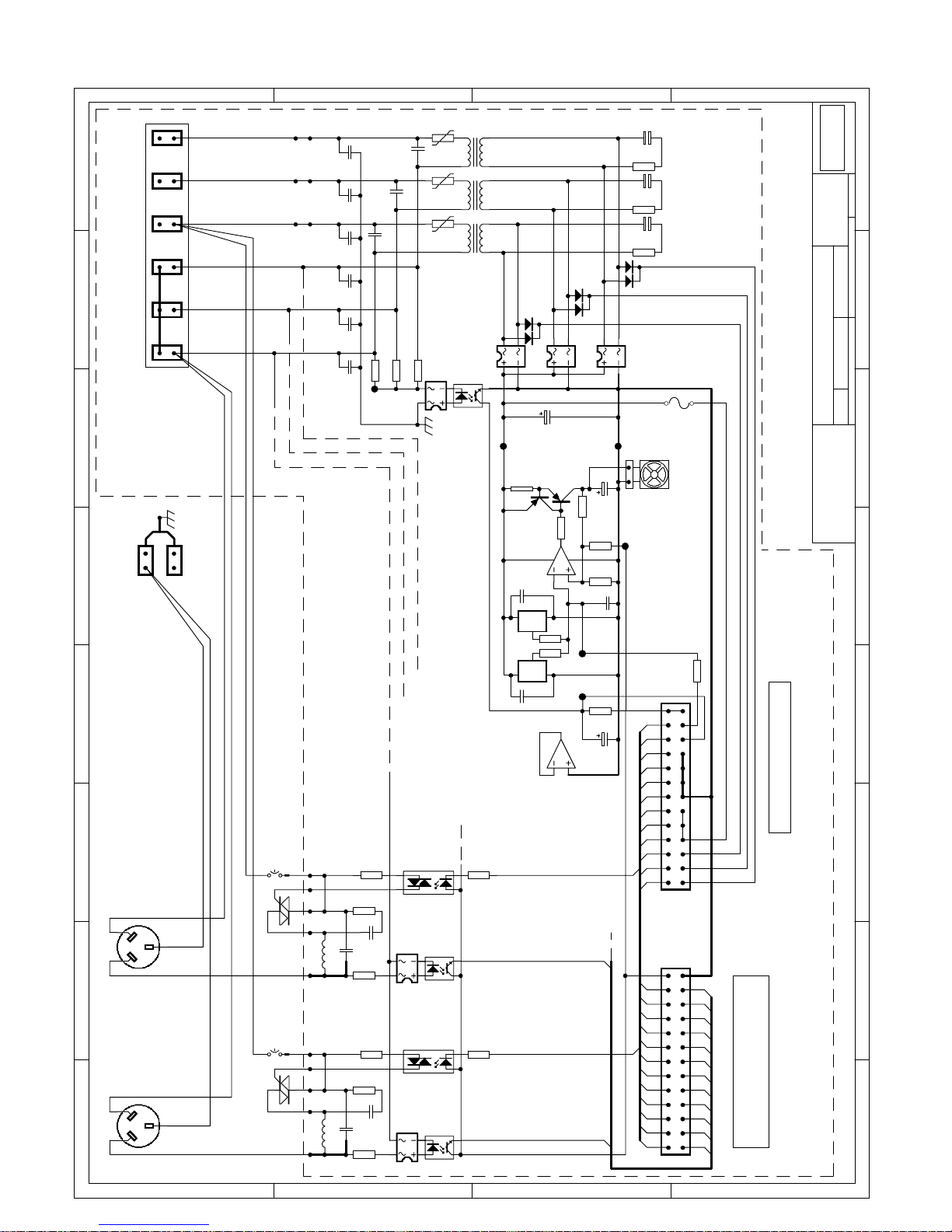
The Output PCB contains the circuitry for the output devices (triacs in the HP12-TR and
SCRs in the HP12-SC and HP6-C), the temperature-controlled fan, and the 15 volt
power supply.
3.1 Mains and Low Voltage power supplies
Th e d imme r ele c t r o nic s us e s lo w volt a ge d c p o w e r at 15 volt s (u n re g u lated ) a nd 5 v o lt s
(regulated). The HP12-SC also uses a 10V regulated supply for the gate drive
os cillators. The unregu la ted DC p owe r is s upplied by three transformers mounted on the
output PCB.
3.1.1 Mains Circuit Wiring:
The mains circuits of the HP dimmers are co nfigur ed as three separate phase circuits,
with four channels per circuit. The three active mains inputs and three separat e mains
neutral inputs appear at a terminal block, labelled A1, A2, A3 and N1, N2, N3
respectively. The ground ter minal is an adjacent M4 stud.
This wiring allows the dimmer to be configured for three-phase star (wye) mains
supplies, three-phase delta supplies or single-phase supplies.
THREE PHASE OPERATION ("NORMAL"):
Th e r ac k mo u nt HP dimme rs ar e no rma lly supplied with a three-phase power cable and
plug attached, suiting the vast majority of available mains supplies (ie. three phase and
neutral). The three live mains phases are connected to terminals A1, A2, A3. The three
neutral poles are bridged with a copper link, with the mains neutral connected t o terminal
A2.
SINGLE PHASE OPERATION:
The dimmers may be configured for single phase operation where three phase mains
supply is unavailable.
The dimme r sho uld be supplied with three same-phase actives and three neutrals. The
three active lines must each be prot ected at not more t han 50 amps [63 amps: HP6-C].
The three neutral conductors must each be rated at t he same current as the actives. The
ea rt h conductor should be similarly rated.
The bridge between the three neutral terminal poles (N1, N2, N3) must be removed
before the three incoming neutral lines are connected to these terminals. The three
incoming actives are connected t o A1, A2, A3.
Page 18

Equipment Description 3-2
Revision 2 - 26 April, 2000 HP SERIES DIMMER TECHNICAL MANUAL
DELTA SUPPLY OPERATION (ILLEGAL IN MOST COUNTRI E S !)
The available venue mains supply in some countries (eg. the Phillip in es ) is in t he fo r m o f
three phases (220 volts between phases) with no neutral connection. The dimmer ma y b e
configured for operation from 220V delta supplies.
The bridge between the three neutral terminal poles (N1, N2, N3) must be removed
before the three incoming active lines are connected.
• The first incoming active is connected to terminals A1 and N3.
• The second incoming active is connected to t er minals A2 and N1.
• The third incoming active is connected to terminals A3 and N2.
Note that this connection is ILLEGAL in Australia, Europe and the U.K. since this
connection renders the out put sockets' neutral pins LIVE.
No te t hat a dimme r wire d in this fas hion w ill be sub jected t o CONT INUOUS OVERVOLTAGE if connected to the 415V wye or star three-phase supply of most countries.
3.1.2 Mains Radio Frequency Suppression
Radio-frequency interference generated by phase-controlled dimming is heavily
attenuat ed before it can contaminate the mains supply.
Capacitors C1, C2 and C3 (1uF 275VAC X2 rated) are connected from each incoming
active (A1, A2, A3) to the corresponding neutral (N1, N2, N3).
Capacitors C14 thru C19 (4700pF 275VAC Y2 rated) are co nnected from each incoming
active and neutral to ground.
The mains circuits are protected from (improbable) catastrophic failure of these
capacitors by fusible PCB track links (labelled FL1 thru FL4). Failure of these links will
remove power from the low-voltage transformer associated with that phase. The links
may be re new ed du ring rep airs by wir e links (a s ingle s tr and o f flexib le wir e, n ot mor e
than 0.2mm dia).
3.1.3 Neutral - Earth Voltage Detection
Voltages of more than 15V (AC average) between neutral and earth are a strong
indicator of mains supply problems (eg missing or weak neutral connection, or missing
earth).
Th e vo ltage from the dimmer s' ea rt h to each of the three neutrals is sensed by three 100K
resistors (RG1, RG2, RG3), full-wave rectified and fed to the input LED of an
optoisolator.
When the dimmer is configured for normal three-phase star connection, the three
incoming neutrals are bridged, yielding an impedance of 33K from neutral to gro und and
a sensitivity of 15V AC average.
If t h e d imme r is c o nf igu r e d fo r t h r ee s ame - p ha se inp u t s, each neutral has a sensitivity of
45V (or 15V for all three neutrals).
If the d imme r is c onfig u r ed for d e lta ope ratio n (with no incoming neutra l) th e c ircu it will
detect when the "centre average" of the three phases deviates more than 15V from earth.
Page 19

Equipment Description 3-3
Revision 2 - 26 April, 2000 HP SERIES DIMMER TECHNICAL MANUAL
3.1.4 Low Voltage Transformers
HP12-TR: The transformers are nominally rated at 375V (primary), 23V (secondary).
Th e p rima ry w ind ings o f t hes e t r an sfo rme r s w ill to le ra t e 415 vo lts without o verheating.
They are protected against secondary-side overloads by card-mounted 30mA PTC
thermistors. These thermistors are sized NOT to trip during mains overvoltages, but
WIL L tr ip if a lo w vo lta ge fa ult o cc urs . T hermis to r c uto ut will t ur n off the fro ntp anel
PHASE LED.
HP12-SC, HP6-C: The transformers are nominally rated at 240V (primary), 15V
(secondary). The primary windings are protected against secondary-side overloads by
card-mounted 30mA PTC thermistors. These thermistors will trip during continuous
mains overvoltages of more than 340V. Thermistor cutout will turn off the frontpanel
PHASE LED.
If t her mist or c ut ou t o ccu rs, the y may be r ese t by t ur ning off p owe r t o the dimmer for
five seconds. However, since thermistor cutout will never occur during normal
operat ion, t he cause o f cutout should be investigated.
3.1.5 Control Tone Rejection
Control to nes are superimposed on mains voltages by supply authorities to co ntrol offpeak heaters etc. Tone frequencies of 750 Hz and 1050 Hz are common, although
frequencies from 167 Hz to 1750 Hz are in use. Amplitudes are typically less than 5
volts, although higher levels have been reported at some locations.
These tones may cause flicker in dimmed lamps, due to jitter in the detected zerocrossing position.
Th e e ffe c t o f c ontrol t ones is min imis e d b y filter in g a t t h e s e c ondary w in d in g s o f the low
voltage transformers. Resistor-capacitor networks (R1-CF3, R2-CF4, R3-CF5), in
conjunction with inherent transformer inductances, form a 12 dB/oct filter at 400 Hz.
Control tones at levels up to 15 volts at 750 Hz, or 25 volts at 1050 Hz, have little effect
on performance.
3.1.6 Low Voltage DC Supplies
Each of the three tr ansformers has two asso ciated rect ifiers. One set o f rectifiers feeds
the common DC supply filter capacitors, while the other provides full-wave rectified
waveforms to the zero- crossing detect ors and three phase indicator LEDs via the Front
Panel PCB.
Th e dimme rs’ u nre gula ted supply is filtered by C9 (2200uF) and directly feeds the fan
controller, the overvoltage detector and the temperature sensors. All other circuits are
supplied via the OTEMP overtemperature cut out.
Th e dimme r w ill shut d ow n und er so ftw are co nt ro l at 8 5°C. If t he d immer ma nag es t o
reach higher temperatures than this, the OTEMP cutout will remove power from all
cir cu it s e xce p t t h e fa n c o ntroller a nd a ss o cia t e d cir c u it s. T he fa n s pe e d w ill in cr e a se d u e
to lighter supply loading.
The unregulated dc voltage at the common supply filter capacitor (C9) is normally
ar oun d 1 4 ~ 1 5 v olt s b u t may drop a s low a s 1 1 vo lts w ith lo w mains v olta ges , or rise in
excess of 20V during severe mains overvoltages.
Mains overvoltages are sensed as high unregulated DC voltages by op-amp U1b. Since
the DC supply voltage is dependent on dimme r lo a d ing as w ell a s main s v o lt a ge , t h e t r ip
point of this circuit may vary from 260V to 280V AC mains voltage.
Page 20

Equipment Description 3-4
Revision 2 - 26 April, 2000 HP SERIES DIMMER TECHNICAL MANUAL
3.1.7 Fan Control
Temperatures are sensed by LM35DZ sensors mounted at the exhaust ("hot") ends of the
heatsinks. These sensors have an output voltage of 10mV per degree Celsius (ie. 300mV
at 30°C). Their output voltage is summed and fed to the frontpanel CPU card for
temperature display, and to the 12 volt dc fan control.
The fan speed controller is a DC amplifier formed by op-amp U1a and transistor Q1. The
fan is "held off" until sensor temperatures reach 30°C by resistor R16 from the 5V rail.
The fan voltage reaches 12V at t emperatur es of 50°C.
The circuit is protected against shorts in the fan or its wires by transistor Q2, which
clamps the out put current at 0.6 amps.
3.2 Phase control
Th e p ow er a pp lied t o a lo ad is va r ied by co nt r o lling t h e p oin t o f t hyr ist o r firin g in each
mains half-cycle.
The convention used here is that firing angles of 0° (0 radians) occurs at t he end of each
half cycle, and give zero output. Firing angles of 180° (π radians) occurs at the beginning
of each half cycle, giving maximum (unity) output.
The traditional method of achieving phase control (ie. firing position control) has been to
generate a "ramp" voltage in each half-cycle, which is then compared t o t he dc contro l
signal.
Key elements in this technique are:
• The ramp begins just after the st art of the half cycle, at a voltage equal to the
maximum control voltage.
• The ramp ends just before the finish of the half cycle, at a voltage equal to the
minimum control v oltage.
• The beginning and end of the ramp are determined by zero crossings of the
mains wav eform.
• The shape of the ramp determines the control law (CV to P law).
No t e t h at the finit e wid t h o f t he z er o - c r o s sing p u lse c au s es t he d immer t o jump fr om no
firing to some small firing angle as soon as contro l voltage is applied. The snap-on firing
angle is defined by the zero cro ssing pulse width.
This is actually a ver y mino r pr oblem since zero c rossing puls es o f 2.2 ms (±1100 µs
around tr ue zero crossing) give a snap-on power o f less than 1%. The HP has a zerocrossing pulse width less than 2 ms.
The HP micropro cessor (µP) generat es its "ramp" digitally, and specifically shapes the
ramp to pro vide linear control-to-power characteristics. The µP then compares the DMX
channel information with the generated ramp information and turns on the appro priate
output device at the required point on each mains half-cycle.
3.3 SCRs and triggering circuits
HP12-TR:
The triacs used in the HP12-TR are 40 amp, 600 volt devices (type Q6040K) with 2500
volt isolation to t he mounting tab. They have a surge current rat ing of 335 amps for 10
millise cond s. The d immer w ill func tio n wit h re placement triacs of lower ratings but its
ability to s urv ive shor t circuits and ove rvoltages will be jeopardised.
Page 21

Equipment Description 3-5
Revision 2 - 26 April, 2000 HP SERIES DIMMER TECHNICAL MANUAL
The output devices are triggered with Siemens BRT12 opto-isolators. These are
optically triggered SCRs rated at 600 volts.
Opto-triggered dimmers have a lower ability to correctly drive low-power inductive
loads than DC-fired SCR dimmers. Although this is true of the HP12-TR, careful
snu bber des ign and comp one nt se lect ion guar ant ees tha t it will co rr ect ly dr ive a ll load s
from rated maximum down to 25 watt transformer pinspots.
When the lamp blows in a transformer-driven pinspot, the unloaded t ransformer primary
pr es ent s a ve ry s mall, hig hly ind uc t ive lo a d. T he H P1 2 -T R d immer may mis be hav e w ith
such a lo ad. However, if two o r mor e pins pot s are connec ted to a dimmer channel, a
lamp failure in one pinspot will have n o adverse effects.
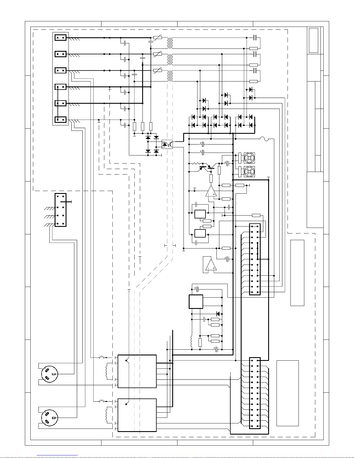
HP12-SC/HP6-C:
The SCRs used in the HP12-SC are 35 amp, 600 volt devices (type S6035K) with 2500
volt isolation to t he mounting tab. They have a surge current rat ing of 425 amps for 10
millise cond s. The d immer w ill func tio n wit h rep lacement SCRs of lower rat ings but its
ability to s urv ive shor t circuits and ove rvoltages will be jeopardised.
The SCRs used in the HP6-C are 65 amp, 600 volt devices (type S6065) with 2500 volt
isolation to the mounting tab. They have a surge current rating of 800 amps for 10
millise cond s. The d immer w ill func tio n wit h rep lacement SCRs of lower rat ings but its
ability to s urv ive shor t circuits and ove rvoltages will be jeopardised.
The SCRs are connected in back-to-back pairs, such that during each mains half-cycle
one SCR is b locking (re verse biased) and the oth er will co nduct if trigge red.
HP12-SC: The SCR gates are triggered with continuous DC (as opposed to trains of
pulses), which forces the SCRs to conduct even if the load current is lower than the SCR
latchin g curr ent. This a llows exc ellent control over small an d highly inductive load s.
The DC gate firing current for the twelve SCR pairs is provided by twelve power
os cilla to rs . T he 40kHz po wer oscillat or s o pe rat e fr o m a 1 0V reg ula te d supply, and are
contro lled by phase-control signals from the CPU.
The oscillator outputs drive pulse transformers. The two secondary (mains-side)
windings of the pulse transformers are full-wave rectified and fed to the SCR gates.
Sufficient gate current is generated to correctly trigger the SCRs at very low
temperatures (minus 10°C).
Ea ch o f the tw elve osc illat or s is pro t ec te d by a 2R7 supply resistor, such that failure in
an o s cilla t o r fu se s t he r es isto r witho u t d isr u p t ing o t h er o s c illat or s. E a ch o sc illa t o r d ra w s
8mA when inactive, and around 80mA when that channel is driven to full.
HP6-C: The SCR gates are triggered with Siemens BRT12 opto-isolators. These are
optically triggered SCRs rated at 600 volts.
Op to - tr ig g e red S C R dimme rs ha ve a low e r ab ility to correc tly drive low-powe r in d u ctiv e
loa ds tha n DC -fir ed SCR dimme rs. Alt ho ugh th is is t ru e o f t he H P6- C, ca refu l snu bbe r
design and compon ent sele ction g uarantee s th at it will correctly drive a ll loads fr om rated
maximum down to 40 watt pinspot tr ansformers.
When the lamp blows in a transformer-driven pinspot, the unloaded t ransformer primary
presents a very small, highly induct ive load. The HP6-C dimmer may misbehave with
such a lo ad. However, if two o r mor e pins pot s are connec ted to a dimmer channel, a
lamp failure in one pinspot will have n o adverse effects.
Page 22

Equipment Description 3-6
Revision 2 - 26 April, 2000 HP SERIES DIMMER TECHNICAL MANUAL
3.4 Output chokes and filtering
Th e chokes and filters minimise the emission of high frequen cy interference radiated from
dimme r outpu t wires. Th e fa s t ris ing wa ve forms produ c e d b y p h a s e - c ont ro lle d tria c s a nd
SCRs have large amounts of high frequency energy, which would be radiated as
electromagnetic interference (EMI) without the chokes.
The degree of suppression at low frequencies (150Hz - 150kHz) is indicated by the
output voltage risetime. Longer risetimes indicate superior suppression, lower acoustic
noise in lamp fila ment s and less "buzz" co upled into audio wiring.
The HP12-SC chokes have a risetime of over 500 microseconds, measured from 10% to
90% of the rising waveform edge, when driving a 2500 watt incandescent load at 90°
firing angle. The HP12-TR chokes have a risetime of 280 microseconds when measured
in the same fa shion.
The suppression at frequencies above 150kHz must meet Australian and international
standards; the HP6-C, HP12-TR and HP12-SC provide suppression superior to statut o ry
requirements.
High frequency output filtering in the dimmers is provided by capacitors (CF1 thru
CF12) connected from the SCR/triac hot input to t he choke out put. I n addition, snubber
components RS1 thru RS12 and CS1 thru CS12 serve to reduce the amplitude of
commutation transients.
NOTES: HP12-TR / HP12-SC / HP6-C
Dimme r cha nnels not dr iven o n will " leak " 50 Hz AC cur ren t t hro ugh the RF-f ilter and
snubber capacitors to their loads. The HP12-TR uses 100nF snubber and filter
ca p a c ito rs, an d w ill pass u p to 15mA to the load; t h e H P 12- SC u s e s 4 7 n F c a p a citor s a nd
will p as s up t o 7mA . T he HP 6 - C u s es 100nF snubber and filter capacitors, and will pa ss
up to 22mA to the load.
Th is c a p a c ito r c urr ent w ill h a ve n o sig nific ant e ffe c t o n load s g r eat er t h a n 20 [40 ] wa tt s ,
but may c aus e a g low (simila r to p rehe a ting ) in ve r y s ma ll pilot lamps o r slo w rot a tio n in
sma ll mo t o r s an d fa ns . S mall d imma ble flu o r es c en t a nd ne o n la mp s may no t d im t o z er o
due to this leakage.
Pr oblems cause d by capac itor cu rre nt may be lar gely e liminate d by co nnec ting a s mall
resistive or incan des cent lo ad in parallel with the des ired load.
3.5 Load & drive indicators
3.5.1 Drive LEDs
Each channel's Drive LED is connected to t he same phase-contr ol signals (generated by
the CPU) which trigger the HP12-TR's / HP6-C's opto-isolators or the HP12-SC's power
os cillat ors . The Dr ive LE D mimics t he p hase-co ntr ol drive to the tr iacs o r SC R pa irs.
The LED intensity is linearly contro lled by the duty cycle of the drive, but visually does
not appear t o be linear.
3.5.2 Load LEDs
Ea c h c h a nn e l’ s L oad L E D is c onne c ted a s a n outpu t volt a g e mimic. T he Load L E D s a re
op to -is olat ed fro m th e dimme r ou tp ut s. T he o pto -is olat o rs ar e d riven from t he o ut put s
via a 47K resistor and bridge rectifier. The "neutral retur n" from each channels' bridge
rectifier ret ur ns t o the neutral associated with that channels' phase (N1, N2 or N3).
Page 23

Equipment Description 3-7
Revision 2 - 26 April, 2000 HP SERIES DIMMER TECHNICAL MANUAL
The opto -isolators' output drives the Load LEDs via 470R resistors from the 5 vo lt rail
at up to 6mA. Although the LED current is vaguely proportional to output voltage,
visually it is not linear due to L ED and percep tual non-lin ear ities.
3.5.3 Load Detecting
Whe n no loa d is c on nec te d, the Lo ad LED will lig ht . T he snu bber a nd filt er c apa cit or s
(100nF for HP12-TR and HP6-C, 47nF for HP12-SC) will p as s a n ac c ur r e nt of 7mA t o
22mA, which is sensed by the Load LED as an output voltage.
The Load LED may be used to indicate the presence of a load only when no drive is
present, and the channel’s breaker is on. In this case, NO LOAD = LED ON;
CHANNEL LOADED = LED OFF.
When the channel is driven (as indicated by the Drive LED) the Load LED will act
simp ly as an output mimic.
Page 24
1 2 3 4 5 6 7 8
A
B
C
D
87654321
D
C
B
A
1
Jands Electronics P/L
40 Kent Rd
Mascot NSW 2020
Australia
Ph (02) 9582-0909
127-Apr-2000 11:57:37
H:\Lab\HPCE\CIRCUIT\Dimc
p
u8.sch
Title
Size: Number:
Date:File:
Revision:
Sheet of
Time:
A2
Drawn By:
CIRCUIT COMMENTS
- The DMX-512 input can be used in loop back or party line mode.
- Mains fluctuations can be compensated.
- FLASH ROM program storage.
CE1
1nF
RE5
4k7
RE4
10k
RE3
18k
RE2
39k
RE1
82k
R45
10k
Q4
BCX19
R44
10k
R42
100k
R43
100k
Q3
BCX19
1
2
3
IC15A
74HC00
C5-10,C12-14
100nF
+5
C1
10nF
C2
10nF
COM
9
1B
1
1C
16
2B
2
2C
15
3B
3
3C
14
4B
4
4C
13
5B
5
5C
12
6B
6
6C
11
7B
7
7C
10
IC9
ULN2003
R36
100R
+5
+5
C15
100nF
R12
10k
R27
4K7
+5
3
2
1
411
IC14A
LM324
+5
R38
2k2
A012A111A210A39A48A57A66A75A827A9
26
A1023A1125A124A1328A1429A15
3
CE22OE
24
D013D114D215D317D418D519D620D7
21
A162A17
30
VPP
1
IC10
27020
+5
R2
1K
R1
1K
R4
10k
R3
10k
+5
C17
10uF
+5
R26
1k
LED3
RESET
R18
22k
R16
1M
+5
RLY1
MR62
RLY2
MR62
R5
100R
+5
+5
R17
10k
10
9
8
IC14C
LM324
D0
111
A1
20
D1
110
A2
21
D2
109
A3
22
D3
108
A4
23
D4
105
A5
24
D5
104
A6
25
D6
103
A7
26
D7
102
A8
27
D8
100
A9
30
D9
99
A10
31
D10
98
A11
32
D11
97
A12
33
D12
94
A13
35
D13
93
A14
35
D14
92
A15
37
D15
91
A1638A1741A1842A19
121
A20
122
A21
123
A22
124
A23
125AS82
R/W79SIZ081SIZ1
80
BERR
70
DSACK0
89
HALT69RESET68BR
113BG114
XTAL
60
BGACK
115
IRQ177IRQ276IRQ375IRQ474IRQ573IRQ672IRQ7
71
A0
90
TP0
16
TP1
16
TP2
14
TP3
13
TP4
12
TP5
11
TP6
10
TP7
9
TP8
6
TP9
5
TP10
4
TP11
3
TP12
132
TP13
131
TP14
130
TP15
129
T2CLK
128
FC2
120
FC1
119
FC0
118
DSACK1
88
CSBOOT
112
AVEC
87
RMC
86DS85
MODCLK
78
IFETCH
55
IPIPE
54
BKPT
56
FREEZE
58
TSTME
57
EXTAL
62
XFC
64
CLKOUT
66
VDDSYN
61
MISO
43
MOSI
44
SCK
45
PCSO
46
PCS1
47
PCS2
48
PCS3
49
TXD
52
RXD
53
VSTBY
19
IC1
68332
+5
Vcc
20
Vin
1
INT
9
Vrf(-)
11
OFL
18
Vrf(+)
12
DB02DB13DB24DB3
5
CS
13
DB4
14
RD
8
DB5
15
WR/RDY
6
DB6
16
MODE
7
DB7
17
IC4
ADC0820
X013X114X215X312X41X55X62X7
4
INH6A11B10C9VEE
7
X
3
IC6
4051
+5
BATT
CR2032
+5
123
45
678
SW1
LED1
Red
LED2
Green
R24
1k
R23
1k
+5
OC
1
CLK
111D22D33D44D55D66D77D88D9
1Q192Q183Q174Q165Q156Q147Q138Q
12
IC5
74HC574
R25
1k
R37
1k
Q1
BCX19
+5
+5
CEO12CEI13VOUT
2
VCC
3
VBATT
1
RES16WDI
11
GND
4
OSC17OSC2
8
LOW
6
PFI
9
PFO
10
BAT-ON
5
/RES
15
WDO
14
IC8
MAX691
+5
R10
10k
+5
+5
A012A111A210A39A48A57A66A75A827A9
26
A1023A1125A124A1328A143A15
31
CE22OE
24
D013D114D215D317D418D519D620D7
21
A16
2
WE29CS30VCC
32
IC2
62010
A012A111A210A39A48A57A66A75A827A9
26
A1023A1125A124A1328A143A15
31
CE22OE
24
D013D114D215D317D418D519D620D7
21
A16
2
WE29CS30VCC
32
IC3
62010
R9
10k
R30
22k
R33
4k7
+5
C18
10uF
D1
HER303
L1
220mH
C3
220uF
C4
220uF
R11
10k
+5
D2
BAV21
R39
100k
+5
C11
100nF
+5
R40
2k2
R41
2k2
+5
4
5
6
IC15B
74HC00
8
9
10
IC15C
74HC00
11
12
13
IC15D
74HC00
Vin
8
GND
2
GND
3
GND
6
GND
7
Vout
1
REG2
MC78L12CG
C22
10uF
C21
10uF
Q2
BCX17
R6
1k
R8
1k
C20
100nF
D3
BAV21
+5
IC11
75176
IC12
75176
IC7
GAL16V8
+5
D4
SM4936
+5
8
(For test only)
External DAC
16,19,23,25,27
5
4
6
1
8
5
6
7
A
B
C
DXO
SZ1
SZ0
LWR
HWR
RRD
HCLCnc
RXD
CON
TXDA0RAM
COLRWAS
nc
Mux Expansion
100k
RN1
Zero cross gens
Encoder
RST
3
4(-)
5(+)
2(-)
Input
Output
DMX
1(+)
1265.82/B2
HP6/12 Dimmer CPU
Drive to Optos
BDM
CN1
Spkr
+5
Temp
gnd
Unreg
HSinA
HSinB
HSinC
Ch1
Ch2
Ch3
Ch4
Ch5
Ch6
Ch7
Ch8
Ch9
Ch10
Ch11
Ch12
Power Supply
To Power PCB
D0
C
B
A
ABC
Sns
(View from solder side)
TO FRONT PANEL CARD
WE
31
Flash Control
/28F020
4
8
231
3
2
R19
22k
R13
1M
R20
10k
12
13
14
IC14D
LM324
R29
22k
R32
4k7
R22
22k
R15
1M
R21
10k
5
6
7
IC14B
LM324
R28
22k
R31
4k7
COM
9
1B
1
1C
16
2B
2
2C
15
3B
3
3C
14
4B
4
4C
13
5B
5
5C
12
6B
6
6C
11
7B
7
7C
10
IC13
ULN2003
C24
10nF
+5
+5
R48
1k
R46
22k
R47
10k
Vin
1
Vout
2
GND
3
FB
4
ON
5
REG1
LM7526-5
+5
7
TH1
C870
TH2
C870
MOV1
1.5KE
MOV2
1.5KE
TH3
C870
TH4
C870
MOV3
1.5KE
MOV4
1.5KE
D(0..15)
A(0..18)
29-32
R7
2K2
123456789
10 11
121314151617181920
GND
2
Vcc
4
OUT
3
OSC1
16MHz
CONN5
1
1
CONN4
1
15
CONN1
C
B
A
D8D9D10
D11
D12
D13
D14
D15
D8D9D10
D11
D12
D13
D14
D15
D8
D9D10
D11D12
D13D14
D15
D0D1D2D3D4D5D6
D7
D8D9D10
D11
D12
D13
D14
D15
D8D9D10
D11
D12
D13
D14
D15
A0A1A2A3A4A5A6A7A8A9A10
A11
A12
A13
A14
A15
A16
A1A2A3A4A5A6A7A8A9
A10
A11
A12
A13
A14
A15
A16
A17
A1A2A3A4A5A6A7A8A9
A10
A11
A12
A13
A14
A15
A16
A17
GND PINS VCC PINS
2817293440515967838795101
106
117
127
128
132
171828395061576365698496
107
116
1268889
78
TP0
TP1
TP2
TP3
TP4
TP5
TP6
TP7
TP8
TP9
TP10
TP11
1
## 36
CONN2
Page 25

Equipment Description 3-8
Revision 2 - 26 April, 2000 HP SERIES DIMMER TECHNICAL MANUAL
3.6 CPU card
(
Figure 3.2
The HP Series dimmers are fully digital. The CPU reads all inputs and generates all
output s. The one exception to this is the fan control system which is intended to oper ate
without CPU intervention - if the CPU were to stop operating the cooling system will
continue to op er ate normally.
Many of the components on the CPU card ar e Surface Mount, and will r eq uir e e xt r eme
care if components are t o be replaced at any stage.
The CPU is required to read the following inputs:
• the temperature sensor
• three phase voltages
• all switches
• the rotar y encoder
• the DMX input
• mains zero crossin g points
The CPU also drives the following outputs:
• all LEDs
• the DMX output
• twelve dimmer channe l opto-isolators
3.6.1 M icroprocessor
The micropro cessor (µP) is a Motoro la 68332 (IC1) housed in a 132 pin QFP surface
mount package. This is a highly integrat ed par t consisting of a 68020 core surrounded by
serial ports, a system integration module, and a time processing unit which is used to
contro l the triacs via the opt o-isolators. T he system integration module is configured to
generate chip select lines which are used to select the peripherals. The µP’s internal clock
is d erived from an external 16 M Hz c rystal oscillator (OSC1 ).
The four DIP switches (SW1) are connected directly to the unused CPU interrupt pins.
During normal operation all DIP switches should be off.
3.6.2 M em or y
The CPU memory consists of a 256Kx8 program EPROM (IC10) and two 128Kx8 static
RAMs (IC2, IC3). Program is copied from EPROM into RAM at boo t and subsequently
executed from RAM to improve execution speed. As of September 1995, the current
software version is “V1.1F”.
The EPROM may in the future be substituted with a FLASH device to allow for in-field
software upgrades. Read and Write control signals are created by a 74HC00 (IC15);
during normal operat ion the write pulses are not generated as they are only used when
the software is being uploaded into a FLASH device. Diode D2 configures the CPU at
reset to have an 8 bit boot EPROM.
Page 26

Equipment Description 3-9
Revision 2 - 26 April, 2000 HP SERIES DIMMER TECHNICAL MANUAL
Read and Write control lines for the SRAM are generated by the GAL16V8 (IC7). A
MAX691 “watchdog“ chip (IC8) supplies power to t he RAM ICs from the 5V supply
rail, but changes over to t he 3V Lithium backup battery when the 5V supply drops below
a s et level.
CAUTION
Danger of explosion if battery is incorrectly replaced.
Replace only with the same or equivalent type
recommended by the manufacturer. Dispose of used
batteri es accordin g to the ma nufac turer’s ins truct ions.
3.6.3 DMX input / output
DMX signal is received via switching relays (RLY1, RLY2) that allow the DMX t o be
t erminated or looped thro ugh. Whe n terminated, the CPU has the ability t o drive the data
output for future readback systems, however in normal operation the incoming data is
connected directly to the LOOP output.
The balanced DMX input signals are buffered and unbalanced by a 75176 (IC12) before
passing to the serial port of the µP.
3.6.4 Zero crossing detector
The zero crossing detectors synchronise CPU ramp generation to the mains supply. Each
phase transformer output is rectified, divided, and compared (IC14) with a reference
voltage generated from the +5 volt rail. The three comparator outputs should be lowgoing pulses roughly centred around t he mains zero-cr ossing point, with a 10 ms cycle
t ime.
3.6.5 Analog to digital converter (ADC)
As well as being used to generat e zero-cr ossing pulses, the three transformer secondar y
voltages are resistively divided and multiplexed into t he 8 bit A-D co nverter ADC0820
(IC4) via the 4051 analog switch (IC6). This mux is controlled by a latch 74HC574 (IC5
pins 14-19). The temperature sensor and a spare input from the Output PCB are also
connected to the mux inputs.
The ADC is read approximately every 2ms in software V1.1F, however this may change
with later software versions.
The phase voltages are compared in the µP to obtain “bad neutral” information. The
temperature sensor voltage is converted to degrees and can be displayed on the front
panel PCB.
3.6.6 Optocoupler drive
The µP directly drives 12 ULN2003 inverter buffers (IC9, IC13) which in turn drive the
BR T12 op to co up ler s or po wer os cillat o rs ( o n th e Ou tp ut PC B) to fire the t riac s/S CR s.
These signals pass down the Output card flat cable, along with the power supplies.
Page 27

Equipment Description 3-10
Revision 2 - 26 April, 2000 HP SERIES DIMMER TECHNICAL MANUAL
3.6.7 5 volt power supply
All electronic circuits other than the fan controller are run from a 5 volt supply, regulated
from the 15 V supply with a LM2576-5 switching regulator (REG1) operating as a
continuous-mode buck converter at approx 52kHz..
The demand on the 5 V rail is around 750 mA. A conventional linear regulator would
need to dissipate around 7 watts. This loss is reduced to less than 0.5 watts by using a
sw itc hing re gu lat o r . . This cir cu it is r elia ble in op er a tio n but it ma y be d ama ge d b y lon g
periods of very high mains voltage, eg. over 300Vac.
If not working, check the regulator or flyback diode D1. Note that D1 should only be
replaced with a suitable high speed flyback diode designed for use in switchmode power
supplies. Also check inductor L1 for mechanical failure.
An MC78L12CG 12 volt regulator (REG2) pro vides a supply rail for programming th e
FLASH devices. A two tr ansistor switch (Q2, Q4) controlled by IC5 pin 13 connects this
12 volt ra il to t he FL ASH de vice whe n pr og ra mming is req uir ed . I n ge ner al t his c ircu it
should not be active - it is only active during software upgrades to FLASH.
3.6.8 Reset generator
The reset generator is based around a MAX691 (IC8). This IC monitors t he +5 volt rail
and pu ts th e CP U int o re set if t he vo lt age is be low 4. 6 vo lt s. The RES ET LE D s hou ld
flash briefly when power is applied and removed, and when the RST terminals are
shorted together. IC8 also disables the SRAM via the CE pins and switches SRAM
power from the main supply to t he backup battery during power up and down. Capacitor
C17 maintains the supply to t he SRAMs during changeover - if a dimmer is d r o p p ing it s
memory and the battery is OK this capacitor may be faulty.
Th e Lit hiu m bat te ry s hou ld la st ap pr oxima t ely 5 yea rs from the date the battery was
made - note that a 4 year life from date of product sale would not be unexpected when
deliver y and manufacturing times are allowed for .
CAUTION
Danger of explosion if battery is incorrectly replaced.
Replace only with the same or equivalent type
recommended by the manufacturer. Dispose of used
batteri es accordin g to the ma nufac turer’s ins truct ions.
3.6.9 Rotary encoder
While the encoder mounts on the CPU card, most of it’s active circuitry is contained on
the front panel card. A pair of 220R/10K/10nF RC networks filter the encoder signals on
the CPU card before they are routed t o t he front panel card via the flat cable. The value
of these parts is quite critical to correct encoder operation.
Page 28
1 2 3 4 5 6 78
A
B
C
D
8
7654321
D
C
B
A
Title
Number RevisionSize
A3
Date: 27-Apr-2000 Sheet of
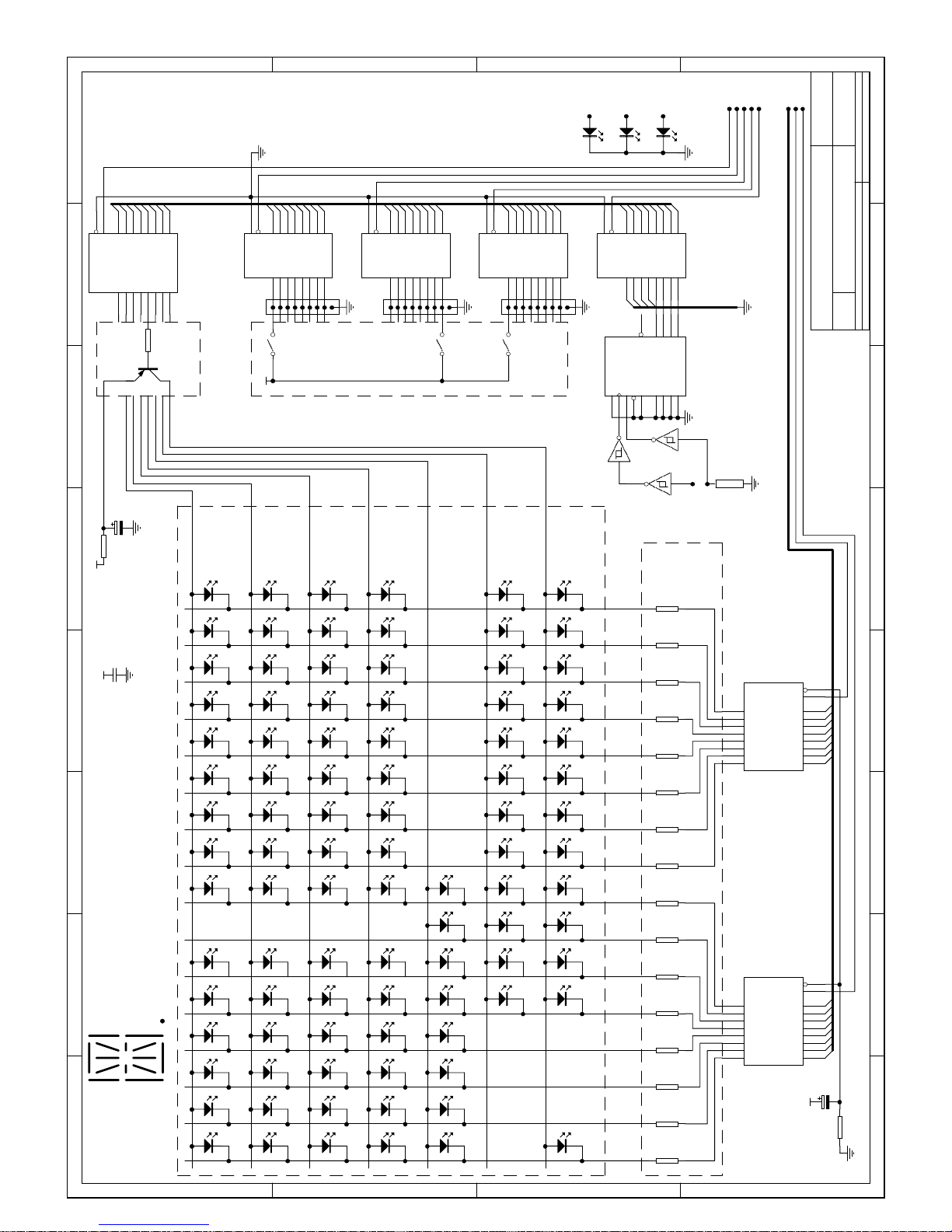
File: D:\R_&_D\HPDIMMER\CIRCUIT\Ledmtrx6.s01Drawn By:
C1,2,3,4,6
100nF
+5
SIG
LED24
LED23
LED22
C11
10uF
R25
1R
R18
100R
R16
100R
R15
100R
R14
100R
R11
100R
R10
100R
P04P112P213P33PE1CIN5U/D10CLK15RST
9
Q06Q111Q214Q3
2
COUT
7
IC9
4516
1213
IC8F
40106
+5
C5
10uF
R24
10k
R17
100R
Q1-Q7
BCX17
C8GC12G C11G C9G C7G C6G C5G C4G C3G C2G C1G
C8RC12R C11R C9R C7R C6R C5R C4R C3R C2R C1R
RUNCHAN MODE TEST
C10R
C10G
BLD CLR NORMBANK
N4 C4F4G4H4J4P4A4DP4M4L4K4D4E4 B4
N3 C3F3G3H3J3P3A3DP3M3L3K3D3E3 B3
N2 C2F2G2H2J2P2A2DP2M2L2K2D2E2 B2
B1E1 D1 K1 L1 M1 DP1 A1 P1 J1 H1 G1 F1 C1
1 2
IC8A
40106
R1-R7
100R
+5
+5
S1-S8
S9-S12
A02A13A24A35A46A57A68A7
9
B018B117B216B315B414B513B612B7
11
E
19
DIR
1
IC4
74HC245
A02A13A24A35A46A57A68A7
9
B018B117B216B315B414B513B612B7
11
E
19
DIR
1
IC5
74HC245
A02A13A24A35A46A57A68A7
9
B018B117B216B315B414B513B612B7
11
E
19
DIR
1
IC6
74HC245
OC
1
C
11
1D22D33D44D55D66D77D88D
9
1Q192Q183Q174Q165Q156Q147Q138Q
12
IC1
74HC574
OC
1
C
11
1D
2
2D
3
3D
4
4D
5
5D
6
6D
7
7D
8
8D
9
1Q
19
2Q
18
3Q
17
4Q
16
5Q
15
6Q
14
7Q
13
8Q
12
IC3
74HC574
OC
1
C
11
1D
2
2D
3
3D
4
4D
5
5D
6
6D
7
7D
8
8D
9
1Q
19
2Q
18
3Q
17
4Q
16
5Q
15
6Q
14
7Q
13
8Q
12
IC2
74HC574
N1
S13-S20
A02A13A24A35A46A57A68A7
9
B018B117B216B315B414B513B612B7
11
E
19
DIR
1
IC7
74HC245
3 4
IC8B
40106
R19
100R
R20
100R
R21
100R
R22
100R
R9
100R
R8
100R
R12
100R
R13
100R
R23
100R
R26
100K
Segment Layout
dp
p
n
m
l
k
j
h
gf
e
d
c
b
a
8,9,10
PHASEC
PHASEB
PHASEA
ENCB
ENCA
LCHCDATA
FC2
FC1
FC0
A19
BGACK
10K
10K
RN3
RN2
RN1
S21
22
HP Dimmer Front PCB
Channel
Channel
Normal
Clear
Run
Build
Test
Mode
Chan
Bank
spare
spare
spare
enter
ch12
ch11
ch10
ch9
ch8
ch7
ch6
ch5
ch4
ch3
ch2
ch1
Keypad
Green
Red
Digit 4
Digit 3
Digit 2
Digit 1
Drive
D.Timmins
1265.82/B4.2
JANDS
10K
6
Page 29

Equipment Description 3-11
Revision 2 - 26 April, 2000 HP SERIES DIMMER TECHNICAL MANUAL
3.7 Front panel card
(
Figure 3.4
The front panel PCB holds all front panel switches and LEDs, including the LOAD and
DRIVE LEDs which are fed by the Output PCB. Additionally, the control electronics for
the switches and LEDs and the encoder circuitry are also on the front panel PCB. To
minimise flat cable size, the CPU da ta bus and req uired CPU selec t lines are connected to
the front panel card to control the latches for the LEDs and buffers for the
switches/encoder circuitry. The majority of components on t his card are Surface Mo unt
devices.
3.7.1 Switches
The switches are read individually via tri-state 74HC245 buffers (IC4, IC5, IC6). E ach
switch when pressed (closed) pulls the buffer input high, ot herwise a 10K resistor (RN1,
RN2, RN3) pulls it to ground.
Note that switch faults will most likely be caused through wear in the switches
themselves.
3.7.2 LEDs
Due to t he large number of front panel LEDs (including the four 15 segment displays),
all except the Phase LEDs and Drive/Load LEDs are driven in a matrix, the seven rows
of which are driven by a 74HC574 latch and BCX17 transistors (IC1/Q1-7/R1-R7). T he
16 columns are driven by two 74HC574 latches (IC2-3/R8-23). T he matrix is driven with
only one row o n at any time, each row being on for approximately 2ms out of 14ms. A
failu r e in t he matr ix c o uld r e su lt in a r o w be ing d e ad (e g . D ig it 1 o r Gr e e n S e le ct LE D s
off) or a co lumn be ing d ead (eg . seg ment 4 o f all dig its fa iled) , els e th e fault will be a
single LED dead. It is import ant when tracing matrix faults to refer directly to t he circuit
diagram.
Note that the bicolour “Select” LEDs are sensitive to excess so ldering temperature and
should be replaced with care.
An RC delay networ k C5/R24 holds the display off for a short period during startup t o
ens ur e t h e C PU has t ime t o init ialis e t he ma t rix befo r e t he dis pla y be co mes a ct ive . Th is
prevents damage to the display LEDs through over current and ensures that the large
current required to feed all segments does not occur .
An RC decoupling network C11/R25 minimises the amount o f noise generated by the
LED multiplex circuit that is fed into the 5 vo lt r ail.
3.7.3 Encoder
The encoder output consists of two signals 90 degrees out of phase. These signals have
already been filtered on the CPU card, and so are then squared by a 40106 Schmitt
(IC8:A/:B/:C). The signals are used to control the 4516 up/down co unter (IC9) such that
when the encoder is rotated clockwise the counter co unts up,and when the encoder is
rotated counterclockwise the counter counts down. Note that any time the encoder is
rotated, pulses should appear on pins 10 and 15 of the counter IC9.
Page 30

[1]
DISPLAY = "Select channels for
60V"
[2]
[4]
[5]
[6]
[7]
DISPLAY = "Select chans for
Preheat off"
DISPLAY = "Select channels for
120V"
Status LED red = 60V or 120V
Status LED green = 240V
Status LED orange = Channel
selected for output voltage change
DISPLAY = "Select chans for
Linear-Power"
DISPLAY = "Select chans for
Switched Output"
DISPLAY = "Select chans for
Preheat on"
ENTER
ENTER
ENTER
ENTER ENTER
NORMAL
ENTER
ENTER
ENTER
ENTER
[2]
ENTER
[3]
ENTER
ENTER
ENTER ENTER
Voltage Temperature
Current core temperature
[Voltage choice for selected channel Voltage choice for selected channel
ENTER
ENTER
SELECT
STATUS
SELECT
STATUS
SELECT
STATUS
120V selection applied 240V selection applied
SELECT
STATUS
SELECT
STATUS
SELECT
STATUS
MODE
MODE
[START]
ENTER
ENTER
ENTER
Power Fault
Neutral detect "On"
ENTER
ENTER
Neutral detect "Off"
Neutral detect "On" selection applied Neutral detect "Off" selection applied
Law
Linear-Power Switched Output
[4]
[5]
Linear-Power selection applied Switched output selection applied
Preheat
Preheat "On"
Preheat "Off"
[6]
[7]
Preheat "On" selection applied Preheat "Off" selection applied
ENTER
SELECT
STATUS
Preheat "Level"
[8]
Preheat level set
ENTER
[9]
To
"TERM"
[8]
DISPLAY = "Press select and hold
while changing channel preheat"
[9]
DISPLAY = "A"
(a letter between A and E)
ENTER
ENTER
[1]
Voltage choice for selected channel
60V selection applied
SELECT
STATUS
[3]
DISPLAY = "Select channels for
240V"
[Hold while
setting level]
MODE 1: VOLTAGE, TEMPERATURE, LAW, PREHEAT, VOLTAGE FLUCTUATION
(Termination, Check, Voltage Compensation & Lock to be continued next page)
Figure 4.1 A
Page 31

Dimmer Operation 4-1
Revision 2 - 26 April, 2000 HP SERIES DIMMER TECHNICAL MANUAL
4.0 Dimmer Operation
Th is s e c tio n a s s umes the d imme r ha s b e e n c orrec tly c o n n e c ted to thr e e p h a s e p owe r an d
a source of DMX input signals.
4.1 Menu structure
Th e HP dimmer s feat ur e a “t ree” menu structure. This means that an option is chosen
from the display with the LEVEL/FUNCTION encoder wheel, and the ENTER keypad
butto n is then pressed to confirm the selection.
The encoder wheel is then used to select t he next level of options, t he ENTER bu t to n is
pressed to confirm the selection, and so on.
After all the options have been selected, the display reverts to “OK” to indicate the
dimmer is n ow back in norma l operating mo de.
Th e dis play w ill flash if there are mor e menu levels above the cu rrent one.
4.1.1 E NTER
The ENTER keypad button is always pressed to confirm a menu or channel selection.
4.1.2 N ORMAL
The NORMAL keypad button cancels the current menu selection and allows the
operat or to start again in the event of an error. The display shows “OK”.
Pressing NORMAL wh ile “OK” is d isp layed sho ws th e d immer so ftw ar e ve rs ion.
DIP
switch 1 on the CPU card is u sed to specify t he type of dimmer as follows:
DIP Switch #1 Product Version Display
Off TR/SC “TRSC V2. 2 … ”
On Original HP “HP V2.2 ….”
Th e DIP switch is chec ked at startup and the dimmer configured accordingly.
4.1.3 CLEAR
The CLEAR keypad bu tton is u s e d to g o b a c k on e me n u le v e l if a n option is in c orr ectly
selected.
4.1.4 MODE menu
(
Figure 4.1A
Select the MODE bu tt o n o n t he ke yp ad . T he dis pla y will t he n “f lash ” s ho win g o ne o f
the MODE options, which are:
• “VOLT” - out put voltage selection
• “TEMP” - heatsink temperature monitor
• “LAW” - dimmer law
• “PREH” - filament prehea t
• “P.FLT” - mains input voltage fault (power fault) test enable
Page 32

Dimmer Operation 4-2
Revision 2 - 26 April, 2000 HP SERIES DIMMER TECHNICAL MANUAL
• “TERM” - DM X input termination
• “CHEK” - display dimme r o perating parameters
• “V.COM”- enable/calibrate voltage compensation
• “LOCK” - lock dimme r functions
To select an option, rotate the FUNCTION encoder wheel until the desired option is
displayed, then press the ENTER keypad butt on to confirm the selection.
4.1.4.1 “VOLT” - Voltage selection
(
Figure 4.1A
Any or a ll of t h e d imme r cha n nels ma y be c u s to mis e d to g ive eithe r 240, 120, o r 60
vo lt o ut pu t. This feat ur e is use ful fo r c ont r olling indiv idua l 120 volt loads, such as
single PAR 64 (120) lamps, Leko (FEL) or other 120 volt lamps (120V), o r series
pairs of ACLs (60V).
• Once the VOLT option has been selected, use the FUNCTION encoder wheel
to select either “240V”, “120V”, or “60” and press ENTER.
• If “240V” is se le ct e d , t he d isp la y w ill st op fla s hing a nd w ill s c r o ll t h e fo llo w ing
message: “SELECT CHANNELS FOR 240V”.
• If “120V” is se le ct e d , t he d isp la y w ill st op fla s hing a nd w ill s c r o ll t h e fo llo w ing
message: “SELECT CHANNELS FOR 120V”.
• If “60V” is sele ct ed, t he d ispla y will st o p fla shing and will s cr oll t he fo llow ing
message: “SELECT CHANNELS FOR 60V”.
• Press the SELECT butto n on t he channel to be changed. The STATUS LED o f
t h e channel(s) selected will change colour to orange.
• Once all the required channels are selected, press ENTER t o make the changes.
The channel STATUS LE D(s ) w ill sho w g ree n fo r t ho se c hann el(s ) s et t o 240
volt output, and red for t hose channel(s) set to 60 or 120 volt output.
• The display will then show “OK” to indicate the dimmer is now in normal
operat ing mode with the selected changes implemented.
CAUTION
SELECTING A 60 or 120 VOLT LAMP TO 240 VOLT
OPERATION CAN CAUSE SERIOUS DAMAGE TO THE LAMP !
4.1.4.2 “TEMP” - Temperature monitor
(
Figure 4.1A
The internal heatsink temperature may be monitored by selecting “TEMP”. The
display shows the temperature in degrees Celsius, eg “24ºC”. Normal DMX
operation of the dimmer is unaffected by selecting this function. Pressing the
NORMAL bu tton on the keyp ad will clear the disp lay to “OK”.
Note
The HP12-TR / HP12-SC / HP6-C dimmers are designed to be installed in
standard 19-inch wide racks. These racks should have adequate ventilation
allowing for the side-to-sid e airflow of the dimmers. Fully enclosed racks that
obstruct side-to-side ventilation may cause overheating problems.
Page 33

Fault Diagnosis 4-3
Revision 2 - 26 April, 2000 HP SERIES DIMMER TECHNICAL MANUAL
4.1.4.3 “LAW” - Dimmer law
(
Figure 4.1A
Selecting “LAW” gives the opt ion of either a linear power curve - “Lin P” - or a
switch curve - “Swch”. The linear power curve gives even fade characteristics for
lamps, while t he switch cur ve may be used for switching other devices (eg. fans,
stro bes, motor s, etc) o n or o ff, with the switching points set at 55% for upfades and
45% for downfades.
• Use the FUNCTION encoder wheel to change the law, and press ENTER to
select.
• Next press t he channel SELECT butto ns to select the channels to be changed.
The channel STATUS LE Ds w ill flash. Press ENTER to make the changes.
• The display will change to “OK” to indicate the dimmer is now in normal
operat ing mode with the selected changes implemented.
4.1.4.4 “PREH” - Filament preheat
(
Figure 4.1A
If a cha nnel is fu lly loa ded , t here is a po ssibilit y t hat co ld filame nt inru sh cu rr ent
may cause nuisance tripping of the circuit breakers. If this is a problem, t he pr eheat “PREH” - option may be used to r educe the inrush. When preheated, t he filaments
may show a barely perceptible dull orange glow.
Preheat has no effect when the lamp is being driven above the preheat level or for
channels set to switched output. See section 5.6 for an explanation of cold filament
inrush current.
• Selecting “PREH” gives the options of “ON”, “OFF”, and “LEVL”. Use the
FUNCTION encoder wheel to choose t he opt ion and press ENTER to confirm
selection. Selecting “LEVL” allows the control of the preheat level for each
channel regardless of whether preheat is turned on or off for that channel.
When “ON” or “OFF” has been selected:
• Press the channel SELECT button(s) to select preheat for the desired
channel(s).
• The channel STATUS LE D( s) will “fla sh” w hen th at cha nnel is sele ct ed . P res s
ENTER to make the change(s).
• The display will change to “OK” to indicate the dimmer is now in normal
operat ing mode with the selected change implemented.
When “LEVEL” has been selected:
• Press and hold the channel SELECT button for the desired channel. While
holding SELECT button adjust the encoder wheel to set the desired preheat
level. Preheat is adjustable in 5 leve ls from A (lowest) to E (highest).
• Press ENTER to make the change(s) permanent.
• The display will change to “OK” to indicate the dimmer is now in normal
operat ing mode with the selected change implemented.
Normal DMX operation of the dimmer is unaffected b y selectin g this fun ction.
Page 34

Dimmer Operation 4-4
Revision 2 - 26 April, 2000 HP SERIES DIMMER TECHNICAL MANUAL
4.1.4.5 “P. FLT” - Mains Power Fault
(
Figure 4.1A
Th e HP series dimmers will detect two types of main s supply problems:
• Mains undervoltages
• Neutral-to- ear th overvoltage
In some venues the three phase power supply may be less than ideal, and one or
more of the above fault conditions may occur without the wiring being truly
“faulty”. For this reason it is possible (BUT NOT RECOMMENDED) to use the
P.FLT option to turn off the power fault detect (the show must go on). ALWAYS
check first that the problem is not a dropped neutral in either of the three phase
connectors, or a missing earth connection.
WARNING
IF THE NEUTRAL DETECT FACILITY IS DISABLED, IT IS PO S S IBLE
THAT UNSAFE MAINS SU PPLY WIRING MAY NOT BE DETECTED.
The HP dimmers will tolerate and even correct for mains supply problems of
sufficient magnitude to damage less tolerant equipment connected to the same
supply. The HP dimmer de t ec tio n fac ilitie s ma y be use d t o p ro vid e " ea r ly wa rn ing "
pr o te ct io n fo r anc illar y eq uip men t. S ec tio n 5 . 1. 3 g ive s a mor e in- de pt h exp lana t io n
of this facility.
• Selecting “P.FLT” gives the options of “ON” or “OFF”. Use the FUNCTION
encoder wheel to choose the option and press ENTER to confirm selection .
• The display will change to “OK” to indicate the dimmer is now in normal
operat ing mode with the selected change implemented.
Normal DMX operation of the dimmer is unaffected b y selectin g this fun ction.
Page 35

Fault Diagnosis 4-5
Revision 2 - 26 April, 2000 HP SERIES DIMMER TECHNICAL MANUAL
[ BLANK PA GE ]
Page 36

MODE 2: TERMINATION, CHECK, VOLTAGE COMPENSATION & LOCK
[10]
DISPLAY = "CH1*DMX-1*Level-
19*Volt-240*Law-Linear power*
Preheat-Off*Preheat value-
E*Status-Enabled"
ENTER
ENTER
ENTER
ENTER
ENTER
ENTER
ENTER
Voltage compensation applied Voltage compensation not applied
DMX Termination
Term "On" Term "Off"
DMX terminated DMX not terminated
From
"P.FLT"
[10]
ENTER
ENTER
ENTER
ENTER
Dimmer Parameter Readout Mains Voltage Compensation
ENTER
ENTER
Dimmer locked
ENTER
ENTER
Dimmer unlocked
Turn left for
1 step
Turn right for
1 step
Turn right for
1 step
Dimmer user lock
NORMAL
Adjust to scroll
through channel
Figure 4.1 B
Page 37

Dimmer Operation 4-6
Revision 2 - 26 April, 2000 HP SERIES DIMMER TECHNICAL MANUAL
4.1.4.6 “TERM” DMX Signal Terminate
(
Figure 4.1B
Selecting “TERM” allows the DMX signal to be correctly terminated, as is
re q uir e d fo r t he las t d imme r in a D M X lin e. N o t e t h at w he n s e t t o “ON” the DMX
Loop co nnecto r in unused.
Pressing the NORMAL bu tt o n o n th e ke ypa d w ill cha nge the dis play t o “OK” to
indicate the dimmer is no w in normal operating mode.
4.1.4 .7 “CHE K” dimmer operating parameter display
(
Figure 4.1B
Selecting “CHEK” displays the dimmer’s operating parameters on a channel by
channe l b asis. This is useful for checking that a dimmer has b een set up corre ctly.
Select the channel to be checked by turning the FUNCTION encoder wheel (the
STATUS LE D of t he channel being check ed will fla sh). Stop the scrolling of t he
dis p la y a t an y time by p res s ing ENTER. Press ENTER and tur n the encoder wheel
at th e s a me time to d is play information “v e r tically”, ie . dis p lay t h e same in forma tio n
for diffe rent channels .
Pressing the NORMAL bu tt o n o n th e ke ypa d w ill cha nge the dis play t o “OK” to
indicate the dimmer is no w in normal operating mode.
Normal DMX operation of the dimmer is unaffected b y selectin g this fun ction.
4.1.4.8 “V.COM” Output voltage Compensation
(
Figure 4.1B
An H P dimme r ca n be s etu p so th at it will c omp ensa te fo r v aria tio ns in t he ma ins
input voltage. Selecting “V.COM” allows the internal voltage compensation to be
turned on or off, or calibrated. After a Deep Clear, V.COM defaults to Off.
• Selecting “V.COM” gives the options of “ON”, “OFF”, “LINE” and
“MAX”. Use the FUNCTION encoder wheel to choo se the desired opt ion and
press ENTER t o confir m s e le c tio n . Sele c ting “LINE” allo w s c alib r at ion fo r t h e
voltage compensation, while selecting “MAX” allows set ting of the maximum
out put voltage the dimmer regulates t o.
When “ON” or “OFF” has been selected:
The dis play will c hang e to “OK” to ind icate the dimmer is now in normal oper ating
mode with the selected change implemented.
When “LINE” has been selected:
• Note that an external voltmeter is necessary to complete this procedure.
This parameter should not need to be adjusted during normal operation.
Adjust the d is p layed volt a ge u s ing th e FUNCTION encoder wheel until it reads
the same as the current input voltage, as displayed on the voltmeter. It is
recommended that all phases be driven from a single phase source eg. via a
single to three phase adaptor, to eliminate phase voltag e variations.
• Press ENTER to calib rate the dimmer.
• The display will change to “OK” to indicate the dimmer is now in normal
operat ing mode with the selected change implemented.
Page 38

Dimmer Operation 4-7
Revision 2 - 26 April, 2000 HP SERIES DIMMER TECHNICAL MANUAL
When “MAX” has been selected:
• Adjust the displayed voltage using the FUNCTION encoder wheel until it is
eq ual t o t he d esir ed max imum o utp ut volt age fro m th e dimme r w hen d rive n to
full. eg to avoid running 220 volt lamps above their rated voltage set this
parameter to 220V.
• Press ENTER to set t h e maximum output vo ltage fr om the d immer.
• The display will change to “OK” to indicate the dimmer is now in normal
operat ing mode with the selected change implemented
Note that the voltage compensa tion system works within th e followin g limitations :
1. The output cannot be driven above the input voltage. eg if the MAX value is
set to 240, and the mains input voltage is 220, the maximum voltage available
at the output is 220 volts.
2. The compensation system does not operate on switched output s (ie. channels
with dimmer law set to “ switch”).
3. Th e dimme r must be correctly calibrated a s outlin ed a bove.
Norma l D M X ope ration of t he dimmer is u n a ffe c ted b y this p r oce d ure , howe ve r t h e
dimmed output level may change due to normal operation of the compensation
system.
4.1.4.9 “LOCK” Parameter Lockout Facility
(
Figure 4.1B
If the d imme r is t o be le ft un a tt e nded it is s ometimes des ir a b le to be able to lock the
settings such that unauthorised users cannot alter them. The “LOCK” option
prov ides this facility.
• Selecting “LOCK” gives the single option of “ON”. Pressing ENTER locks
t h e dimme r, and “LOCK ” is disp layed .
• To u nlo ck a d immer , t ur n t he FUNCTION encoder wheel one step to t he left,
press enter, o ne step t o t he right, press enter, and finally one step to t he right. If
a mistake is made during the unlock procedure, turn the wheel more than three
steps to the right to reset the sequence and try again.
• Whe n the dimme r has been unlocked it will disp lay “OK”.
Normal DMX operation of the dimmer is unaffected b y selectin g this fun ction.
Page 39

Fault Diagnosis 4-8
Revision 2 - 26 April, 2000 HP SERIES DIMMER TECHNICAL MANUAL
[ BLANK PA GE ]
Page 40

[1]
Repeat for each channel to be tested.
All remaining channels will operate
as normal.
[2]
Will display bank number in blocks
of 12 channels (6 channels for HP6)
After a deep clear, it is necessary to
reprogram the dimmer to indicate
output voltage 110V or 240V and
number of channels (12 for HP12).
Status LED red = 110V
Status LED green = 240V
[3]
For DEEP CLEAR. Turn off power.
Hold MODE and DMX BANK simul-
taneously while turning on power.
HP DIMMER MS-9507-02
TEST
NORMAL
[Exit to DMX operation]
TEST
LEVEL
SELECT
STATUS
DMX BANK
ENTER
[DMX BANK selected ]
DMX BANK
FUNCTION
[Selected DMX BANK value]
DMX CH.
ENTER
[DMX start number selected ]
DMX CHANNEL
[Selected DMX start channel]
FUNCTION
[1]
[2]
[DMX start level ]
[DMX BANK No. ]
DMX BANK
MODE
FUNCTION
ENTER
FUNCTION
ENTER
[Selected output voltage]
[Number of channels for dimmer]
[Exit to DMX operation ]
DEEP CLEAR
[3]
POWER
[START] [START]
[DMX BANK value]
[DMX start channel]
[START]
[START]
[Selected output voltage]
[Number of channels for dimmer]
TEST, DMX BANK, DMX CHANNEL, DEEP CLEAR
Figure 4.2
Page 41

Dimmer Operation 4-9
Revision 2 - 26 April, 2000 HP SERIES DIMMER TECHNICAL MANUAL
4.1.5 DMX CHannel menu
(
Figure 4.2
Th e d imme r ’s DM X star t c ha nn e l ca n b e s e lec t e d an ywh er e fr o m c ha nn el 1 t o ch a nne l
512. By selecting DMX start channel 1, the dimmer will r esp o nd t o D MX cha nnels 1
through 12 inclusive. When using racks of loo ped dimmers, the next dimmer sho uld
start at channel 13, the next at channel 25, and so on.
• To select a DMX st ar t channel press the DMX CH button on the keypad.
• Th e dis play will cha nge to show the curre ntly assigned DMX star t channel.
• Using the FUNCTION encoder wheel, the DMX start channel may be
incremented or decremented to the desired DMX channel start number.
• To select t he DMX st ar t channel press the ENTER button on the keypad.
• The display will then show “OK” to indicate the dimmer is now in normal
operat ing mode.
4.1.5.1 Channel Softpatch (Software version 2.2 and later)
Dimme r ch anne ls ma y now be p at che d t o the inco ming DM X s igna l in a ny o rd er. T o
patch a channel:
• Press the “DMX Ch” button. The dimmer will respond with the normal DMX
start.
• Press the “Select” button of the channel to be non-sequentially patched. The
“Status” LED will flash and the display will indicate what DMX channel that
dimmer is currently patche d to.
• Use the wheel to adjust display to desired channel, and press “Enter” to confirm.
Note that adjusting the DMX Bank or DMX Ch without pressing a channel select
butto n resets all channels to being sequential and clears any previous patch information.
4.1.6 DMX BANK menu
(
Figure 4.2
To make DMX start channel selection easier, the HP dimmers can select a bank of
twelve channels [six channels] from the DMX input signal. There are a total of 42
sequential banks of twelve channels and one last bank of eight channels in the 512
channels available from the DMX-512 source. See section 8.2 for a list of banks and
their corresponding channels.
By selec ting DMX s tar t ba nk 2, the d imme r will r e s p ond to DMX c h a n nels 1 3 thr oug h
24 [13 – 18] inclusive.
• To select a DMX bank press the DMX B ANK button on the keypad.
• Th e dis play will cha nge to show the curre ntly assigned DMX ban k number.
• Using the FUNCTION encoder wheel, DMX bank numbers may be incremented
or decremented to the desired bank number.
• To select t he DMX bank number press the ENTER button on the keypad.
• The display will then show “OK” to indicate the dimmer is now in normal
operat ing mode.
Page 42

BUILD: SNAP 1~3, SCENE 1 & 2
BUILD
ENTER ENTER
ENTER
ENTER
[1]
[1]
DISPLAY = "Press Enter to store DMX
value"
[2]
DISPLAY = "Press Select and hold
while change level for each channel"
[DMX snapshot recorded] [Local scene recorded]
[2]
[SC1: SCENE1 / SC2: SCENE 2]
[SP1: SNAP1 / SP2: SNAP2 / SP3: SNAP3]
[3]
Repeat step for each channel to be
included in selected Scene
[3]
[Channel level]
BUILD
SELECT
STATUS
Status LED red = 110V
Status LED green = 240V
[START]
HP DIMMER MS-9507-03
Figure 4.3
Page 43

Fault Diagnosis 4-10
Revision 2 - 26 April, 2000 HP SERIES DIMMER TECHNICAL MANUAL
4.1.7 BUILD menu
(
Figure 4.3
The BUILD menu is used to record DMX Snapshots or user-defined Scenes.
• Press the BUILD keypad bu tton.
• Select a flashing Snapshot number (“SP1 - SP3”) or a Scene number (“SC1 -
SC2”) to record, using the FUNCTION encoder wheel.
• Press ENTER to confirm the selection.
4.1.7.1 Snapshot
(
Figure 4.3
Once a SNAPSHOT number is selected (“SP1”, “SP2” or “SP3”), t he d isp la y w ill
sc ro ll the mess age : “PRESS ENTER TO STORE DMX VALUE”.
• On pressing ENTER, the dimmer will store the current DMX values for the
t welve dimmer channe ls in t he currently se lected bank .
• The display will change to “OK” to indicate the dimmer is now in normal
operat ing mode.
4.1.7.2 Scene
(
Figure 4.3
Once a Scene (“SC1” or “SC2”) is selected, the disp lay will scroll the message:
“PRESS SELECT AND HOLD WHILE CHANGE LEVEL FOR EACH
CHAN”.
• For each channel required to Build the Scene, press and hold the SELECT
button.
• Th e dis play w ill initially show the last recorded level fo r that c hannel, which may
then be changed by rotating the LEVEL/F UNCTION encoder wheel.
• Once all the required channels have been changed, press ENTER t o c o nfir m the
changes.
• The display will change to “OK” to indicate the dimmer is now in normal
operat ing mode.
Page 44

RUN: SNAP 1~3, SCENE 1&2, PRE-RECORDED CHASES 1~6
[1]
DISPLAY = "SP1 on level 100"
"SP2 on level 100"
"SP3 on level 100"
[2]
[3]
DISPLAY = "SC1 on level 100"
"SC2 on level 100"
DISPLAY = "PR1 run 100 B.P.M."
"PR2 run 100 B.P.M."
"PR3 run 100 B.P.M."
"PR4 run 100 B.P.M."
"PR5 run 100 B.P.M."
"PR6 run 100 B.P.M."
[4]
Press SELECT and hold while
adjusting channel level via level
control.
This step removes the selected
channel from a SNAP, SCENE or
PRE-RECORDED CHASE and
enables the channel level to be
adjusted in isolation. These new
levels are not stored.
Status LED red = 110V
Status LED green = 240V
HP DIMMER MS-9507-04
ENTER
NORMAL
[Stand alone channel level]
[over all Level of SNAP]
[SP1: SNAP1 / SP2: SNAP2 / SP3: SNAP 3]
RUN
RUN
SELECT
STATUS
SELECT
STATUS
ENTER
[Stand alone channel level]
[over all Level of SCENE]
SELECT
STATUS
SELECT
STATUS
ENTER
[Stand alone channel level]
[Speed in B.P.M.]
SELECT
STATUS
SELECT
STATUS
NORMAL NORMAL
[SC1: SCENE1 / SC2: SCENE2]
[Exit to DMX operation] [Exit to DMX operation] [Exit to DMX operation]
[1] [2]
[3]
[4] [4]
[4]
[PR1 -PR6: Prerecorded chases]
[START]
[Speed]
Figure 4.4
Page 45

Fault Diagnosis 4-11
Revision 2 - 26 April, 2000 HP SERIES DIMMER TECHNICAL MANUAL
4.1.8 RUN menu
(
Figure 4.4
Th e H P d imme rs o ffe r a r a n g e of pr e-r e c orded S n a p s hot s , Sce ne s a n d C hases that ma y
be u sed for tes ting pur po ses o r fo r wh en t he d immer r ack is u sed in st and -alo ne (no
contro l desk) applications.
The Snapshots and Scenes must be recorded via the Build menu (see section 4.1.7).
The Chase patterns are factory-set and cannot be changed. The output levels of
Snapshots and Scenes may be varied with the LEVEL/FUNCTION encoder wheel,
which becomes a master level control. During chases the encoder wheel becomes a
chase rate cont r ol.
In all cases, individual channel levels may be changed. Once changed, however, they
remain at the n ew le vel regardless of the s etting of the master level contr ol.
No te t hat any p revio usly dis abled cha nnels w ill rema in disabled w hen in R UN mo de,
with chase sequences abbreviated to avoid visible gaps.
• To run a Snapshot, Scene or Chase, press t he RUN keypad butto n.
• Select either a Snapshot (“SP1”, “SP2”, or “SP3”), a Scene (“SC1” or
“SC2”), or a Fact ory Preset Chase (“PR1”, “PR2”, “PR3”, “PR4”, “PR5”, or
“PR6”) with the FUNCTION encoder wheel.
• Press ENTER to confirm the selection.
4.1.8.1 Snapshot
(
Figure 4.4
If Snapshot 2 (“SP2”) is s e le c ted , t he disp la y w ill s c roll with the me s s a g e “SP2 ON
LEVEL 100”.
• The output level may be altered with the LEVEL/FUNCTION encoder wheel
and the display will indicate a level b etwee n 100% and 0%.
• Pressing a channel SELECT button will isolate that channel from the master
level control. The STATUS LED will flash to show the channel is isolated.
Pressing the SELECT bu tton again will re-connect the channel t o the master
level cont ro l.
• By pressing and HOLDING a channel SELECT button, and rotating the
encoder wheel, that channel level may be modified.
Note
The master level control no longer has any effect on the level of a modified
channel; ie. once a channel has been modified, it remains at that level while
still in RUN mode (regardless of the master level). The channel SELECT
button must pressed again to re-connect that channel to the master level
control.
• Once the SELECT button is released, the encoder wheel becomes the master
level cont ro l onc e more.
Page 46

Fault Diagnosis 4-12
Revision 2 - 26 April, 2000 HP SERIES DIMMER TECHNICAL MANUAL
4.1.8.2 Scene
(
Figure 4.4
If Scene 1(“SC1”) is se lect ed, the disp lay will s cro ll wit h th e mess age “SC1 ON
LEVEL 100”.
• Th e o v er a ll o u t p u t le ve l may b e a lt e r ed w it h t he LEVEL/FUNCTION encoder
wheel a n d t he display will indicate a level b etween 100% and 0%.
• Pressing a channel SELECT button will isolate that channel from the master
level control. The STATUS LED will flash to show the channel is isolated.
Pressing the SELECT bu tton again will re-connect the channel t o the master
level cont ro l.
• By pressing and HOLDING a channel SELECT button, and rotating the
encoder wheel, that channel level may be modified.
Note
The master level control will no longer have any effect on the level of the
modified channel; ie. once a chan nel has been modi fied, i t remains at that level
while still in RUN mode (regardless of the setting of the master level). The
channel SELECT button must p ressed again to re-connect that chan nel to the
maste r level cont ro l.
• Once the SELECT button is released, the encoder wheel becomes the master
level cont ro l onc e more.
4.1.8.3 Preset chases
(
Figure 4.4
If Preset Chase 4 (“PR4”) is selected, the display will scroll with the message
“PR4 RUN 100 b.P.M.”.
• The chase rate may be altered with the FUNCTION encoder wheel and the
dis play will indic ate a rat e between 6 and 600 beats per minute.
• By pressing and HOLDING a channel SELECT button, and rotating the
encoder wheel, that channel level may be edited.
• Once the SELECT butto n is released, the encoder wheel becomes the chase rate
control once more . Th ere is no master level co ntrol for this function.
The factory Preset Chase patterns for HP12 [HP6] are as follows:
PR1 Channels 1 to 12 [6] in sequence (12 [6] step chase)
PR2 Channels 12 [6] to 1 in sequence (12 [6] step reverse chase)
PR3 Channels 1 to 12 [ 6] in sequence (12 [6] step shado w chase) ie. chase channel off
PR4 12 [6] Cha nne l Ra ndom chase
PR5 Channels 1 & 2 crossfade to Channels 3 & 4.....(6 [3] step 2-channel x-fade)
PR6 Channels 1, 2, 3 crossfade to Channels 4, 5, 6....(4 [2] step 3-channel x-fade)
Page 47

Fault Diagnosis 4-13
Revision 2 - 26 April, 2000 HP SERIES DIMMER TECHNICAL MANUAL
[ BLANK PA GE ]
Page 48

[1]
Repeat for each channel to be tested.
All remaining channels will operate
as normal.
[2]
Will display bank number in blocks
of 12 channels (6 channels for HP6)
After a deep clear, it is necessary to
reprogram the dimmer to indicate
output voltage 110V or 240V and
number of channels (12 for HP12).
Status LED red = 110V
Status LED green = 240V
[3]
For DEEP CLEAR. Turn off power.
Hold MODE and DMX BANK simul-
taneously while turning on power.
HP DIMMER MS-9507-02
TEST
NORMAL
[Exit to DMX operation]
TEST
LEVEL
SELECT
STATUS
DMX BANK
ENTER
[DMX BANK selected ]
DMX BANK
FUNCTION
[Selected DMX BANK value]
DMX CH.
ENTER
[DMX start number selected ]
DMX CHANNEL
[Selected DMX start channel]
FUNCTION
[1]
[2]
[DMX start level ]
[DMX BANK No. ]
DMX BANK
MODE
FUNCTION
ENTER
FUNCTION
ENTER
[Selected output voltage]
[Number of channels for dimmer]
[Exit to DMX operation ]
DEEP CLEAR
[3]
POWER
[START] [START]
[DMX BANK value]
[DMX start channel]
[START]
[START]
[Selected output voltage]
[Number of channels for dimmer]
TEST, DMX BANK, DMX CHANNEL, DEEP CLEAR
Figure 4.2
Page 49

Dimmer Operation 4-14
Revision 2 - 26 April, 2000 HP SERIES DIMMER TECHNICAL MANUAL
4.1.9 TEST function
(
Figure 4.2
Each channel may be tested individually, or as a group, by fading them from 0 to
100%. Any previously disabled channel may be selected and tested.
• Press the TEST keypad button and the display will s h ow “TES T”.
• Next press the desired channel SELECT buttons. This will take the selected
channel(s) off-line from the DMX input. The rema ining c hannel(s) will s tay on-line.
• The STATUS LED ( s) w ill flash t o ind ic at e w hic h c ha nn el( s ) ar e u nd e r tes t . As t h e
LEVEL/FUNCTION encoder wheel is rotated, the channel level(s) will change
from their current level.
• When all tests are completed, press t he NORMAL bu t to n. T h e d is p lay w ill c ha ng e
to “OK ” to indicate the dimmer is now back in normal operat ing mode and all
channels are once again on-line to the DMX input control signal.
4.2 Deep clear
(
Figure 4.2
In the event of a software “lockup” or error message (see section 5.2), the HP d immer s
have a facility that enab les them to be Deep Cleared.
CAUTION
THIS FUNCTION WILL ERASE THE CURRENT SETTINGS IN MEMORY
AND REQUIRES RE-INITIALISING OF THE OUTPUT VOLTAGE AND
NUMBER OF CHANNELS. ENS URE TH AT TH E VOLTAG E IS S ET TO 1 20
VOLTS IF RUNNING ANY 120 VOLT LAMPS, OR DAMAGE TO THE
LAMPS MAY RESULT.
• Hold down the MODE and DMX BANK but tons while turning power ON to
t h e dimme r.
• Use the FUNCTION encoder wheel to select either “120V” output or
“240V” output on the display and press ENTER. Individual channel output
voltage may be changed later via the MODE menu (see section 4.1.4.1).
• Next use the encoder wheel to select “12ch” o utput for HP12-TR / HP12-SC
(“6ch” output for HP6-SC), and press ENTER.
• Th e dis play will change t o “OK ” t o ind ic a te the dimmer is n ow ba ck in n orma l
operat ing mode.
4.2.1 Quick deep clear
Holding down the three buttons MODE, DMX CH and DMX BANK while turning
power ON performs a normal deep clear, except the channel and voltage options are
bypassed and the d immer is con figured for 12 by 240V channels.
Page 50

Dimmer Operation 4-15
Revision 2 - 26 April, 2000 HP SERIES DIMMER TECHNICAL MANUAL
4.3 Channel disable
When the dimmer is in normal operating mode (“OK” showing on the display), any
channel may be taken off-line by pressing its SELECT button. Pressing the button a
se con d t ime will bring tha t channel back on-line.
The STATUS LED will be o n (r ed o r g ree n) fo r all a ctiv e cha nnels, and be o ff for all
disabled channels.
Any disabled channel(s) may still be select ed and tested with the TEST function (see
se ct ion 4 .1 .9 ). Onc e t he t es ts are co mple te and th e dimme r is back in no rma l op er at ing
mode, th e channel(s) will r esu me th eir s tatu s pr ior to being tested.
4.4 Software update
Th e operating s oftware of t h e HP dimmer may be updated via the front panel DMX input
connector. To achieve this requires the following:
• HP dimmer
• HP download kit
• IBM compatible Laptop or desktop computer
To update the software, perform the following:
1. Switc h the dimmer powe r o ff.
2. Conne ct the computer serial/COM port to t he DMX input of the dimmer, using
the download cable supplied in the download kit. Disconnect any DMX
terminators.
3. Press and hold the ENTER but t on o n th e dimme r wh ile tu rning on p ow er t o
the dimmer. Later versions of dimmer software have a “confirm” stage to
prevent unintended downloads. If the dimmer displays “CFRM”, press the
MODE but ton o n the dimme r keypa d.
4. On the PC, start t he download process by typing “download hp2_2<enter>”.
Th e d imme r ke yp a d LE D s w ill c h a s e w h ile the d own lo ad proceeds – this takes
ap p rox ima tely 4 0 se c onds . Whe n the d own load is c omple te the d imme r dis play
blan k s w h ile the d a ta is p rogra mme d int o t he F L A S H me mor y, a n d the d imme r
restarts.
The software update facility should be used with the following notes and caution s:
• The dimmer mus t be Deep Cle ared (re fer se ctio n 4. 2) a nd Ca librat ed (refer sectio n
4.1.4.8) after do wnloading new operating software.
• It is r ec omme nded t hat dimme r so ft war e no t be updat ed during a tour/show season,
unless the installed software proves unsatisfactory for normal operation.
• More th an o ne dimmer may be updat ed at a time using normal DMX cables to link the
DM X Lo op con nect or of t he fir st dimmer to the inpu t o f the next , etc . I n t his c ase
step 3 must be repeated for each dimmer, before proceeding to step 4.
• Refer to the instructions supplied with the download kit for further details.
Page 51

Disassembly 5-1
Revision 2 - 26 April, 2000 HP SERIES DIMMER TECHNICAL MANUAL
5.0 Fault Diagnosis
NOTE
Contact your authorised JANDS Distributor for repairs or servicing.
In Australia refer all repairs to an authorised JANDS service agent or return the faulty
unit in s uit able packag ing to:
JANDS ELECTRONICS Service Dept,
40 KENT Rd
MASCOT NSW 2020
AUSTRALIA
PHONE: +61-2-9582- 0909
5.1 Protection
The HP Series dimmers feature several types of protection. These can be generally
classified as:
1. output protection,
2. t h ermal pr otection,
3. overvoltage protection.
5.1.1 Output protection
Each of the output circuits is protected by a 11.5 amp [25 amp] fast-acting magnetic
circuit breaker. Thes e break ers are designed to pass t h e r ated cur ren t, but will discon n ect
the output circuit for any overload condition (the larger the overload, the quicker the
disconnection).
NOTE: T he dimmer outlet sock e ts a re r a ted at 10 [ 2 0] a mp s . Avoid load in g the dimmer
outputs beyond the socket capacity.
The breakers protect the dimmer’s output devices from short-circuit loads and faulty
wiring loo ms, a nd save on expen sive dimmer repairs. A tr ipped circu it breaker indicates a
load fa ult tha t r equ ires immediate atten tion.
Note that the triacs in the HP12-TR will survive output short circuits under most
conditions. The more rugged SCR pairs in the HP12-SC / HP6-C will survive o utput
shorts under extreme conditions (high operating temperatures, high supply fault current
availability, zero cable length from dimmer to short).
5.1.2 Thermal protection
The HP dimmers feature temperature-controlled fan cooling. As the internal
temperature of the dimmer increases, the fan speed also increases. The fan begins
turning at low speed at 30°C, and reaches maximum speed at internal temperatures
above 50°C.
Page 52

Disassembly 5-2
Revision 2 - 26 April, 2000 HP SERIES DIMMER TECHNICAL MANUAL
Th e in t e rn al h e at s ink t e mp er a t u r e is c o ns t a nt ly mo n it o r e d by t he d imme r. I f t he h ea t s ink
t e mp e ratur e rise s a bove 8 5 ºC, the d imme r will a u to ma tica lly s h u t d o wn the outpu t d rive
and display the message: “OVER TEMPERATURE XXOC”. T h e d imme r will d is pla y
t his mes sag e u nt il the te mpe rat u re d ro ps belo w 8 0º C, at whic h t ime it will r est ar t . T he
fan will cont in ue to cool t he he atsink during the shut down p eriod.
The electronic shutdown at 85°C is backed up by a 90°C buried cutout, which shuts
down power t o all electronics other than the cooling fan.
No te t hat the HP6- C / HP 12-SC's two fans w ill run s lower and qu iet er u nder aver age
operating conditions than the HP12-TR's single fan, due to the increased airflow
ca p a c ity. In addition the fa n s in wall- moun t dimmer s w ill run s lowe r and quie ter than the
fans in rack-mount dimmers d ue to in cre ased natural c onvective c ooling.
5.1.3 Supply Power fault protection
Th e H P s er ies dimme rs will d et e ct vo lt ag e p r ob lems ge ner at e d b y ph as e lo a d imb ala nce
and a poor o r missing neutral connection. A poor ( r esistive) neutral connection can cause
arcing and overheating of the connecto r, and also allows the phase-to-neut ral voltages to
vary, causing overvoltage damage to co mponents.
Bad neutral connections account for many lamp and dimmer fa ilur es. While the int er nal
electronics of HP dimmers can tolerate (and correct for) these fault conditions, other
equipment run from the same mains supply generally cannot.
Th e HP series dimmers will detect two types of main s supply problems:
• Mains undervoltages
• Higher than normal neutral-earth voltages
In add it io n, t he HP se rie s d immer s c an c o rr ec t an d r eg ula t e t he dimme d o u t pu ts ag ain st
variations in the mains supply voltages.
The HP dimmers’ electronic circuits will tolerate gross overvoltages and accidentally
transposed act ive-neutral connection with no internal damage and no damage to output
loa d s.
5.1.3.1 Mains Undervoltage
If voltage on any phase drops below the minimum (approximately 100 volts AC) for
more than 2 cycles
the outp ut s on t hat pha se a re disa bl ed until t he volta ge ris es a bove a p r eset
level
. When th e und ervo ltage c ondit ion is re moved , the dimmer w ill reactivate the low
phase. The outputs will re start according to t he previous settings.
5.1.3.2 Neutral - Earth Voltage
If the voltage between the neutral and earth exceeds the maximum, t he dimmer ou tp ut s
are turned OFF and the following message scrolls across the display: “NEUTRAL
EARTH FAULT. PRESS NORMAL TO REACTIVATE”. When the neutral-earth
vo ltag e con d itio n is removed, p res s the NORM AL butto n to react ivate the dimme r . Th e
out puts w ill res tart according to the previous settings.
Neutral-earth voltages are most commonly caused by poor (resistive) neutral
connections, undersized neutral wires in supply cables, and missing or disconnected
earths. Screw t erminals in connectors can loosen with use and these should be checked
when this fault occur s.
Th e neutral det ect fac ility may be d isabled via the MODE menu. Refer to section 4.1.4.5
for deta ils.
Page 53

Disassembly 5-3
Revision 2 - 26 April, 2000 HP SERIES DIMMER TECHNICAL MANUAL
5.2 Output faults
If a short-circuit lamp or output cable is plugged into t he dimme r , t he circ u it br e a ker w ill
act within milliseconds to disconnect the fault from the dimmer. In nearly all
circumstances, this is quick enough to prevent damage to the output devices.
HP12-TR:
If a tria c fails, it will either t urn a channel o n to full (t riac shor t-circ uit) , or turn it off
(triac open-circuit). If a triac fault should occur, that channel may be isolated with its
circuit breaker.
A loc ked-on ou tpu t will u sually b e cau sed by eith er a fa ulty t riac or o pt o-is olat or. To
discover which it is, use a soldering iron to lift one end of the gate feed resistor (RT1
t hru RT1 2) and ap ply po w er t o th e dimme r. If t he cha nnel is st ill on th e t ria c is fau lty,
otherwise the opto is faulty.
HP12-SC, HP6-C:
If a n S C R fa ils , it w ill g e n e r a lly a ppe a r a s a s h ort, lo cking tha t ch a n ne l to full. I f a n SCR
fails open-circ uit, t he o ther SCR will genera lly con tinue to func tion, and tha t chann el will
deliver half-wave rectified waveforms to the load.
If a SCR is discovered to be faulty, replace bot h devices for that channel.
NOTE:
The channel LOAD LE D may be use d t o aid in tr ou blesh oo ting . T his r ed L ED ser ves
two fu n c tion s . I n norma l o p e ration , it a cts a s a n outpu t mimic. Whe n the c ha n nel dr iv e is
at zero , it indicates whether that channel’s load is disconnected (or open-circuit).
See section 2.1, item 11 for more information on load checking procedures.
5.3 Operating faults
If a message should appear scrolling across the display: “ADDRESS EXCEPTION
ERROR XXXXXXXX XXXXXXXX XXXXXXXX” where the Xs represent different
characters, write down the characters and contact JANDS Service Department or your
local J AN D S Dis trib u to r , giv ing details of th e d immer’ s ope r atin g c ond itio ns tha t ca u s e d
the error, and software version (see section 4.1.4.3). In the meantime, doing a Deep
Cle ar (see section 4.2 ) should ge t the dimmer workin g ag ain.
5.4 DMX faults
Th e H P Dimmer s fe a ture a “L a s t Hold” fac ility t ha t “r e me mb e rs” the la s t r eceived DMX
message. In the event of a DMX signal cable being unplugged or severed, the dimme r s
will continue to output the “ Held” DMX lev els u ntil a new DMX message is provided , or
a Snapshot, Scene o r Chase function is selected.
The DMX IN LED will light if there is a DMX signal.
Page 54

Disassembly 5-4
Revision 2 - 26 April, 2000 HP SERIES DIMMER TECHNICAL MANUAL
5.5 Phase fault indication
The three green PHASE L EDs will light when all th ree power input phases are presen t.
WARNING
If one or more PHASE LEDs is off, IMMEDIATELY d i scon n ect power to the
dimmer and check the mains supplies and wiring before re-connecting power to
the d i mme r.
5.6 Cold lamp filaments
Co ld lamp fila me n ts c onsu me con s id e rably mor e p owe r th a n w a rm filame nts. Th is me a n s
that the first time the lamp is turned on to full, the surge current can be up to ten times
greater than the rated cur r ent for the lamp.
This cold surge current may be enough to trip the output circuit breakers. If this
“nu isa nc e - t r ipp in g” o f t he c ir cu it b r ea k er s is a p r o ble m, t h e fila me nt P r e he at fa c ilit y ma y
be utilised . See section 4.1.4 .5 for inst ructions on e nabling the Preheat fac ility.
Lamp filament resistance is roughly propo rt ional to temperatur e. A filament preheated to
900°K (630°C) has a resistance about three times higher than a filament at room
temperature (300°K, 30°C).
Preheat turns on the selected channels a very small amount (around 1% at 240 volts and
4% at 110 volts) which heats the lamp filaments and increases their electrical resistance.
When the lamp is then turned on full, the surge current is much less and the circuit
br eak er will not trip .
Other advantages of using Preheat are an increase in lamp life (due to the reduction of
thermal shock to the filament s), and a reduct ion of lamp heat up t ime (the lamps will
flas h sligh tly quick er).
5.7 Memory failure
Th e lit hiu m ba t t e r y on t he CP U c ar d ha s a limit e d life o f four to five yea r s an d w ill ne e d
replacing if the dimmer st arts to show signs o f memory failu re.
If t he dimmer lo ses its memor y, it is impor tan t that a Dee p Clear ( see s ect ion 4.2) be
performe d when power is app lied to ensure relia ble operation.
CAUTION
Danger of explosion if battery is incorrectly replaced.
Replace only with the same or equivalent type
recommended by the manufacturer. Dispose of used
batteri es accordin g to the ma nufac turer’s ins truct ions.
Page 55

Disassembly 5-5
Revision 2 - 26 April, 2000 HP SERIES DIMMER TECHNICAL MANUAL
5.7 Fault finding guide
FAULT SYMPTOM POSSIBLE CAUSE REM EDY
Over-temperature indication Poor intake ventilation
Poor exhaust ventilation
Damaged fan
Ambi e nt te mp above 40°C
Use racks with side ventilation
Use racks with side ventilation
Replace fan
Keep ambient temp below 40°C
Breaker trips when channel flashed
to near full
Larg e incan d es cent load
Excessive load
Faulty breaker
Use Preheat facility
Reduce channel loading
Factory service
Breaker trips after prolonged
operation
Excessive load
Lamp or wiring fault
Faulty breaker
Reduce channel loading
Check lamps and wiring
Factory service
Breaker trips immediately when
channel is driven
Output short
SCR / Triac short
Check lamps and wiring
Factory service
One channel flickers when dimmed Drive LED flickers
DMX source problem Softpatch another desk fader
Fit terminating plug (see Sec
3.3)
Replace des k
One channel flickers when dimmed steady Drive LED indication
Faulty channel
Same load flickers on another channel
Factory service
Insufficient load
All channels flicker when dimmed Incorrect DMX protocol / wiri ng
Mains contr ol tones exceed limits
DMX line unterminated
Replace DMX source / wiring
Contact factory
Fit terminating plug (see Sec
3.3)
Overvoltage cutout activates Faulty wiring / poor neutral
connection
Poor mains supply (or generator)
Check wiring / 3 phase plugs
Disable N.Detect function until
wiring / generator is repaired
One channel is not working Channel disabled
Circuit breaker off
Enable channel (see section 4.3)
Reset circuit breaker
Radio interference Faulty choke Factory service
Page 56

Technical Data and Specifications 6-1
Revision 2 - 26 April, 2000 HP SERIES DIMMER TECHNICAL MANUAL
6.0 Disassembly
Should it become necessary to repair or replace a PCB, the following procedures sho uld
be used. The numbers below refer to t he sequence of operations.
6.1 CPU card removal
Figure 6.1 HP12-TR wit h CP U c ar d exposed
*
Figure 6.1
1. Remove the sixteen lid screws and the lid.
2. Remove the screws holding the front panel in place (3 underneath, 2 pairs each
side).
3. Pull the front panel assembly forward and disconnect the wires to the circuit
breakers.
4. Re move the fro nt panel assembly from the chass is.
5. Disconnect the flat cables from the CPU card t o t he Front P anel card and the Out put
card. Unplug the DMX connector lead.
6. Undo the five CPU card mounting screws.
7. The CPU card can now be removed.
Re-assembly involves carrying out the above operations in reverse order.
CPU CARD
OUTPUT CARD
Page 57

Technical Data and Specifications 6-2
Revision 2 - 26 April, 2000 HP SERIES DIMMER TECHNICAL MANUAL
6.2 Front Panel card removal
Figure 6.2 HP12-TR wit h CP U c ar d r emoved
*
Figure 6.2
1. First remove the CPU card using the procedures in section 6.1.
2. Undo the screws and threaded spacers that hold the Front Panel card to the front
panel, noting the location of the spacers.
3. The Front Panel card can now be removed.
Re-assembly involves carrying out the above operations in reverse order.
OUTPUT CARD
FRONT PANEL CARD
Page 58

Technical Data and Specifications 6-3
Revision 2 - 26 April, 2000 HP SERIES DIMMER TECHNICAL MANUAL
6.3 Triac / SCR replacement
Figure 6.3 HP12-TR showing access to triacs
*
Figure 6.3
1. Remove the sixteen lid screws and the lid.
2. Remove the front panel as in section 6.1 for access to the front triacs/SCRs.
3. Remove the back panel and output wires for access t o the rear triacs/SCRs.
4. Undo the mounting screw and de-solder the faulty triac/SCR.
5. Replace only with a similarly rated device.
Re-assembly involves carrying out the above operations in reverse order.
TRIACS
Page 59

Technical Data and Specifications 6-4
Revision 2 - 26 April, 2000 HP SERIES DIMMER TECHNICAL MANUAL
6.4 “Engine Block” removal
1. Remove the sixteen lid screws and the lid.
2. Remove all 24 wires [12 wires on HP6] to the circuit breakers.
3. Remove the screws holding the front panel in place (3 underneath, 2 pairs each
side).
4. Disconnect the flat cable from the CPU card to Output card and remove the front
panel a ssemb ly.
5. Disconnect the wires from the output card to the out put connectors.
6. Dis con nect t he mains input wiring from th e terminal blo ck.
7. Remove three screws each side securing the engine block to the side of the chassis.
8. Remove the three nuts front and rear securing the engine block to t he chassis
9. Lift out the engine block vertically, gripping the front and rear edges of the output
circuit card.
Re-assembly involves carrying out the above operations in reverse order.
NOTES:
The Output car d is fastened to t he engine block by fifteen screws, plus the triacs/SCRs
and the fan control transistor.
The fan control transistor is insulated from the heatsink by a mica sheet and a plastic
shoulder washer under the screw head.
Page 60

Test and Configuration Settings 7-1
Revision 2 - 26 April, 2000 HP SERIES DIMMER TECHNICAL MANUAL
7.0 Test and Configuration Settings
7.1 CPU self-tests
A number of CPU test rout ines are contained in the EPROM. To run t hese tests set DIP
switch 3 on, DIP switch 4 off, and set DIP Switches 1 and 2 as required (see below) and
apply power.
• SW1 OFF, SW2 OFF: CPU RAM test. The green LED should light after
approximately 15 seconds. Note that this test corrupts the CPU RAM therefore
a Deep Clear (see section 4.2) must be performed afterwards when the
CPU is to be used in a dimmer.
• SW1 ON, SW2 OFF: CPU ADC test. A DAC is plugged into the “MUX
EXPANSION” socket and a crude linearity test is performed on the ADC. T he
green LED should light after ap proximately 0.2 secon ds. The DAC is shown on
the circuit diagram.
• SW1 OFF, SW2 ON: CPU DMX loopback test. A link lead is connected
between the DMX Loop and the DMX Input socket, and data is transmitted
and checked for correct reception. The green LED should light after
approximately 0.5 seconds. The relays should click at the commencement of
this test.
• SW1 ON, SW2 ON: Front panel interface test. The front p anel bus is t e st ed
with a known goo d front panel PCB by reading the switches and lighting the
assoc iate d LED. ie . the channe l LED will illuminate (bot h colours) when the
cha nnel “S elec t” s witc h is pr esse d, t he keyp ad LE Ds w ill illumina te w hen t he
associated buttons are pressed. When the “Enter” button is pressed the
“Sig nal” LED illuminates. The encoder circuit is also tested here - when the
encoder is turned the number in the display should increase or decrease
de pending on which way it is turned. This t est can a lso be used to t est fron t
panel PCBs.
Test Limitat i o n s:
• The zero cro ssing generators are not tested.
• The encoder test r elies on the operato r to check proper o peration in both up
and down directions.
• The analogue mux input circuit is not adequately tested.
• The FLASH program voltage is not test ed.
• The channel outputs ar e no t tested.
Page 61

Test and Configuration Settings 7-2
Revision 2 - 26 April, 2000 HP SERIES DIMMER TECHNICAL MANUAL
7.2 Output card testing
CAUTION: YOU WILL BE TESTING AND CONNECTING 240V CIRCUITS.
Th is is a basic in-fie ld fu nct ion al t est , to be p er for med on p ow er car ds follo wing majo r
surgery. Unlike full factory tests, an elaborate t est fixture is not required. It is assumed
that the dimmers' frontpanel card, CPU card and chassis wiring are present and
functional.
The power card must be complete, with the triacs/SCRs, fan and heatsink plates
mount e d, a n d the w ir in g to the b r eak e r s , o u tpu ts a n d c h oke s c onne c ted. Y ou w ill n e e d a
DVM. Have a circuit diagram handy, to show the pinouts on the 26-way connector .
1. Impo rtan t firs t ste p: Measure t he resistance from A1 to N1, A2 t o N2 and A3 to
N3. This should be about 1400 ohms (TR) or 750 ohms (SC). If it is only about two
hundr ed ohms, a tra nsformer is mounted backwards or is sho rt circ uit ..
2. Create a mains "death cord", with a 100 watt lamp in series with the active. Connect
t he co r ds' ear th to t he d immer s' ea rt h st u d, the co rd s' ne ut ra l to N 1-N 2- N3 and th e
lamp -p ro te ct ed a ct ive t o A1 -A2 -A3 . T he lamp limits the ene rg y if a fau lt t o gr ou nd
or a short is present. Operate the "death lead" only from an RCD- or ELCBprotected outlet.
• At turn-on, a 100W series lamp should barely glow. A bright light indicates a
short to neutral. A tripped RCD/ELCB indicates a short to earth.
• Check tha t the display is not sho wing error or wa rning messages
• Check the DC supply voltage from TP- to T P+ ( about 16Vdc).
• Check the temp-sense voltage from TP- to TPT ( 200- 300mV).
• Check for 5V supply from TP- to T P5.
• Turn on the frontpanel breakers one at a time; check that the LOAD indicator
for each channel functions and that t he lamp glow do es not change.
• Heat the temperature sensor with a soldering iron and check that the fan speed
changes with temperatur e.
• Connect a (different) load lamp to each o utput and check that the LOAD LED
goes out, and that the test lamp does not light (ie. the load-sense and
triac/SCRs work).
• Bypass the 100W protection lamp, and apply full mains. Use the TEST
function to drive a 100W lamp from each channel in turn. Check that the
LOAD and DRIVE LEDs operate correctly, and that the load lamp can be
controlled from zero to full intensity.
7.3 Phase Compensation
DIP switches 1 and 2 on the CPU card are used to specify the amount of phase
compe n sation for different generations of Ja nds HP dimmers as follow s:
Product Switch #2 Switch #1
HPTR/SC dimmer unmodified O ff Off
HPTR/SC dimmer modified per te ch note TB JLT068 Off On
Original HP dimmer unmodified Off On
Original HP dimmer modified p er tech no te TBJ LT0 68 On Off
Page 62

Test and Configuration Settings 7-3
Revision 2 - 26 April, 2000 HP SERIES DIMMER TECHNICAL MANUAL
Th e D IP s w itch is chec ked a t star tup a n d the d imme r c o n figur e d acco rdingly. The status
of the DIP switch is indicated in the software version – this is accessed by holding down
the “Normal” button for 2 seconds when “OK” is displayed. The following table
indicates the displayed version for t he various DIP switch combinations:
Switch #2 Switch #1 Displayed Version
Off Off V2.2A/0x 06-SEP-99 350
Off On V2.2A/0x 06-SEP-99 800
On Off V2.2A/0x 06-SEP-99 1600
On On V2.2A/0x 06-SEP-99 2400
7.4 Dimmer Re-calibration
After completing repairs on the HP dimmer it is advisable to re-calibrate the output
voltage. Refer to section 4.1.4.8 for det ails.
Page 63

Test and Configuration Settings 7-4
Revision 2 - 26 April, 2000 HP SERIES DIMMER TECHNICAL MANUAL
[ BLANK PA GE ]
Page 64

Test and Configuration Settings 8-1
Revision 2 - 26 April, 2000 HP SERIES DIMMER TECHNICAL MANUAL
8.0 Technical Data and Specifications
PARAMETER HP12-TR HP12-SC HP12-WMTR HP12-WMSC HP6-C
No. of Channels: 12 6
Input Power
Requirements:
3 Phases plus Neutral and Earth
200-265 volts phase-to-neutral
345-460 Volts AC Phase-Phase +/-10%
46 Amps / Phase 50 Amps / Phase
Full size (min 46A) Neutral conductor
Max upstream protection 50A per phase
(min 50A)
Load Power per chan: 20VA - 2.5kVA 5VA - 2.5kVA 20VA - 2.5kVA 5VA - 2.5kVA 40VA - 6kVA
Max Dissipation: <24W/chan
(<300W total)
<35W/chan
(<500W total)
<24W/chan
(<300W total)
<35W/chan
(<500W total)
<65W/chan
(<400W total)
Max Ambient Temp: 45ºC
Control Signal: DMX-512 (1990) Protocol
DMX Connectors: AXR-5-21B,
AXR-5-22B
AXR-5-21B,
AXR-5-22B
Six-way screw
terminal block
Six-way screw
terminal block
AXR-5-21B,
AXR-5-22B
Test Function Level: 0 to Full with detent each step
LED Indicators: Status, Control and Output mimics; DMX; Phases A, B & C
Output Protection: 12 x 11.5 amp circuit breakers 6 x 25 amp circuit
breakers
Undervoltage Limit 100V+/-10%
Neutral - Earth
Voltage Limit
15V+/-10%
Cooling System 1 x 80mm speed
controlled fan
2 x 80mm speed
controlled fans
1 x 80mm speed
controlled fan,
aided by
convection
2 x 80mm speed
controlled fans,
aided by
convection
2 x 80mm speed
controlled fans
Gate Firing System Opto-Isolator Continuous DC
gate firing
Opto-Isolator Continuous DC
gate firing
Opto-I solator
Control Devices 12 x 40A Triac 24 x 35A SCR 12 x 40A Tri ac 24 x 35A SCR 12 x 65A SCR
Output risetime @
50% dim
(10% - 90%, 2500W
incandescent load)
280 µsec +/-10% 500 µsec +/-10% 280 µsec +/-10% 500 µsec +/-10% 500 µsec +/-10%
Power Supply Entry: 2 metre tail with
Clipsal 56P532
plug
2 metre tail with
Clipsal 56P532
plug
Internal terminal
block
Internal terminal
block
2 metre tail with
Clipsal 56P550
plug
Output Connectors:
(Australia)
1 x 10 amp
Clipsal 415 per
channel
1 x 10 amp
Clipsal 415 per
channel
Internal terminal
blocks
Internal terminal
blocks
2 x 20 amp
HPM CAT38 per
channel (parallel)
Page 65

Technical Data and Specifications 8-2
Revision 2 - 26 April, 2000 HP SERIES DIMMER TECHNICAL MANUAL
(Australia)
channel channel
HPM CAT38 per
channel (parallel)
PARAMETER HP12-TR HP12-SC HP12-WMTR HP12-W MSC HP6-C
Output Options: Clipsal 415
19 pin Socapex
(normal or series)
10 pin Wieland
Terminal block
Clipsal 415
19 pin Socapex
(normal or series)
10 pin Wieland
Terminal block
Clipsal 415
3x Wieland
GST18 per
channel
2x Wieland
GST18 per
channel
Clipsal 415
3x Wieland
GST18 per
channel
2x Wieland
GST18 per
channel
HPM CAT38
Terminal block
Size (mm): 482 (w) x 133 (h)
x 350 (d)
482 (w) x 133 (h)
x 350 (d)
435 (w) x 485 (h)
x 133 (d)
435 (w) x 485 (h)
x 133 (d)
482 (w) x 133 (h)
x 275 (d)
Weight 20kg 24kg 20kg 24kg 16kg
Ingr ess Protection IP20 IP20 IP20 IP20 IP20
Page 66

Technical Data and Specifications 8-3
Revision 2 - 26 April, 2000 HP SERIES DIMMER TECHNICAL MANUAL
8.1 Multipin output connector pin-outs
19 PIN SOCAPEX CONNECTORS
PIN No OUTPUTS 1-6 OUTPUTS 7-12
1 ACTIVE 1 ACTIVE 7
2 NEUTRAL 1 NEUTRAL 7
3 ACTIVE 2 ACTIVE 8
4 NEUTRAL 2 NEUTRAL 8
5 ACTIVE 3 ACTIVE 9
6 NEUTRAL 3 NEUTRAL 9
7 ACTIVE 4 ACTIVE 10
8 NEUTRAL 4 NEUTRAL 10
9 ACTIVE 5 ACTIVE 11
10 NEUTRAL 5 NEUTRAL 11
11 ACTIVE 6 ACTIVE 12
12 NEUTRAL 6 NEUTRAL 12
13 EARTH 1 EARTH 7
14 EARTH 2 EARTH 8
15 EARTH 3 EARTH 9
16 EARTH 4 EARTH 10
17 EARTH 5 EARTH 11
18 EARTH 6 EARTH 12
19 NOT CONNECTED NOT CONNECT ED
Page 67

Technical Data and Specifications 8-4
Revision 2 - 26 April, 2000 HP SERIES DIMMER TECHNICAL MANUAL
19 PIN SERIES-WIRED SOCAPEX OUTPUTS 1-6 (OUTPUTS 7-12)
CONNECTOR “A” CONNECTOR “B”
PIN No CONNECTION PIN No CONNECTION
1 ACTIVE 1 (7) 1 LINK 1 (7)
2 LINK 1 (7) 2 NEUTRAL 1 (7)
3 ACTIVE 2 (8) 3 LINK 2 (8)
4 LINK 2 (8) 4 NEUTRAL 2 (8)
5 ACTIVE 3 (9) 5 LINK 3 (9)
6 LINK 3 (9) 6 NEUTRAL 3 (9)
7 ACTIVE 4 (10) 7 LINK 4 (10)
8 LINK 4 (10) 8 NEUTRAL 4 (10)
9 ACTIVE 5 (11) 9 LINK 5 (11)
10 LINK 5 (11) 10 NEUTRAL 5 (11)
11 ACTIVE 6 (12) 11 LINK 6 (12)
12 LINK 6 (12) 12 NEUTRAL 6 (12)
13 EARTH 1 (7) 13 EARTH 1 (7)
14 EARTH 2 (8) 14 EARTH 2 (8)
15 EARTH 3 (9) 15 EARTH 3 (9)
16 EARTH 4 (10) 16 EARTH 4 (10)
17 EARTH 5 (11) 17 EARTH 5 (11)
18 EARTH 6 (12) 18 EARTH 6 (12)
19 NOT CONNE CT ED 19 NOT CONNECTED
10 PIN WIELAND
PIN No CONNECTION SOCKET “A” “B” “C”
1ACTIVE 159
2 NEUTRAL 1 5 9
3ACTIVE 2610
4 NEUTRAL 2 6 10
5ACTIVE 3711
6 NEUTRAL 3 7 11
7ACTIVE 4812
8 NEUTRAL 4 8 12
9 EARTH 1 5 9 + LOOP
10 EARTH 2 6 10 + LOOP
EARTH EARTH 3 7 11 + LOOPS +
4 8 12 + LOOPS
Page 68

Technical Data and Specifications 8-5
Revision 2 - 26 April, 2000 HP SERIES DIMMER TECHNICAL MANUAL
8.2 DMX connector pin-outs
PIN
No
CONNECTION
(DMX IN)
CONNECTION
(LOOP)
1 SHIELD SHIELD
2 IN- OUT3 IN+ OUT+
4NC NC
5NC NC
8.3 DMX bank allocations
BANK CHANNELS BANK CHANNELS
1 1 – 12 [6] 23 265 – 276 [270]
2 13 – 24 [18] 24 277 – 288 [282]
3 25 – 36 [30] 25 289 – 300 [294]
4 37 – 48 [42] 26 301 – 312 [306]
5 49 – 60 [54] 27 313 – 324 [318]
6 61 – 72 [66] 28 325 – 336 [330]
7 73 – 84 [78] 29 337 – 348 [342]
8 85 – 96 [90] 30 349 – 360 [354]
9 97 – 108 [102] 31 361 – 372 [366]
10 109 – 120 [114] 32 373 – 384 [378]
11 121 – 132 [126] 33 385 – 396 [390]
12 133 – 144 [138] 34 397 – 408 [402]
13 145 – 156 [150] 35 409 – 420 [414]
14 157 – 168 [162] 36 421 – 432 [426]
15 169 – 180 [174] 37 433 – 444 [438]
16 181 – 192 [186] 38 445 – 456 [450]
17 193 – 204 [198] 39 457 – 468 [462]
18 205 – 216 [210] 40 469 – 480 [474]
19 217 – 228 [222] 41 481 – 492 [486]
20 229 – 240 [234] 42 493 – 504 [498]
21 241 – 252 [246] 43 505 – 512 [510]
22 253 – 264 [258]
Page 69

Technical Data and Specifications 8-6
Revision 2 - 26 April, 2000 HP SERIES DIMMER TECHNICAL MANUAL
8.4 Mains wiring colour codes
FLEX TAILS I NST ALLED WIRING
PHASE A
BROWN RED
PHASE B
WHITE WHITE
PHASE C
BLACK BLUE
NEUTRAL
BLUE BLACK
EARTH
GREEN / YELLOW GREEN / YELLOW
Page 70

Appendix A A -1
Revision 2 - 26 April, 2000 HP SERIES DIMMER TECHNICAL MANUAL
Appendix A History of Modifications
HP12-TR
Serial Number Mo dification
J94281 Version: V1.0
K94733 Software version V1.1
R27 on CPU card changed from 3K3 to 4K7 for wider zc pulses
L94188 Software version V1.1A
B95176 Software version V1.1D
R1, R2, R3 on Output car d changed from 5R6 to 15R for mains tone filtering
CF3, CF4, CF5 on Output card changed from 47uF bipolar to 33uF bipolar
R27 on CPU card changed from 4K7 to 6K8 for wider zc pulses
Q1, Q3, Q4 on CPU card changed to BCX19
Q2 on CPU card changed to BCX17
F95531 Opto1 – Opto12 o n Out put card changed from MOC3052 to BRT12
RG1 – RG12 on Output card changed from 330R to 100R
G95101 So ftware version V1.1E (neutral-detect disable)
I95171 Software version V1.1F (better 110V curve)
HP6
Serial Number Mo dification
C95710 Software version: V1.1D
D95191 Out put card changed to HP6OPCB5 Ver5
I95201 Software version: V1.1F (better 110V curve)
Page 71

Appendix A A -2
Revision 2 - 26 April, 2000 HP SERIES DIMMER TECHNICAL MANUAL
Vis it JA NDS’ Web site to down load all related Technical Bulletins:
http://www.jands.com.au/jands_elec/Download/Tech_Bulletins/tech_bulletins.html
Page 72

Appendix B B -1
Revision 2 - 26 April, 2000 HP SERIES DIMMER TECHNICAL MANUAL
Appendix B Connector Pinouts
All connectors viewed from component side of PCB.
B.1 CPU card
POWER CONNECTOR FRONT PANEL CONNECTOR
+5V
TEMP
NC
GND
+15V
HSIN A
HSIN B
HSIN C
GND
+15V
GND
+15V
GND
+5V
CHAN 1
CHAN 2
CHAN 3
CHAN 4
CHAN 5
CHAN 6
CHAN 7
CHAN 8
CHAN 9
CHAN 10
CHAN 11
CHAN 12
ENC B
+5V
GND
PHS C
BGACK
+5V
ENC A
GND
PHS B
PHS A
D6
FC0
HC
FC2
D0
GND
D2
D4
D5
FC1
LC
A19
D1
GND
D7
D3
DMX CONNECTOR
OUT+
OUT-
SHIELD
IN-
IN+
Page 73

Appendix B B -2
Revision 2 - 26 April, 2000 HP SERIES DIMMER TECHNICAL MANUAL
B.2 Front panel card
CPU CONNECTOR
ENC B
+5V
GND
PHS C
BGACK
+5V
ENC A
GND
PHS B
PHS A
D6
FC0
HC
FC2
D0
GND
D2
D4
D5
FC1
LC
A19
D1
GND
D7
D3
B.3 Output card
CPU CONNECTOR TEMP SENSE CONNECTOR
+5V
TEMP
NC
GND
+15V
HSIN A
HSIN B
HSIN C
GND
+15V
GND
+15V
GND
+5V
CHAN 1
CHAN 2
CHAN 3
CHAN 4
CHAN 5
CHAN 6
CHAN 7
CHAN 8
CHAN 9
CHAN 10
CHAN 11
CHAN 12
+15V
FAN
TEMP
GND
Page 74

Appendix C C -1
Revision 2 - 26 April, 2000 HP SERIES DIMMER TECHNICAL MANUAL
Appendix C Spare Parts
Th e follo w ing s pa re par t s fo r HP S er ies dimmer s a r e av aila ble fr o m th e J AND S S er vic e
Department:
ITEM PART No.
Circuit breaker 11.5 amp (HP12-TR / HP12-SC) ZEB0200
Circuit breaker 25 amp (HP6-C) ZEB0250
Encoder knob ZZK1200
Encoder ZRP0350
CPU card complete YPC404
Front panel card complete (HP12-TR / HP12-SC) YPC402
Front panel card complete (HP6-C) YPC380
Output card complete (HP12-TR) YPC413
Output card complete (HP12-SC) YPC414
Output card complete (HP6-C) YPC408
Bi-colour LED ZDL0290
Red LED ZDL1050
Green LED ZDL1100
Alpha display ZDL3200
Front panel switch ZSW0500
3V Lithium battery CR20232 ZDC0050
30mA PTC Thermistor ZRX0300
Q6040J7 triac (HP12-TR) ZIX7100
S6035J SCR (HP12-SC) ZIX7250
S6065 SCR (HP6-C) ZIX7150
12V 80mm DC fan ZZA2010
Fan gr ille (old HP dimmers ) ZZA2250
10 Amp Australian mains socket P415M ZZA5450
20 Amp Australian mains socket CAT38 ZZA5560
Page 75

Appendix C C -2
Revision 2 - 26 April, 2000 HP SERIES DIMMER TECHNICAL MANUAL
Flat cable (CPU card to Output card) ZPL2550
5 pin chassis mount AXR - male ZPG2200
5 pin chassis mount AXR - female ZPG2100
Page 76

Appendix D D -1
Revision 2 - 26 April, 2000 HP SERIES DIMMER TECHNICAL MANUAL
Appendix D Circuit Diagrams
FILENAME DESCRIPTION
HPTRPWR3 HP12-TR OUT P UT / P OWER CARD
HPSCPWR6 HP12-SC OUTPUT/POWER CARD
HPSCHDF2 HP12-SC SCR FIRI NG CI RCUI T
DIMCPU8 HP DIMME R CP U CARD
HPCEFPN2 HP DI MMER FRONT PANEL CARD
HP6CPWR0 HP6 OUTPUT CARD
HPWMFPN2 HP WALL-MOUNT FRONT PANEL CARD
SUPERSEDED
12CHOP3 HP12 OUT PUT CARD
DIMFP5 HP12 FRONT PANEL CARD
DIMCPU4 HP1 2/ 6 CP U CARD
Page 77

1 2 3 4 5 6 78
A
B
C
D
8
7654321
D
C
B
A
1
Jands Electronics P/L
40 Kent Rd
Mascot NSW 2020
Australia
Ph (02) 9582-0909
1
5
20-Apr-2000 16:51:13
H:\Lab\HPCE\CIRCUIT\H
p
tr
p
wr4.sch
Title
Size: Number:
Date:File:
Revision:
Sheet of
Time:
A3
Error : F:\PUBLIC\JANDS.EPS image file not suppor
t
MAINS, FAN CONTROL & POWER SUPPLY
HPTRPWR4
OPTO DRIVE CIRCUIT from CPU:
Open-collector switches (ULN2003 ICs) to common.
FRONTPANEL LED CIRCUITS:
Output mimic (load) LEDs are fed by 470R; LED cathodes
connected to common.
Drive LEDs fed by 470R; LED anodes connected to +5 volts.
C18
4n7-Y
C19
4n7-Y
C17
4n7-Y
C16
4n7-Y
C15
4n7-Y
C14
4n7-Y
TR2
Q6040K7
TR1
Q6040K7
R16
10K
RD2
470R
CF2
100nF
OPDIAC2
BRT11
BR2
DB102
RL2
47K
CS2
100nF
RT2
220R
RS2
100R
L2
CB2
11.5A
OPTRAN2
CNY17
OPTRANS13
CNY17
BR16
DB102
RG3
47K
RG2
47K
RG1
47K
D6
D5
D4
D3
D2
D1
C4
100nF
BR13
DB102
BR15
DB102
BR14
DB102
OPTRAN1
CNY17
CB1
11.5A
PTC3
30mA
PTC2
30mA
PTC1
30mA
C3
1uF
C2
1uF
C1
1uF
FAN-A
12V
TEMP1
LM35
C9
2200uF
TX1 TX2 TX3
L1
RS1
100R
RT1
220R
CS1
100nF
RL1
47K
BR1
DB102
R1
15R
R2
15R
R3
15R
C13
33uF
C11
33uF
C12
33uF
GPO1 GPO2
C7
100uF
OPDIAC1
BRT11
CF1
100nF
OTEMP
90DEG
U1B
LM358
Q2
BC557
R5
470R
R6
470R
R7
22K
R8
10K
U1A
LM358
R13
10K
RD1
470R
C8
10uF
TEMP2
LM35
C5
100nF
C6
100nF
R14
470R
R15
470R
Q1
TIP42
R4
1R
TPD
TPN
FL4
FL3
FL2
FL1
TRACKS
FUSIBLE
THREE
240v:14v
PHASE 3 NEUTRAL to CHANNELS 9 - 12
PHASE 2 NEUTRAL to CHANNELS 5 - 8
(STAR or WYE) OPERATION.
LINKED for NORMAL
NEUTRALS 1-2-3
INPUT WIRING OPTIONS
REFER TO MANUAL for
PHASE 1 NEUTRAL to CHANNELS 1 - 4
NEUT1
NEUT3
NEUT2
ACTIVES to BREAKERS
NEUTRALS to OUTLETS
GROUNDS to OUTLETS
CH3 - CH12
LOAD MIMICS
CHANNEL 2 LOAD MIMIC
CHANNEL 1 LOAD MIMIC
OUTPUT MIMIC (LOAD)
10
11
12
1
2
3
4
5
6
7
8
9
+5V to CH3 - CH12
CHANNEL 2 DRIVE
CHANNEL 1 DRIVE
5
42
1
Two channels of twelve shown.
OP2
LO2
LI2
CB2A2K2 G2
1
2
4
5
1
2
4
6
6
4
2
1
5
4
2
1
LEDs
DRIVE/OUTPUT
FRONTPANEL
TO
CARD
CPU
TO
12
11
10
9
8
7
6
5
4
3
2
1
+5
+5
Temp
V-Faults
COM
+Vs
A
B
C
G1K1 A1
NEUTRAL 3
NEUTRAL 2
CB1
PHASE 1
PHASE 2
CHANNEL DRIVE
EARTH
NEUTRAL 1
PHASE 3
1
2
3
4
5
6
7
8
9
10
11
12
CIRCUIT CARD:
HPCEPWR4
HP-12TR TOURING DIMMER
LI1
LO1
OP1
A
E
NA
E
N
4
8
7
6
5
1
2
3
TP+
TP5
TP-
TPT
Ch.1-4
Ch.5-8
Ch.9-12
Page 78

Page 79

1 2 3 4 5 6 78
A
B
C
D
8
7654321
D
C
B
A
0
Jands Electronics P/L
40 Kent Rd
Mascot NSW 2020
Australia
Ph (02) 9582-0909
027-Apr-2000 13:15:21
H:\Lab\HPCE\CIRCUIT\Hpscpwr6.s01
Title
Size: Number:
Date:File:
Revision:
Sheet of
Time:
A3
Drawn By:
Error : logo2.jpg file not found.
FRONTPANEL LED CIRCUITS:
Output mimic (load) LEDs are fed by 470R; LED cathodes
connected to common.
Drive LEDs fed by 470R; LED
anodes connected to +5 volts.
OPTO DRIVE CIRCUIT from CPU:
Open-collector switches
(ULN2003 ICs) to common.
CON3
Q1
TIP42
C19
4n7-Y
C18
4n7-Y
C17
4n7-Y
C16
4n7-Y
C15
4n7-Y
C14
4n7-Y
CHASSIS
CHASSIS
CON3
CON3
CON3
CON3
R15 470R
R14 470R
C6
100nF
C5
100nF
TEMP2
LM35
C8
10uF
R13
10K
U1B
R8
10K
R7(A-C)
3x10K
R6
470R
R5(A-D)
4x2K2
Q2
BCX17
U1A
CON3CON3
FAN-B
12V
OTEMP
110DEG
C7
100uF
GPO2GPO1
C12A,B
2x33uF
C11A,B
2x33uF
C13A,B
2x33uF
R3
4R7
R2
4R7
R1
4R7
TX3TX2TX1
C92200uF
TEMP1
LM35
FAN-A
12V
CON3CON3
C1
1uF
C2
1uF
C3
1uF
PTC1
30mA
PTC2
30mA
PTC3
30mA
CB1
11.5A
C4
100nF
D1
D2
D3
D4
D5
D6
RG1
100K
RG2
100K
RG3
100K
OPTRANS13
CNY17
CB2
11.5A
CON3
CON3
CON3
CON3
R16
4K7
CON1CON1 CON1CON1
L1 L2
CON1CON1CON1CON1
D8
D9
D10
D11
C202200uF
D12D13
D14D15
D16
D17 D18
D19D20
D21
D22
D23
C21
2200uF
C22
100uF
LP1
220uH
D24
HER303
R18
470R
R19
1K
ARROW
ARROW
R4
1R
CON3
R17
2K2
R20
10K
R21
470R
R22
470R
C10
2n2
TPD
U2
LM2575-5
FUSIBLE
TRACKS
FL1
FL2
FL3
FL4
EARTH BAR
TPT
TP-
TP5
TP+
3
2
1
5
6
7
8
4
N
E
AN
E
A
TOURING DIMMERHP12-SC
FAN CONTROLMAINS WIRING, and POWER SUPPLY
6.0
HPSCPWR6
12
11
10
9
8
7
6
5
4
3
2
1
PHASE 3
NEUTRAL
EARTH
CHANNEL DRIVE
PHASE 2
PHASE 1
D.FORD
NEUTRAL
NEUTRAL
3
4
567
8
9
101112
1
2
3
C
B
A
+Vs
COM
Temp
+5
+5
1
2
3
4
5
6
7
8
9
10
11
12
TO
CPU
CARD
TO
FRONTPANEL
DRIVE/OUTPUT
LEDs
Two channels oftwelve shown.
1
24
5
CHANNEL 1 DRIVE
CHANNEL 2 DRIVE
+5V to CH3 - CH12
9
8
7
6
5
4
3
2
1
12
11
10
OUTPUT MIMIC (LOAD)
CHANNEL 1 LOAD MIMIC
CHANNEL 2 LOAD MIMIC
GROUNDS to OUTLETS
NEUTRALS to OUTLETS
ACTIVES to BREAKERS
NEUT2
NEUT3
NEUT1
PHASE 1 NEUTRAL to CHANNELS 1 - 4
REFER TO MANUAL for
INPUT WIRING OPTIONS
NEUTRALS 1-2-3 LINKED for
NORMAL (STAR or WYE) OPERATION.
PHASE 2 NEUTRAL to CHANNELS 5 - 8
PHASE 3 NEUTRAL to CHANNELS 9 - 12
240:14V
THREE
NN
OP1
LO1
LI1
CB1
OP2
LO2
LI2
CB2
MIMIC1
DRIVE1
+5V
COMMON
+10V
+10V
COMMON
+5V
DRIVE2
MIMIC2
+7.6V to CH3-CH12
COMMON to CH3-CH12
MAINS VOLTAGES
LOW VOLTAGES
THYRISTOR CONTROL CIRCUITS:
REFER TO DIAGRAM HPSCHDF4
Refer to diagramHPSCHDF5
for thyristor firing circuits.
TPN
3
4
567
8
9
101112
3
4
567
8
9
101112
+Vs
+7.6V
Neutral
Detect
Page 80

1 2 34
A
B
C
D
4
321
D
C
B
A
Title
Number RevisionSize
A4
Date: 20-Apr-2000 Sheet of
File: D:\R_&_D\HPDIMMER\CIRCUIT\Hpschdf3.s01Drawn By:
ARROWARROW
ARROW
ARROW
ARROW
ARROW
ARROW
ARROW
OPTRAN1
CNY17
DP1
DN1 DM1
DL1
RL1
47K
RS1
100R
CS1
47nF
CF1
47nF
SCRB1
SCRA1
L1
CON1
CON1
CON1
CON1
RY1
2R7
RX1
68R
RW1
68R
RP1
10K
RA1
10K
RB1
4K7
RC1
2K2
QA1
BCX19
QB1
BCX19
QC1
BCX19
QE1
BCX19
QG1
BCX19
QD1
BCX17
QH1
BCX17
CA1
100uF
CB1
1uF
TX1
DA1
DB1
DC1
DD1
DE1
DF1
DG1
DH1
DJ1
DK1
RD1
100K
RE1
100K
RF1
100K
RH1
4K7
RJ1
4K7
CC1
2n2
RK1
4K7
RM1
4K7
RN1
4K7
RQ1
2K2
RR1
4K7
ARROW
CD1
100nF
CE1
100nF
RU1
68R
RV1
68R
3
D.FORD
HPSCHDF3
LOW VOLTAGES MAINS VOLTAGES
LEDs
MIMIC
LOAD
to
SUPPLY
+5V
SUPPLY
+10V
NEUTRAL
MAINS
LOAD
to
OUTPUT
BREAKER
POWER
MAINS
from
NEUT1 OP1 LO1 LI1 CB1
HP12-SC SCR FIRING & OUTPUT
CHANNEL 1 SHOWN
from
ULN2003
on CPU
CARD
One of twelve circuits per unit shown.
This diagram is a part of diagram
2W
3W
Q6035K
Q6035K
All diodes BAV103.
All resistors 1/16W
SMT unless stated.
HPSCPWR3.
Page 81

Page 82

Page 83

1 2 3 4 5 6 7 8
A
B
C
D
87654321
D
C
B
A
1
Jands Electronics P/L
40 Kent Rd
Mascot NSW 2020
Australia
Ph (02) 9582-0909
127-Apr-2000 11:57:37
H:\Lab\HPCE\CIRCUIT\Dimc
p
u8.sch
Title
Size: Number:
Date:File:
Revision:
Sheet of
Time:
A2
Drawn By:
CIRCUIT COMMENTS
- The DMX-512 input can be used in loop back or party line mode.
- Mains fluctuations can be compensated.
- FLASH ROM program storage.
CE1
1nF
RE5
4k7
RE4
10k
RE3
18k
RE2
39k
RE1
82k
R45
10k
Q4
BCX19
R44
10k
R42
100k
R43
100k
Q3
BCX19
1
2
3
IC15A
74HC00
C5-10,C12-14
100nF
+5
C1
10nF
C2
10nF
COM
9
1B
1
1C
16
2B
2
2C
15
3B
3
3C
14
4B
4
4C
13
5B
5
5C
12
6B
6
6C
11
7B
7
7C
10
IC9
ULN2003
R36
100R
+5
+5
C15
100nF
R12
10k
R27
4K7
+5
3
2
1
411
IC14A
LM324
+5
R38
2k2
A012A111A210A39A48A57A66A75A827A9
26
A1023A1125A124A1328A1429A15
3
CE22OE
24
D013D114D215D317D418D519D620D7
21
A162A17
30
VPP
1
IC10
27020
+5
R2
1K
R1
1K
R4
10k
R3
10k
+5
C17
10uF
+5
R26
1k
LED3
RESET
R18
22k
R16
1M
+5
RLY1
MR62
RLY2
MR62
R5
100R
+5
+5
R17
10k
10
9
8
IC14C
LM324
D0
111
A1
20
D1
110
A2
21
D2
109
A3
22
D3
108
A4
23
D4
105
A5
24
D5
104
A6
25
D6
103
A7
26
D7
102
A8
27
D8
100
A9
30
D9
99
A10
31
D10
98
A11
32
D11
97
A12
33
D12
94
A13
35
D13
93
A14
35
D14
92
A15
37
D15
91
A1638A1741A1842A19
121
A20
122
A21
123
A22
124
A23
125AS82
R/W79SIZ081SIZ1
80
BERR
70
DSACK0
89
HALT69RESET68BR
113BG114
XTAL
60
BGACK
115
IRQ177IRQ276IRQ375IRQ474IRQ573IRQ672IRQ7
71
A0
90
TP0
16
TP1
16
TP2
14
TP3
13
TP4
12
TP5
11
TP6
10
TP7
9
TP8
6
TP9
5
TP10
4
TP11
3
TP12
132
TP13
131
TP14
130
TP15
129
T2CLK
128
FC2
120
FC1
119
FC0
118
DSACK1
88
CSBOOT
112
AVEC
87
RMC
86DS85
MODCLK
78
IFETCH
55
IPIPE
54
BKPT
56
FREEZE
58
TSTME
57
EXTAL
62
XFC
64
CLKOUT
66
VDDSYN
61
MISO
43
MOSI
44
SCK
45
PCSO
46
PCS1
47
PCS2
48
PCS3
49
TXD
52
RXD
53
VSTBY
19
IC1
68332
+5
Vcc
20
Vin
1
INT
9
Vrf(-)
11
OFL
18
Vrf(+)
12
DB02DB13DB24DB3
5
CS
13
DB4
14
RD
8
DB5
15
WR/RDY
6
DB6
16
MODE
7
DB7
17
IC4
ADC0820
X013X114X215X312X41X55X62X7
4
INH6A11B10C9VEE
7
X
3
IC6
4051
+5
BATT
CR2032
+5
123
45
678
SW1
LED1
Red
LED2
Green
R24
1k
R23
1k
+5
OC
1
CLK
111D22D33D44D55D66D77D88D9
1Q192Q183Q174Q165Q156Q147Q138Q
12
IC5
74HC574
R25
1k
R37
1k
Q1
BCX19
+5
+5
CEO12CEI13VOUT
2
VCC
3
VBATT
1
RES16WDI
11
GND
4
OSC17OSC2
8
LOW
6
PFI
9
PFO
10
BAT-ON
5
/RES
15
WDO
14
IC8
MAX691
+5
R10
10k
+5
+5
A012A111A210A39A48A57A66A75A827A9
26
A1023A1125A124A1328A143A15
31
CE22OE
24
D013D114D215D317D418D519D620D7
21
A16
2
WE29CS30VCC
32
IC2
62010
A012A111A210A39A48A57A66A75A827A9
26
A1023A1125A124A1328A143A15
31
CE22OE
24
D013D114D215D317D418D519D620D7
21
A16
2
WE29CS30VCC
32
IC3
62010
R9
10k
R30
22k
R33
4k7
+5
C18
10uF
D1
HER303
L1
220mH
C3
220uF
C4
220uF
R11
10k
+5
D2
BAV21
R39
100k
+5
C11
100nF
+5
R40
2k2
R41
2k2
+5
4
5
6
IC15B
74HC00
8
9
10
IC15C
74HC00
11
12
13
IC15D
74HC00
Vin
8
GND
2
GND
3
GND
6
GND
7
Vout
1
REG2
MC78L12CG
C22
10uF
C21
10uF
Q2
BCX17
R6
1k
R8
1k
C20
100nF
D3
BAV21
+5
IC11
75176
IC12
75176
IC7
GAL16V8
+5
D4
SM4936
+5
8
(For test only)
External DAC
16,19,23,25,27
5
4
6
1
8
5
6
7
A
B
C
DXO
SZ1
SZ0
LWR
HWR
RRD
HCLCnc
RXD
CON
TXDA0RAM
COLRWAS
nc
Mux Expansion
100k
RN1
Zero cross gens
Encoder
RST
3
4(-)
5(+)
2(-)
Input
Output
DMX
1(+)
1265.82/B2
HP6/12 Dimmer CPU
Drive to Optos
BDM
CN1
Spkr
+5
Temp
gnd
Unreg
HSinA
HSinB
HSinC
Ch1
Ch2
Ch3
Ch4
Ch5
Ch6
Ch7
Ch8
Ch9
Ch10
Ch11
Ch12
Power Supply
To Power PCB
D0
C
B
A
ABC
Sns
(View from solder side)
TO FRONT PANEL CARD
WE
31
Flash Control
/28F020
4
8
231
3
2
R19
22k
R13
1M
R20
10k
12
13
14
IC14D
LM324
R29
22k
R32
4k7
R22
22k
R15
1M
R21
10k
5
6
7
IC14B
LM324
R28
22k
R31
4k7
COM
9
1B
1
1C
16
2B
2
2C
15
3B
3
3C
14
4B
4
4C
13
5B
5
5C
12
6B
6
6C
11
7B
7
7C
10
IC13
ULN2003
C24
10nF
+5
+5
R48
1k
R46
22k
R47
10k
Vin
1
Vout
2
GND
3
FB
4
ON
5
REG1
LM7526-5
+5
7
TH1
C870
TH2
C870
MOV1
1.5KE
MOV2
1.5KE
TH3
C870
TH4
C870
MOV3
1.5KE
MOV4
1.5KE
D(0..15)
A(0..18)
29-32
R7
2K2
123456789
10 11
121314151617181920
GND
2
Vcc
4
OUT
3
OSC1
16MHz
CONN5
1
1
CONN4
1
15
CONN1
C
B
A
D8D9D10
D11
D12
D13
D14
D15
D8D9D10
D11
D12
D13
D14
D15
D8
D9D10
D11D12
D13D14
D15
D0D1D2D3D4D5D6
D7
D8D9D10
D11
D12
D13
D14
D15
D8D9D10
D11
D12
D13
D14
D15
A0A1A2A3A4A5A6A7A8A9A10
A11
A12
A13
A14
A15
A16
A1A2A3A4A5A6A7A8A9
A10
A11
A12
A13
A14
A15
A16
A17
A1A2A3A4A5A6A7A8A9
A10
A11
A12
A13
A14
A15
A16
A17
GND PINS VCC PINS
2817293440515967838795101
106
117
127
128
132
171828395061576365698496
107
116
1268889
78
TP0
TP1
TP2
TP3
TP4
TP5
TP6
TP7
TP8
TP9
TP10
TP11
1
## 36
CONN2
Page 84

Page 85

1 2 3 4 5 6 78
A
B
C
D
8
7654321
D
C
B
A
0
Jands Electronics P/L
40 Kent Rd
Mascot NSW 2020
Australia
Ph (02) 9582-0909
026-Apr-2000 17:08:08
H:\Lab\HPCE\CIRCUIT\Hpcefpn2.sc1
Title
Size: Number:
Date:File:
Revision:
Sheet of
Time:
A3
Drawn By:
R75
100K
R74
100K
+5
+5
R23
100R
R16
100R
R15
100R
R8
100R
R25
1R
R4
100R
Q7
BCX17
SIG CG12 CG11 CG10 CG9 CG8 CG7 CG6 CG5 CG4 CG3 CG2 CG1
CR12 CR11 CR10 CR9 CR8 CR7 CR6 CR5 CR4 CR3 CR2 CR1
NORMCLRRUNBLDTESTMODECHANBANK
C4F4G4H4J4P4A4B4DP4M4L4K4D4E4N4
C3F3G3H3J3P3A3B3DP3M3L3K3D3E3N3
N2 E2 D2 K2 L2 M2 DP2 B2 A2 P2 J2 H2 G2 F2 C2
C1F1G1H1J1P1A1B1DP1M1L1K1D1E1N1
C1,2,3,4,6
100nF
C11
10uF
P04P112P213P33PE1CIN5U/D10CLK15RST
9
Q06Q111Q214Q3
2
COUT
7
IC9
4516
1213
IC8F
40106
+5
1 2
IC8A
40106
+5
+5
S1-S8
S21
A02A13A24A35A46A57A68A7
9
B018B117B216B315B414B513B612B7
11
E
19
DIR
1
IC4
74HC245
A02A13A24A35A46A57A68A7
9
B018B117B216B315B414B513B612B7
11
E
19
DIR
1
IC5
74HC245
A02A13A24A35A46A57A68A7
9
B018B117B216B315B414B513B612B7
11
E
19
DIR
1
IC6
74HC245
OC
1
C
11
1D22D33D44D55D66D77D88D
9
1Q192Q183Q174Q165Q156Q147Q138Q
12
IC1
74HC574
OC
1
C
11
1D22D33D44D55D66D77D88D
9
1Q192Q183Q174Q165Q156Q147Q138Q
12
IC3
74HC574
OC
1
C
11
1D22D33D44D55D66D77D88D
9
1Q192Q183Q174Q165Q156Q147Q138Q
12
IC2
74HC574
S13-S20
A02A13A24A35A46A57A68A7
9
B018B117B216B315B414B513B612B7
11
E
19
DIR
1
IC7
74HC245
3 4
IC8B
40106
R24
100K
C5
10uF
LED22
LED23
LED24
DRV1 DRV2
DRV12
OUT1 OUT2 OUT12
R26
470R
R27
470R
R28
470R
R29
470R
R48
470R
R49
470R
(100K)For HP6, place R76
(100K)For HP12, place R77
NOTE:
R77
R76
to gnd.
pull-down
are 100k
R50-R73
NOTE:
R73
R72
R71
R70
R69
R68
R67
R66
R57
R56
R55
R54
R53
R52
R51
R50
100K
100K
8 x
8 x
R58
R59
R60
R61
R64
R63
R62
R65
8 x
100K
HP12SC HP12TR HP6SC
R22
R21
R20
R19
R18
R17
R14
R13
R12
R11
R10
R9
xxx
ENTER
NORMAL
CLEAR
RUN
BUILD
TEST
MODE
CHAN
BANK
DRIVE
LED-MATRIX
100R
Q1Q2Q3Q4Q5
Q6
dp
p
n
m
l
k
j
h
g
f
e
d
c
b
a
8,9,10
PHASEC
PHASEB
PHASEA
ENCB
ENCA
FC2
FC1
FC0
A19
1
HP FRONTPANEL
Channel
Channel
ch12
ch11
ch10
ch9
ch8
ch7
ch6
ch5
ch4
ch3
ch2
ch1
Keypad
Green
Red
Digit 4
Digit 3
Digit 2
Digit 1
G.HAINES
HPCEFPN2.SC1
2
1
SEGMENT
DISPLAY
LAYOUT
ENCBENCA
HCLC
HC
LC
FC2
FC1
A19
FC0
A3A5A7
A1
A4A6A0
A2
BG
BG
PHA
PHB
PHC
1
FROM
CONN1
CPU CARD
OUTPUT (LOAD) LEDs
OUT3 - OUT11
R31 - R47
DRIVE LEDs
DRV3 - DRV11
R30 - R46
PWRCARD
FLATCABLE from
POWER CARD
SEE DIAGRAM HPCEPWRx
5 6
IC8C
40106
89
IC8D
40106
1011
IC8E
40106
R3R2R1R6R5
R7
Page 86

Page 87

1 2 3 4 5 6 78
A
B
C
D
8
7654321
D
C
B
A
0
Jands Electronics P/L
40 Kent Rd
Mascot NSW 2020
Australia
Ph (02) 9582-0909
027-Apr-2000 13:30:28
H:\Lab\HPCE\CIRCUIT\Hp6cpwr0.s01
Title
Size: Number:
Date:File:
Revision:
Sheet of
Time:
A3
Drawn By:
FRONTPANEL LED CIRCUITS:
Output mimic (load) LEDs are fed by 470R; LED cathodes
connected to common.
Drive LEDs fed by 470R; LED
anodes connected to +5 volts.
OPTO DRIVE CIRCUIT from CPU:
Open-collector switches
(ULN2003 ICs) to common.
DZ1
5V1
R4
1K
LB2LB1
CF1
100nF
RL1
47K
CS1
100nF
RT1
220R
RS1
100R
LA1
CB1
25A
ARROW
ARROW
SCR-A1
S6035
SCR-B1
S6035
CE1
100nF
CE2
100nF
SCR-B2
S6035
SCR-A2
S6035
OPDIAC2
BRT11
OPDIAC1
BRT11
RX
1R
Q1
TIP42
CHASSIS
CHASSIS
CON3
CON3
CON3
CON3
R15 470R
R14 470R
C6
100nF
C5
100nF
TEMP2
LM35
C8
10uF
RD1
470R
R13
10K
U1A
LM358
R8
10K
R7
27K
R6
470R
R5
470R
Q2
BC557
U1B
OTEMP
110deg
C7
100uF
GPO2GPO1
C12
33uF
C11
33uF
C13
33uF
R3
15R
R2
15R
R1
15R
BR1
DB102
TX3TX2TX1
C9
2200uF
TEMP1
LM35
FANS
2x12V
CON3CON3
C1
1uF
C2
1uF
C3
1uF
PTC1
30mA
PTC2
30mA
PTC3
30mA
OPTRAN1
CNY17
BR14
DB102
BR15
DB102
BR13
DB102
C4
100nF
D1
D2
D3
D4
D5
D6
RG1
100K
RG2
100K
RG3
100K
BR16
DB102
OPTRANS13
CNY17
ARROW
ARROW
OPTRAN2
CNY17
CB2
25A
LA2
RS2
100R
RT2
220R
CS2
100nF
RL2
47K
BR2
DB102
CF2
100nF
RD2
470R
CON3
CON3
CON3
CON3
R16
6K8
C14
10n-Y
C15
10n-Y
C16
10n-Y
C17
10n-Y
C18
10n-Y
C19
10n-Y
CON3
CON3
BLOCK
OP1
CB1
Ch.5,6
Ch.3,4 Ch.1,2
TPT
TP-
TP5
TP+
3
2
1
5
6
7
8
4
N
E
AN
E
A
TOURING DIMMERHP6-C
FAN CONTROLMAINS WIRING, and POWER SUPPLY
HP6CPWR0
6
5
4
3
2
1
PHASE 3
NEUTRAL
EARTH
CHANNEL DRIVE
PHASE 2
PHASE 1
D.FORD
NEUTRAL
NEUTRAL
1
2
3
C
B
A
+Vs
COM
V-Faults
Temp
+5
+5
1
2
3
4
5
6
TO
CPU
CARD
TO
FRONTPANEL
DRIVE/OUTPUT
LEDs
1
2
4
5
1
2
4
6
6
4
2
1
5
4
2
1
CB2
OP2
Two channels ofsix shown.
1
24
5
CHANNEL 1 DRIVE
CHANNEL 2 DRIVE
+5V to CH3 - CH6
6
5
4
3
2
1
OUTPUT MIMIC (LOAD)
CHANNEL 1 LOAD MIMIC
CHANNEL 2 LOAD MIMIC
LOAD MIMICS
CH3 - CH6
GROUNDS to OUTLETS
NEUTRALS to OUTLETS
ACTIVES to BREAKERS
NEUT2
NEUT3
NEUT1
PHASE 1 NEUTRAL to CHANNELS 1 & 2
REFER TO MANUAL for
INPUT WIRING OPTIONS
NEUTRALS 1-2-3 LINKED for
NORMAL (STAR or WYE) OPERATION.
PHASE 2 NEUTRAL to CHANNELS 3 & 4
PHASE 3 NEUTRAL to CHANNELS 5 & 6
240v:14v
THREE
FUSIBLE
TRACKS
FL1
FL2
FL3
FL4
TPN
TPD
D1-D6:
6x BAV21
Page 88

Page 89

1 2 3 4 5 6 78
A
B
C
D
8
7654321
D
C
B
A
0
Jands Electronics P/L
40 Kent Rd
Mascot NSW 2020
Australia
Ph (02) 9582-0909
027-Apr-2000 12:56:25
H:\Lab\HPCE\CIRCUIT\Hpwmfpn1.s01
Title
Size: Number:
Date:File:
Revision:
Sheet of
Time:
A3
Drawn By:
S11
S2
S12
S1
+5
R49
470R
R48
470R
R29
470R
R28
470R
R27
470R
R26
470R
OUT12OUT2OUT1
DRV12
DRV2DRV1
LED24
LED23
LED22
C5
10uF
R24
100K
3 4
IC8B
40106
A02A13A24A35A46A57A68A7
9
B018B117B216B315B414B513B612B7
11
E
19
DIR
1
IC7
74HC245
S13-S20
OC
1
C
11
1D22D33D44D55D66D77D88D
9
1Q192Q183Q174Q165Q156Q147Q138Q
12
IC2
74HC574
OC
1
C
11
1D22D33D44D55D66D77D88D
9
1Q192Q183Q174Q165Q156Q147Q138Q
12
IC3
74HC574
OC
1
C
11
1D22D33D44D55D66D77D88D
9
1Q192Q183Q174Q165Q156Q147Q138Q
12
IC1
74HC574
A02A13A24A35A46A57A68A7
9
B018B117B216B315B414B513B612B7
11
E
19
DIR
1
IC6
74HC245
A02A13A24A35A46A57A68A7
9
B018B117B216B315B414B513B612B7
11
E
19
DIR
1
IC5
74HC245
A02A13A24A35A46A57A68A7
9
B018B117B216B315B414B513B612B7
11
E
19
DIR
1
IC4
74HC245
S21
+5
+5
1 2
IC8A
40106
+5
1213
IC8F
40106
P04P112P213P33PE1CIN5U/D10CLK15RST
9
Q06Q111Q214Q3
2
COUT
7
IC9
4516
C11
10uF
C1,2,3,4,6
100nF
N1 E1 D1 K1 L1 M1 DP1 B1 A1 P1 J1 H1 G1 F1 C1
C2F2G2H2J2P2A2B2DP2M2L2K2D2E2N2
N3 E3 D3 K3 L3 M3 DP3 B3 A3 P3 J3 H3 G3 F3 C3
N4 E4 D4 K4 L4 M4 DP4 B4 A4 P4 J4 H4 G4 F4 C4
BANK CHAN MODE TEST BLD RUN CLR NORM
CR1CR2CR3CR4CR5CR6CR7CR8CR9CR10CR11CR12
CG1CG2CG3CG4CG5CG6CG7CG8CG9CG10CG11CG12SIG
Q7
BCX17
R1
100R
R25
1R
R8
100R
R15
100R
R16
100R
R23
100R
+5
+5
R74
100K
R75
100K
ABOVESHOWN IN MATRIX
(CR1-CR12, CG1-CG12)
LED CONNECTIONS
EXTN-B EXTN-A
CH.12
CH.11
CH.10
CH.9
CH.8
CH.7
CH.6
CH.5
CH.4
CH.3
CH.2
CH.1
COL.7
COL.8
COL.9
COL.10
COL.11
GREEN
COL.12
RED
COL.6
COL.5
COL.4
COL.3
COL.2
COL.11
RESISTORS (odd)
RESISTORS (even)
or HPTRPWRx
1
COL.16
COL.9
COL.8
COL.1
COL.16
COL.15
COL.14
COL.13
COL.12
COL.11
COL.10
COL.9
COL.8
COL.7
COL.6
COL.5
COL.4
COL.3
COL.2
COL.1
SEE DIAGRAM HPSCPWRx
POWER CARDFLATCABLE from
PWRCARD
R30 - R46
DRV3 - DRV11
DRIVE LEDs
R31 - R47
OUT3 - OUT11
OUTPUT (LOAD) LEDs
CPU CARD
CONN1
FROM
1
PHC
PHB
PHA
BG
BG
A2
A0
A6
A4
A1
A7
A5
A3
FC0
A19
FC1
FC2
LC
HC
LC HC
ENCA ENCB
LAYOUT
DISPLAY
SEGMENT
1
1
HPWMFPN1.s01
D.FORD
Digit 1
Digit 2
Digit 3
Digit 4
Red
Green
Keypad
ch1
ch2
ch3
ch4
ch5
ch6
ch7
ch8
ch9
ch10
ch11
ch12
Channel
Channel
HP12-WM FRONTPANEL
A19
FC0
FC1
FC2
ENCA
ENCB
PHASEA
PHASEB
PHASEC
8,9,10
a
b
c
d
e
f
g
h
jkl
m
n
p
dp
x
Q6Q5Q4Q3Q2
Q1
R7...R2
100R
LED-MATRIX
DRIVE
BANK
CHAN
MODE
TEST
BUILD
RUN
CLEAR
NORMAL
ENTER
xxx
Q1...Q6
R9
R10
R11
R12
R13
R14
R17
R18
R19
R20
R21
R22
(SC12, TR12, SC6)
100K
8 x
R65
R62
R63
R64
R61
R60
R59
R58
8 x
8 x
100K
100K
R50
R51
R52
R53
R54
R55
R56
R57
R66
R67
R68
R69
R70
R71
R72
R73
NOTE:
R50-R73
are 100k
pull-down
to gnd.
R76
R77
NOTE:
For HP12, place R77
For HP6, place R76
(100K)
Page 90

Page 91

1 2 3 4 5 6 78
A
B
C
D
8
7654321
D
C
B
A
Title
Number RevisionSize
A3
Date: 27-Apr-2000 Sheet of
File: D:\R_&_D\HPDIMMER\CIRCUIT\Hp12pwr2.s01Drawn By:
CON2
CON2
CON2
CON3
CON3
CON3
CON3
CON3
CON3
CON3
CON3
CON3
FAN
12V
TEMP
LM35
CF6
2200uF
BF3
DB102
BF2
DB102
BF1
DB102
RC1
100R
DRV1
CON1
TX1
415:20
TX2
415:20
TX3
415:20
FX1
63mA
FX2
63mA
FX3
63mA
CH1 10A
L1
1.5mH
TH1
Q6040
RS1
100R
RG1
100R
CS1
100nF
OP1 BRT12
CON1CON1
CON1CON1
CON1
CON1
CON1CON1
CON1CON1
CON1
RL1
47K
LOAD1
BR1
DB102
CON1 CON1
BR2
DB102
LOAD2
RL2
47K
CON1
CON1
CON1
OP2 BRT12
CS2
100nF
RG2
100R
RS2
100R
TH2
Q6040
L2
1.5mH
CH2 10A
DRV2
RC2
100R
R1
15R
R2
15R
R3
15R
CF3
33uF
CF4
33uF
CF5
33uF
GPO1 GPO2
CON1 CON1 CON1
RC12
100R
DRV12
CH12 10A
L12
1.5mH
TH12
Q6040
RS12
100R
RG12
100R
CS12
100nF
OP12 BRT12
CON1
CON1
CON1
RL12
47K
LOAD12
BR12
DB102
CON1
GPO12
CON1CON1
CON1CON1
CON1 CON1CON1CON1
RF1
10K
RF2
1K
RF3
1K
RF4
33K
RF5
100K
QF3
BC547
QF2
TIP147
CF1
100uF
CF2
100uF
DF7
DF1
BAV21
DF2
DF3 DF4
DF5 DF6
BLU
WHT
BRN
BLK
GRN/YEL
CB1 LS1 CB2 LS2 CB12 LS12
NEUTRAL
PH-3
PH-2
PH-1
CARD
CONTROL
FAN
D.FORD
JANDS
1PHASE
2PHASE
HAVERSINES
MAINS PHASE
CHANNEL DRIVE
EARTH
NEUTRAL
3PHASE
123
4
TX1
TX2
TX3
567
8
9
101112
123456789101112
CIRCUIT CARD: 12CHOP3.PCB
1265.82/B1.3
HP12PWR2 2
HP12 12-CHANNEL
TOURING DIMMER
MAINS WIRING, FAN CONTROL and POWER SUPPLY
Page 92

Page 93

1 2 3 4 5 6 78
A
B
C
D
8
7654321
D
C
B
A
Title
Number RevisionSize
A3
Date: 27-Apr-2000 Sheet of
File: D:\R_&_D\HPDIMMER\CIRCUIT\Ledmtrx6.s01Drawn By:
C1,2,3,4,6
100nF
+5
SIG
LED24
LED23
LED22
C11
10uF
R25
1R
R18
100R
R16
100R
R15
100R
R14
100R
R11
100R
R10
100R
P04P112P213P33PE1CIN5U/D10CLK15RST
9
Q06Q111Q214Q3
2
COUT
7
IC9
4516
1213
IC8F
40106
+5
C5
10uF
R24
10k
R17
100R
Q1-Q7
BCX17
C8GC12G C11G C9G C7G C6G C5G C4G C3G C2G C1G
C8RC12R C11R C9R C7R C6R C5R C4R C3R C2R C1R
RUNCHAN MODE TEST
C10R
C10G
BLD CLR NORMBANK
N4 C4F4G4H4J4P4A4DP4M4L4K4D4E4 B4
N3 C3F3G3H3J3P3A3DP3M3L3K3D3E3 B3
N2 C2F2G2H2J2P2A2DP2M2L2K2D2E2 B2
B1E1 D1 K1 L1 M1 DP1 A1 P1 J1 H1 G1 F1 C1
1 2
IC8A
40106
R1-R7
100R
+5
+5
S1-S8
S9-S12
A02A13A24A35A46A57A68A7
9
B018B117B216B315B414B513B612B7
11
E
19
DIR
1
IC4
74HC245
A02A13A24A35A46A57A68A7
9
B018B117B216B315B414B513B612B7
11
E
19
DIR
1
IC5
74HC245
A02A13A24A35A46A57A68A7
9
B018B117B216B315B414B513B612B7
11
E
19
DIR
1
IC6
74HC245
OC
1
C
11
1D22D33D44D55D66D77D88D
9
1Q192Q183Q174Q165Q156Q147Q138Q
12
IC1
74HC574
OC
1
C
11
1D
2
2D
3
3D
4
4D
5
5D
6
6D
7
7D
8
8D
9
1Q
19
2Q
18
3Q
17
4Q
16
5Q
15
6Q
14
7Q
13
8Q
12
IC3
74HC574
OC
1
C
11
1D
2
2D
3
3D
4
4D
5
5D
6
6D
7
7D
8
8D
9
1Q
19
2Q
18
3Q
17
4Q
16
5Q
15
6Q
14
7Q
13
8Q
12
IC2
74HC574
N1
S13-S20
A02A13A24A35A46A57A68A7
9
B018B117B216B315B414B513B612B7
11
E
19
DIR
1
IC7
74HC245
3 4
IC8B
40106
R19
100R
R20
100R
R21
100R
R22
100R
R9
100R
R8
100R
R12
100R
R13
100R
R23
100R
R26
100K
Segment Layout
dp
p
n
m
l
k
j
h
gf
e
d
c
b
a
8,9,10
PHASEC
PHASEB
PHASEA
ENCB
ENCA
LCHCDATA
FC2
FC1
FC0
A19
BGACK
10K
10K
RN3
RN2
RN1
S21
22
HP Dimmer Front PCB
Channel
Channel
Normal
Clear
Run
Build
Test
Mode
Chan
Bank
spare
spare
spare
enter
ch12
ch11
ch10
ch9
ch8
ch7
ch6
ch5
ch4
ch3
ch2
ch1
Keypad
Green
Red
Digit 4
Digit 3
Digit 2
Digit 1
Drive
D.Timmins
1265.82/B4.2
JANDS
10K
6
Page 94

Page 95

Title
Number RevisionSize
A2
Date: 27-Apr-2000 Sheet of
File: D:\R_&_D\HPDIMMER\CIRCUIT\Dimcpu5.s01Drawn By:
CIRCUIT COMMENTS
- The DMX-512 input can be used in loop back or party line mode. - Mains fluctuations can be
compensated.
- FLASH ROM program storage.
CE1
1nF
RE5
4k7
RE4
10k
RE3
18k
RE2
39k
RE1
82k
R45
10k
Q4
BCX19
R13
10k
R43
100k
R42
100k
Q3
BCX19
1
2
3
IC15A
74HC00
C5,6,7,8,9
100nF
+5
C1
10nF
C2
10nF
+5
IC9,13
2003
R36
56R
+5
+5
C15
100nF
R12
10k
R27
3k3
+5
IC14A
324
R34
10k
+5
R14
1M
R35
22k
R38 2k2
A012A111A210A39A48A57A66A75A827A9
26
A1023A1125A124A1328A1429A15
3
CE22OE
24
D013D114D215D317D418D519D620D7
21
A162A17
30
VPP
1
IC10
27020
+5
R2
220
R1
220
R4
10kR310k
+5
C17
10uF
+5
R26
1k
LED3
RESET
R18,19,22
22k
R13,15,16
1M
+5
RLY1
MR62
RLY2
MR62
R5
120R
+5
R7
10R
C16
10nF
+5
R17,20,21
10k
IC14B,C,D
324
D0
111
A1
20
D1
110
A2
21
D2
109
A3
22
D3
108
A4
23
D4
105
A5
24
D5
104
A6
25
D6
103
A7
26
D7
102
A8
27
D8
100
A9
30
D9
99
A10
31
D10
98
A11
32
D11
97
A12
33
D12
94
A13
35
D13
93
A14
35
D14
92
A15
37
D15
91
A1638A1741A1842A19
121
A20
122
A21
123
A22
124
A23
125
AS
82
R/W
79
SIZ081SIZ1
80
BERR
70
DSACK0
89
HALT69RESET68BR
113BG114
XTAL
60
BGACK
115
IRQ177IRQ276IRQ375IRQ474IRQ573IRQ672IRQ7
71
A0
90
TP0
16
TP1
16
TP2
14
TP3
13
TP4
12
TP5
11
TP6
10
TP7
9
TP8
6
TP9
5
TP10
4
TP11
3
TP12
132
TP13
131
TP14
130
TP15
129
T2CLK
128
FC2
120
FC1
119
FC0
118
DSACK1
88
CSBOOT
112
AVEC
87
RMC
86DS85
MODCLK
78
IFETCH
55
IPIPE
54
BKPT
56
FREEZE
58
TSTME
57
EXTAL
62
XFC
64
CLKOUT
66
VDDSYN
61
MISO
43
MOSI
44
SCK
45
PCSO
46
PCS1
47
PCS2
48
PCS3
49
TXD
52
RXD
53
VSTBY
19
IC1
68332
+5
Vcc
20
Vin
1
INT
9
Vrf(-)
11
OFL
18
Vrf(+)
12
DB02DB13DB24DB3
5
CS
13
DB4
14
RD
8
DB5
15
WR/RDY
6
DB6
16
MODE
7
DB7
17
IC4
ADC0820
X013X114X215X312X41X55X62X7
4
INH6A11B10C9VEE
7
X
3
IC6
4051
+5
BATT
CR2032
+5
123
45
678
SW1
LED1
Red
LED2
Green
R24
1k
R23
1k
+5
OC
1
C
11
1D22D33D44D55D66D77D88D
9
1Q192Q183Q174Q165Q156Q147Q138Q
12
IC5
74HC573
R25
1k
R37
1k
Q1
BCX19
+5
+5
CEO12CEI13VOUT
2
VCC
3
VBATT
1
RES16WDI
11
GND
4
OSC17OSC2
8
LOW
6
PFI
9
PFO
10
BAT-ON
5
/RES
15
WDO
14
IC8
MAX691
+5
R10
10k
+5
+5
A012A111A210A39A48A57A66A75A827A9
26
A1023A1125A124A1328A143A15
31
CE22OE
24
D013D114D215D317D418D519D620D7
21
A16
2
WE29CS30VCC
32
IC2
62010
A012A111A210A39A48A57A66A75A827A9
26
A1023A1125A124A1328A143A15
31
CE22OE
24
D013D114D215D317D418D519D620D7
21
A16
2
WE29CS30VCC
32
IC3
62010
R9
10k
R30,29,28
22k
R33,32,31
4k7
+5
C18
10uF
D1
HER303
L1
220mH
C3
220uF
C4
220uF
R11
10k +5
D2
BAV21
R39
100k
+5
C11
100nF
+5
R40 2k2
R41 2k2
+5
4
5
6
IC15B
74HC00
8
9
10
IC15C
74HC00
11
12
13
IC15D
74HC00
Vin
1
35'G
+12V
2
REG2
MC78L12CG
C22
10uF
C21
10uF
Q2
BCX17
R6
10k
R8
10k
C20
100nF
D3
BAV21
+5
.
IC11
75176
IC12
75176
IC7
GAL16V8
,
+5
D4
1N4004
+5
2
(For test only)
External DAC
JP2
JP1
10,12,13,14,19
5
4
6
7
1
8
5
6
7
A
B
C
A15
A17
DXO
SZ1
SZ0
LWR
HWR
RRD
HCLCnc
RXD
CON
TXDA0RAM
COLRWAS
nc
Mux Expansion
100k
RN1
Zero cross gens
A0
A1
1
ELSE
Input
Encoder
EPROM SIZE
256
RST
16MHz
+
-
+
-
Input
Output
DMX
sh
sh
D.Timmins
1265.82/B2.2
JANDS
HP Dimmer CPU
Drive to Optos
address
data
BDM
CN1
Spkr
2832
A1
+5
Temp
gnd
Unreg
HSinA
HSinB
HSinC
Ch1
Ch2
Ch3
Ch4
Ch5
Ch6
Ch7
Ch8
Ch9
Ch10
Ch11
Ch12
Overvoltage Warning
2
+5
LM2575-5
REG1
2
4
1
Vin
GND
/ON
Out
FB
3
5
Power Supply
To Power PCB
D15
D15D7
D15
D15
D0
C
B
A
ABC
Sns
(View from solder side)
TO FRONT PANEL CARD
WE
31
Flash Control
/28F020
4
8
231
3
2
Page 96

 Loading...