

Page 1

Event 4 Technical Manual
Revision 1 19/07/99
Page 2
Contents ii
Revision 1 - 07 July
1999 Event 4 TECHNICAL MANUAL
EMC COMPLIANCE
This product is approved for use in Europe and Australia/New Zealand and conforms to the following standards: AS/NZS 4251.1
(EN 55103-1), AS/NZS 4252.1 (EN 55103-2), AS/NZS 3260 (EN 60950).
To ensure continued compliance with EMC Directive 89/336 and the Australian Radio communications Act 1992, use only high
quality data cables with continuous shield, and connectors with conductive back shells. Examples of such cables are:
DMX, MIDI, Keyboard cables: Belden 8102 100% Aluminium foil screen, 65% Copper braid.
Video: Amtron FR2651 Flat round cable, woven shield.
NOTE: This equipment has been tested and found to comply with the limits for a Class B digital device, pursuant to Part 15 of the
FCC Rules. These limits are designed to provide reasonable protection against harmful interference in a residential installation.
This equipment generates, uses an d can radiate radi o frequency energy and, if not p roperly installed and used in accord ance with
the instructions, may cause harmful interference to radio communications. However, there is no guarantee that interference will not
occur in a particular installation. If this equipment does cause harmful interference to radio or television reception, which can be
determined by turning the equi pment off and on, the user is enco uraged to try to correct the int erference by one or more of the
following measures:
- reorient or relocate the receiving antenna;
- increase the separation b et ween t he equipment and receiver;
- connect the equipment into an outlet on a different circuit from that to which the receiver is connected;
- consult the dealer o r an experienced radio/tel evi sion technician for hel p.
This Class B digital apparatus complies with Canadian ICES-003.
Cet appareil numérique de la classe B est conforme à la norme NMB-003 du
JANDS ELECTRONICS PTY LTD 1999
All rights reserved
DISCLAIMER
Information contained in this manual is subject to change without notice and does not represent a commitment on
the part of the vendor. JANDS ELECTRONICS P/L shall not be liable for any loss or da mage whatsoever arising
from the use of information or any error contained in this manual.
It is recommended that all service and repairs on this product be carried out by JANDS ELECTRONICS P/L or it’s
authorised service agents. JANDS ELECTRONICS P/L cannot accept any liability whatsoever for any loss or
damage caused by service, maintenance or repair by unauthorised personnel, or by use other than that intended by
the manufacturer. JANDS lighting consoles must only be used for the purpose they were intended by the
manufacturer and in conj unction with the operating manual.
Manufactured in Australia by JANDS Electronics Pty Ltd (ACN 001 187 837)
40 Kent Rd (Locked Bag 15)
MASCOT NSW 2020
Sydney Australia
PHONE:+61-2-9582-0909 FAX:+61-2-9582-0999 INTERNET:http://www.jands.com.au
Page 3

Contents iii
Revision 1 - 07 July
1999 Event 4 TECHNICAL MANUAL
Table of Contents
Table of Contents .......................................................................iii
1. Introduction.............................................................................1-1
2. Equipment Description ..........................................................2-1
2.1 Tools...........................................................................................................................2-1
2.2 Disassembly...............................................................................................................2-1
2.3 Reassembly ................................................................................................................ 2-2
2.4 Precautions and Installation Notes.............................................................................2-2
3. Circuit Notes...........................................................................3-1
3.1 Processor Card ...........................................................................................................3-1
3.1.1 Boot ROM, FLASH, and RAM..................................................................3-1
3.1.2 Trim procedure............................................................................................ 3-1
3.1.3 Battery.........................................................................................................3-2
3.1.4 Logic ........................................................................................................... 3-2
3.1.5 Desk Lamp Dimmer....................................................................................3-2
3.1.6 DMX Outputs..............................................................................................3-2
3.1.7 Keyboard.....................................................................................................3-2
3.1.8 Expansion Bus.............................................................................................3-3
3.2 Front Panel Cards.......................................................................................................3-3
3.2.1 Card Select Jumpers....................................................................................3-3
3.2.2 LCDs...........................................................................................................3-3
4. DIP Switch Settings................................................................4-1
5. Boot ROM inbuilt menu, self tests, setups, etc....................5-1
5.1 Entering the Boot Menu.............................................................................................5-1
5.2 Menu Usage ...............................................................................................................5-1
5.3 Boot Menu..................................................................................................................5-1
5.3.1 Continue...................................................................................................... 5-1
5.3.2 Reload Software..........................................................................................5-1
5.3.3 Test..............................................................................................................5-2
CPU......................................................................................................................5-2
Page 4

Contents iv
Revision 1 - 07 July
1999 Event 4 TECHNICAL MANUAL
Bus .......................................................................................................................5-2
RAM.....................................................................................................................5-4
FLASH................................................................................................................. 5-4
VGA..................................................................................................................... 5-4
Ports .....................................................................................................................5-4
VGA..................................................................................................................... 5-4
DMX 1 ................................................................................................................. 5-4
DMX 2 ................................................................................................................. 5-4
MIDI.....................................................................................................................5-5
Cards .................................................................................................................... 5-5
Scan......................................................................................................................5-5
Activate................................................................................................................5-5
Misc......................................................................................................................5-6
DMX In................................................................................................................ 5-6
Vers......................................................................................................................5-6
Trash RAM ..........................................................................................................5-6
Boot......................................................................................................................5-6
6. Fault Finding Table .................................................................6-1
7. Maintenance............................................................................7-1
8. Technical Data and Specifications........................................8-1
Event 4 Specifications 8-1
9. Glossary of Terms...............................................................9-1
Appendix A: History of Modifications .......................................9-1
Appendix B: Connector Pinouts................................................9-1
Appendix C: Spare Parts............................................................9-1
Appendix D: DMX to MIDI adaptor.............................................9-1
Appendix E: 2 x DMX, MIDI signal combiner............................9-1
Appendix F: Circuit diagrams....................................................9-1
Page 5

Contents v
Revision 1 - 07 July
1999 Event 4 TECHNICAL MANUAL
EV4CPU1 Circuit diagrams........................................................9-2
EV4MAST3 Circuit diagrams......................................................9-3
EV4ASN3 Circuit diagrams........................................................9-4
EV4PRE3 Circuit diagrams........................................................9-5
EV4PAL3 Circuit diagrams.........................................................9-6
BKLTSML0 Circuit diagrams .....................................................9-7
Page 6

Introduction
Revision 1 - 07 July
1999 Event 4 TECHNICAL MANUAL
1 - 1
1. Introduction
The Event 4 lighting control console is designed for stage, theatre, corporate, and live
music applications. It has been designed to control all equipment with a DMX-512
input. New fixture types can be added by modifying the fixture library disk if they are
not available on the existing release library.
The console has been designed with the capability for users to upgrade the software
without removing the base. This is achieved by inserting a diskette with the new
operating system, and selecting the appropriate options in the “boot menu”. The boot
menu also provides other functions, including console self tests.
Note that static sensitive devices are used throughout the console, and normal handling
precautions should be applied during service. Note also that connections should never
be made with the power switched on.
Metric fasteners are used almost exclusively throughout the console.
The Event 4 Operating Manual should be consulted for a description of desk
operation.
Jands recommends that all service procedures be performed by a Factory Authorised
Service Centre or the Jands Electronics Service Department.
Page 7

Circuit Notes 3 - 1
Revision 1 - 07 July
1999 Event 4 TECHNICAL MANUAL
2. Equipment Description
The Event 4 is constructed using a folded steel chassis, covered with a reverse
screened lexan. The decorative wooden ends are made from plantation growth native
Australian timber mounted on an aluminium former, which provides structural
rigidity. The timber also protects the fascia of the floppy disk drive. An additional pair
of front to back struts reduce flex and ensure front to back spacing is consistent with
the base.
A separate assembly is used to hold the power supply (PSU) and central processor
(CPU) cards. This bracket is removable as a complete pre-wired unit. A backpanel
vent next to the CPU card is removable from the inside and can be used to fit options.
2.1 Tools
With the exception of the base screws and D connector mounting nuts, metric
hardware is used throughout the console. The following tools are recommended:
• 7mm nut driver
• 5mm nut driver
• #1 Posidrive screwdriver
• #2 Posidrive screwdriver
2.2 Disassembly
Access to the console is through the base. To remove the base place the console face
down onto soft padding. Using the #2 posidrive screwdriver remove all (and only) the
silver screws, leaving the four black screws. The base can then be lifted away.
To remove the PSU/CPU assembly, disconnect all cables to the CPU and PSU, and
use the 7mm nut driver to undo:
• three nuts next to the power inlet socket,
• two nuts between the PSU and CPU,
• three nuts between the CPU card and the vent/option panel
Use the posidrive screwdriver to undo:
• two screws that hold the CPU tray to the chassis.
The assembly can then be removed by sliding it toward the front until it is clear of the
studs, then lifting it out of the chassis.
Note that the CPU card can be removed from the console without removing the
complete assembly. To remove the CPU card from the assembly:
• Remove all connections to the card
• Undo the D connector nuts
• Undo the nine PCB mounting screws
• Slide the CPU card away from the back panel until the D connectors are clear of
the assembly, and lift the CPU away.
Page 8

Circuit Notes 3 - 1
Revision 1 - 07 July
1999 Event 4 TECHNICAL MANUAL
The remaining PCBs may be removed by undoing the relevant screws, however
attention should be made to the following points:
• Faders should be pushed to their mid position before their knob is removed.
Failure to do so may result in damaged faders.
• The position of the address jumpers on the Palette and Assign cards should be
noted when they are removed so they can be correctly set during reassembly
2.3 Reassembly
Attention should be paid to the following during reassembly:
• LCDs and their windows should be wiped clean with a lint-free cloth before
assembly.
• Ensure the address jumper on Palette and Assign cards are set correctly. Note all
cards should only ever have one (1) address jumper installed. Refer to section 3.2.1
for further information on the card select jumper settings.
• When fitting the CPU ensure all connectors are properly installed, including the
DMX output connector. Also check that the DMX connector wiring is located
within the cutout section of the CPU card.
• The CPU trim procedure should be followed if either the CPU or power supply
have been changed, or if the trim has been inadvertently adjusted. Refer to section
3.1.2.
• Test the console fully before installing the base. This includes the disk drive, desk
lamps, back lights, and DMX outputs.
• Double check all flatcable latch connectors are closed before the base is installed.
• Do not overtighten the base screws.
2.4 Precautions and Installation Notes
The Event 4 should be installed in a position which allows sufficient ventilation
around the back panel vents – there should be at least 100mm clear space around the
back panel.
The Event 4 has been manufactured to comply with all CE/C-Tick regulations, and
uses plated panels to ensure minimal radiation emanates from the chassis. In order to
maintain compliance all panels and covers should attached using all screws. All
connections should be made using the recommended cable type. All back shells should
be connected to the cable shield.
Page 9
Circuit Notes 3 - 1
Revision 1 - 07 July
1999 Event 4 TECHNICAL MANUAL
3. Circuit Notes
The Event 4 uses a main CPU to provide all processing functions. The CPU
communicates with the front panel PCBs via the front panel card bus.
3.1 Processor Card
The major functional blocks are as follows:
Function IC Number
Core CPU IC1-8, IC33, IC30, OSC1
Boot EPROM IC25
FLASH ROM IC11-14
RAM Bank 1 IC16-19
Floppy Disk Drive Controller IC48
DMX output IC53, IC38, IC39, IC50, IC51
MIDI IC48, IC35, IC52
VGA output IC6, IC57-60, IC66
Reset/power fail/RAM power IC15
Real time clock IC31
Front Panel Card bus IC9, IC10
Expansion bus IC24, IC26-29
3.1.1 Boot ROM, FLASH, and RAM
The CPU memory consists of a Boot EPROM (IC25), four FLASH ROMs (IC11,
IC12, IC13, IC14), and four static RAMs (IC16-19).
The CPU card has the capacity to be fitted with a maximum of 2MBytes program
memory (four x 29F040 devices) and 2MBytes show memory (four x 512Kbyte
devices).
Only AMD brand 29F040 FLASH devices should be used with boot software versions
up to 0.5.
3.1.2 Trim procedure
The adjustment trim on the CPU card adjusts the point where the CPU is informed that
power is failing. If a console is dropping its memory, trimpot T1 may be out of
adjustment and should be adjusted as follows:
1. Save any necessary console information to diskette
2. Turn T1 fully anticlockwise
3. Place a shunt across J1
4. Switch console on and wait until it has completely started up
5. Slowly adjust T1 until LED L3 lights
Page 10

Circuit Notes 3 - 1
Revision 1 - 07 July
1999 Event 4 TECHNICAL MANUAL
6. Switch off console.
7. Remove shunt across J1
This procedure should be performed whenever either a new CPU or PSU is installed.
3.1.3 Battery
The lithium battery should last approximately 5 years from the date the battery was
made - note that a 4 year life from date of product sale would not be unex pected when
delivery and manufacturing times are allowed for. The battery should be considered
flat if its terminal voltage measures below 2.9 volts. Backup any required show data to
diskette before the battery is replaced.
CAUTION
Danger of explosion if battery is incorrectly replaced.
Replace only with the same or equivalent type
recommended by the battery manufacturer. Dispose of
used batteries according to the battery manufacturer’s
instructions.
3.1.4 Logic
The logic requirements for the board are contained in two logic devices, IC33 and
IC53. These are in circuit programmable, and are programmed by connecting an
appropriate header to CONN3. If it is necessary to reprogram these devices in the
field, follow the instructions supplied with the kit.
3.1.5 Desk Lamp Dimmer
The desk lamp dimmer circuit consists of a PWM switching circuit protected by a
PTC polyswitch. The polyswitch will trip under overload conditions – when it does
LED L6 will extinguish. Due to the nature of the polyswitch it is necessary to either
disconnect all desk lamps or switch the console off for approximately one minute in
order for it to reset.
3.1.6 DMX Outputs
The DMX outputs are not opto-isolated, however a protection network decouples the
driver ICs from high voltages which may be applied during external mains faults.
After a fault has been removed these devices take approximately one minute to reset,
and during this time the output cables should be disconnected or the console switched
off.
3.1.7 Keyboard
The console is protected against excessive load current through the keyboard
connector by a polyswitch. After a fault has been removed this device takes
approximately one minute to reset, and during this time the keyboard should be
disconnected or the console switched off.
Page 11

Circuit Notes 3 - 1
Revision 1 - 07 July
1999 Event 4 TECHNICAL MANUAL
3.1.8 Expansion Bus
The expansion bus is provided to allow for options to be added in the future. The
expansion bus is a buffered extension of the system CPU bus. It is not compatible
with Jandshog, Event, or ESP2 type expansion bus option panels, and they should not
ever be installed.
3.2 Front Panel Cards
All front panel cards follow a design similar to that of other Jands consoles. A
multiplexed 8 bit data/address bus is used to exchange bytes of information between
the CPU and the front panel cards. The pin connections however are not compatible
and under no circumstances should Event, ESP2, and Jandshog type front panel circuit
boards ever be connected to an Event 4 CPU card. Damage will result.
3.2.1 Card Select Jumpers
A jumper on each Preset and Assign card selects the address of the card in the system.
When installing new cards ensure that the replacement card has its jumper in the same
position as the card it is replacing.
The correct jumper position for a Preset or Assign card is equal to its position from the
left eg. the left most Preset and Assign cards have their jumpers set to 0, the next have
it set to 1, etc. Master and Palette cards have no address jumper.
3.2.2 LCDs
The character LCD modules use a single backlight driver circuit to deliver the high
voltage required for all of the electroluminescent (EL) backlights. This is the function
of the EL driver board, mounted near the power supply. This board receives its power
and an analogue control from the CPU card.
Note that intensity of the character LCD backlights reduces with age. This is normal
and to minimise the reduction the backlights are deactivated if the console hasn’t been
used for a preset time. The backlights are immediately reactivated when any front
panel button is pressed.
Page 12

DIP Switch Settings 3 - 1
Revision 1 - 07 July
1999 Event 4 TECHNICAL MANUAL
4. DIP Switch Settings
NOTE: At the time of printing all DIP sw itches should be off for n ormal console
operation.
Dip SW1 - no function
Dip SW2 - no function
Dip SW3 - no function
Dip SW4 - no function
Dip SW5 - no function
Dip SW6 - Enable main code diagnostics
Dip SW7 - Execute software from RAM – use for development only
Dip SW8 - Reserved
Page 13

Boot ROM inbuilt Menu, sel f tests, setups , etc 5 - 1
Revision 1 - 07 July
1999 Event 4 TECHNICAL MANUAL
5. Boot ROM inbuilt menu, self tests,
setups, etc
The Boot ROM contains software that can be used to test, setup, and configure the
console. Note that the software is subject to change depending on the boot software
version.
5.1 Entering the Boot Menu
The boot menu is accessed by holding down the “RECORD” button on the keypad
while turning power on. Release the Record button when the opening menu is
displayed in the programmer LCD.
5.2 Menu Usage
Each menu offers a number of options available. The options are selected by pressing
one of the five buttons above the programmer LCD, or press EXIT to return to the
previous menu.
5.3 Boot Menu
The following menu options are available in the opening menu
1. Continue
2. Load FLASH
3. Test
5.3.1 Continue
Use this option to exit the boot menu and continue normal execution into the main
operating software. Use this option if the boot menu has been entered by mistake.
5.3.2 Reload Software
Selecting the Load FLASH option initiates the software reload sequence from diskette.
Ensure you have an Event 4 software diskette with the file “EVENT4.BIN in the drive
and follow the instructions on the LCD. Note that this facility should be used with
caution and it is not recommended that software be reloaded at a critical time, eg. just
before the start of a show.
Page 14
Boot ROM inbuilt Menu, sel f tests, setups , etc 5 - 2
Revision 1 - 07 July
1999 Event 4 TECHNICAL MANUAL
5.3.3 Test
The following menu options are available in the Test menu:
1. CPU
2. Ports
3. Cards
4. Misc
5. Boot
Tests may be run continuously or once as required.
CPU
Use this option to test parts of the CPU card. When selected the following options are
displayed:
1. Bus
2. RAM
3. FLASH
4. VGA
Bus
The Bus exercise is not a test as such, but is used to debug CPU cards that have
fundamental faults, such as factory testing of newly manufactured CPU cards.
The CPU has been programmed to output sequences of events that can be seen on a
CRO, synchronised to the edge of L5 and L4. The data can be used to verify the
correct operation of the CPU control signals.
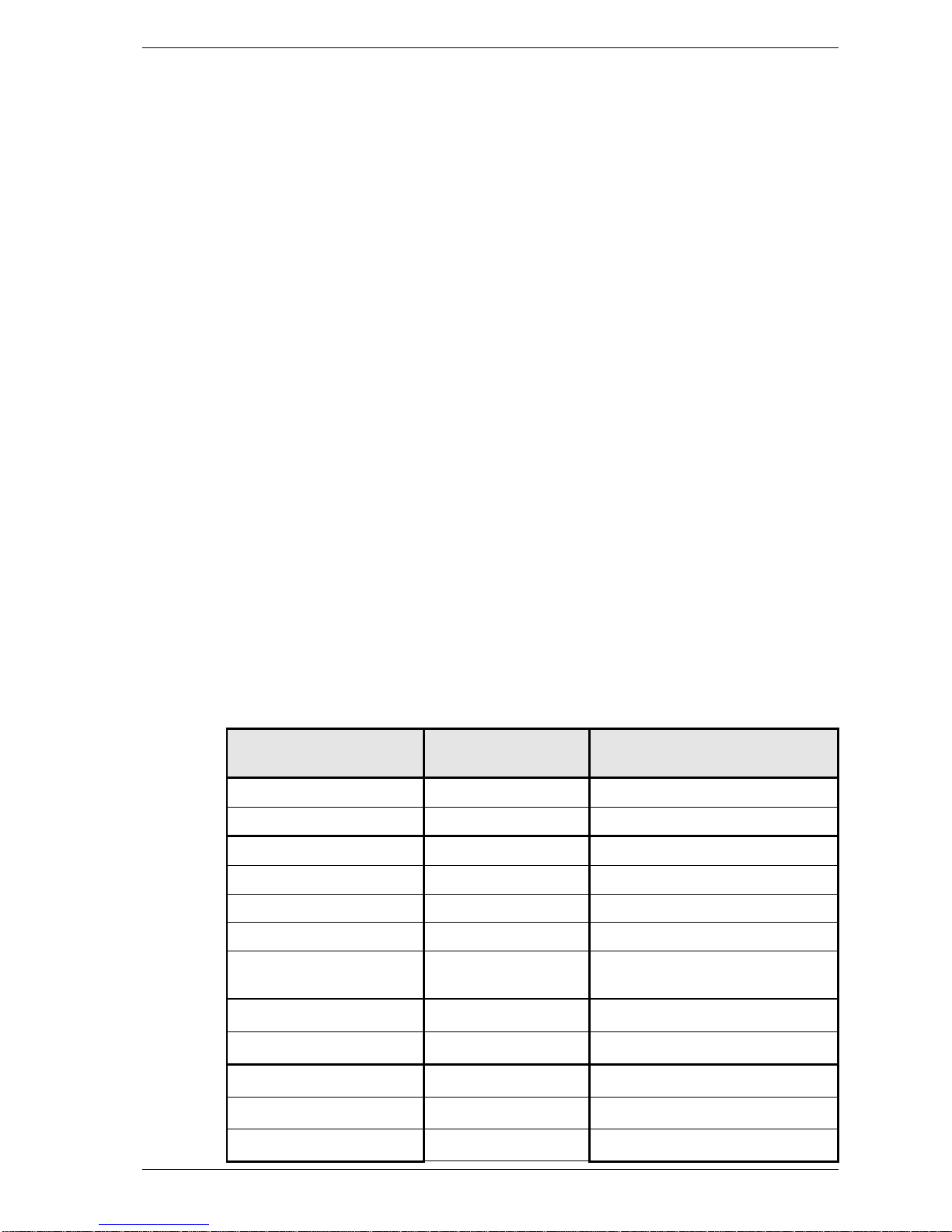
The sequence of operations performed during this routine are shown in table 3.
Event Signals of
interest
Comment
Set Green LED L5 on L5 CRO Synchronisation
Set Green LED L5 off L5 CRO Synchronisation
Move 01 to 40010004 IC16 pin 29 Write to RAM bank 0 byte 0
Move 02 to 40010005 IC17 pin 29 Write to RAM bank 0 byte 1
Move 04 to 40010006 IC18 pin 29 Write to RAM bank 0 byte 2
Move 08 to 40010007 IC19 pin 29 Write to RAM bank 0 byte 3
Move 40010004 to
CPU
IC16-19 pin 24 Read from RAM bank 0
Set Red LED L4 on L4 CRO Synchronisation
Set Red LED L4 off L4 CRO Synchronisation
Move 10 to 20000000 IC13 pin 29 Write to FLASH byte 0
Move 20 to 20000001 IC14 pin 29 Write to FLASH byte 1
Move 40 to 20000002 IC12 pin 29 Write to FLASH byte 2
Page 15
Boot ROM inbuilt Menu, sel f tests, setups , etc 5 - 3
Revision 1 - 07 July
1999 Event 4 TECHNICAL MANUAL
Move 80 to 20000003 IC11 pin 29 Write to FLASH byte 3
Move 20000004 to
CPU
IC11-14 pin 24 Read from FLASH
Move AA to 606A0000 IC65 pin 13 PC Memory Write
Move 606A0000 to
CPU
IC65 pin 14 PC Memory Read
Move 55 to 60000000 IC65 pin 50 PC IO Write
Move 60000000 to
CPU
IC65 pin 49 PC IO Read
Table 3: Bus exercise event summary
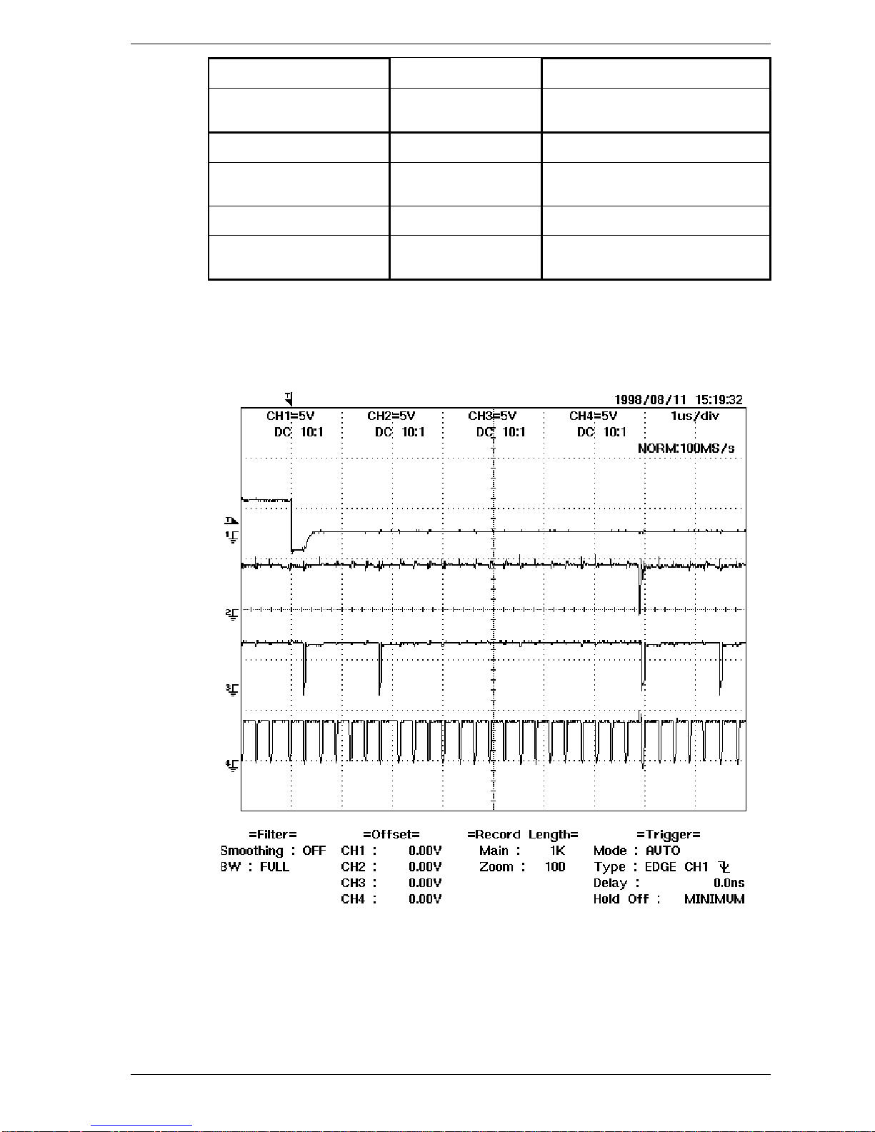
Figure 1 shows the relationship between L5, IC16 WR, and the CPU DACK signals as
measured while running this test.
Figure 1: Sample waveform during Bus Exercise
Trace #1: L5
Trace #2: IC16 Pin 29 (WR)
Trace #3: IC1 pin 44 (DACK1)
Trace #4: IC1 pin 43 (DACK0)
Page 16

Boot ROM inbuilt Menu, sel f tests, setups , etc 5 - 4
Revision 1 - 07 July
1999 Event 4 TECHNICAL MANUAL
RAM
The system RAM is checked for correct operation. This test requires approximately 2
minutes to execute.
FLASH
The system FLASH is checked for correct operation. This test requires approximately
50 seconds to execute. Note that due to the limited number of write cycles available in
FLASH devices, it is not recommended that this test be run continuously.
VGA
The VGA controller is initialised and a memory test is performed on its RAM. This
test takes approximately 17 seconds to execute and during execution a VGA monitor
will show the memory test patterns.
Ports
Use this option to test the ports of the CPU card. When selected the following options
are displayed:
1. VGA
2. DMX1
3. DMX2
4. MIDI
VGA
Test bars are displayed on the VGA and LCD screens for the purpose of checking
colour (VGA) and grey scaling (LCD). Press enter to return to the normal menu when
the screen results have been viewed.
DMX 1
The DMX1 output is connected to the MIDI input via the adaptor cable shown in
Appendix D, or the combiner circuit shown in Appendix E. When the test is run the
DMX1 output is exercised and the results read back into the MIDI input. The test takes
about 3 seconds to complete.
DMX 2
The DMX2 output is connected to the MIDI input via the adaptor cable shown in
Appendix D, or the combiner circuit shown in Appendix E. When the test is run the
DMX2 output is exercised and the results read back into the MIDI input. The test takes
about 3 seconds to complete.
Page 17

Boot ROM inbuilt Menu, sel f tests, setups , etc 5 - 5
Revision 1 - 07 July
1999 Event 4 TECHNICAL MANUAL
MIDI
The MIDI output is connected to the MIDI input via a standard MIDI link cable. When
the test is run the MIDI output is exercised and the results read back into the MIDI
input. The test takes about 3 seconds to complete.
Cards
Use this option to test the front panel cards of the console. When selected the
following options are displayed:
1. Scan
2. Activate
Scan
This test scans the front panel card bus and displays on the VDU the cards found.
When run continuously this test will activate the front panel card bus and the signals
can be used to troubleshoot faulty PCBs.
Activate
When run this test activates the front panel card bus as shown in Table 4, and can be
used to verify correct operation of the majority of the front panel controls. In general a
pressed switch is indicated by its associated LED (or the LCD if no LED available),
and fader values are displayed on the associated LCD or channel LED. The Channel
master levels and preset faders operate in familiar two preset mode, with the levels
appearing at both DMX outputs.
This test is terminated by pressing Exit.
Card Control Type Indication
Palette Palette select Associated LED
Assign Flash button Associated LED changes from
green to red
Assign Fader levels Associated LCD
Assign LCD contrast Controlled by Assign Fader #1
Master Buttons with red LED Associated LED
Master Buttons with Bicolour LED Associated LED turns from
green to red
Master Buttons with no LED LCD
Master Wheels LCD
Master Faders LCD
Preset Faders Associated Mimic LEDs
Preset Flash Buttons Associated Mimic LEDs
Table z: Front panel activation responses
Page 18

Boot ROM inbuilt Menu, sel f tests, setups , etc 5 - 6
Revision 1 - 07 July
1999 Event 4 TECHNICAL MANUAL
Misc
Use this option to run miscellaneous tests on the console. When selected the following
options are displayed:
1. DMX In
2. Vers
3. Trash RAM
DMX In
DMX signal from an external source is connected to the MIDI input using the adaptor
cable detailed in Appendix D. The DMX signal present is displayed on the VDU. Note
that both DMX outputs transmit a test data pattern that can be used to feed into the
input, however only one should be plugged into the MIDI input. Note also that the data
pattern changes each time the test is run.
Press Exit to terminate the test.
Vers
The software version of the test routines is output to L4 and L5 in flashes. The green
LED (L5) flashes once at the start of the test. The version is then displayed in red LED
(L4) flashes. The version is also displayed on the master LCD at startup, and for this
reason this test is mainly for use when no Master card is available.
Trash RAM
The system memory is completely cleared.
Boot
The console is restarted. This is generally used when use of the self tests has been
completed and it is desired to start the main operating software. Holding the Enter
button down immediately after activating this option allows re-entry to the self tests
and setups.
Page 19

Fault finding table 6 - 1
Revision 1 - 07 July
1999 Event 4 TECHNICAL MANUAL
6. Fault Finding Table
Symptom Possible Cause Remedy
Console won’t run
Show memory corrupt Deep Clear
Program memory corrupt Reload program
Mains fuse blown Replace fuse in power inlet
Front panel config error on start up
Flat cable disconnected Check that all flat cable connectors
are locked closed
Faulty flatcable Replace flatcable
Circuit board not working Replace card
Console crash with message
“Address error exception” etc
Software Bug Write down message and forward
to Jands, then try reboot or
program reload
Console drops its memory
Flat battery Replace battery
Power fail circuit out of adjustment Re-trim T1 as per section 3.1.2
Console always shows error
Software bug Write down message and forward
to Jands, then RAM trash as
described in section 5.3.3.4.3
Console won’t write or read diskette
Disk not DOS format Format on a PC compatible
computer (DOS 3.0 and above)
Diskette damaged Replace diskette
Poor quality diskette Use quality diskette
Diskette drive damaged Replace diskette drive
Fixture not available for patching
Fixture library in console not up to
date or corrupt
Load latest library from library
diskette.
No DMX output
Incorrect patch Check patch
Incorrect receiver address Check receiver
Faulty DMX cable Repair / replace cable
No line termination Terminate DMX line
Blown DMX driver Replace driver
Patch to other DMX output
Desk Lamp off
Short circuit lamp Remove short circuit then switch
console off for 1 minute
Level turned down Adjust level
Blown bulb Replace bulb
Radio Interference
Unearthed power cable Use earthed cable/outlet
Poor quality cables Use quality shielded cables
No intensity control from console
Grand Master down Adjust Grand Master
DMX
DBO button active Press DBO button
VGA monitor not working
Monitor not turned on Check power connection
Check power switch
Monitor not plugged into console Check VGA connection to console
Page 20

Maintenance 7 - 1
Revision 1 - 07 July
1999 Event 4 TECHNICAL MANUAL
7. Maintenance
If a console should start to misbehave or operate erratically, the problems encountered
can usually be attributed to one of two causes:
• normal wear and tear, eg. switches failing and becoming intermittent.
• physical abuse, eg. transit damage, spilt drinks, shorted cables.
Parts most likely to wear out in time with normal use include the following:
• switches
• faders
• LCD backlights
• digital encoders
These are generally easy to spot and there is little that can prevent such wear from
occurring, however careful use will maximise their life. Almost all parts of the console
can be damaged by physical abuse, however there are a number of things that can be
done to prevent this kind of damage:
• Cover the console when not in use, eg. before, after and between sets.
• ALWAYS insert a diskette into the floppy disk drive when the console is to be
transported. This prevents damage to the drive mechanism.
• Do not use spare audio lines for DMX cable. If so, there is a danger that the
connector will get plugged in to the wrong signal.
• Do not smoke over the console.
• Do not obstruct the rear ventilation holes.
• When cleaning, do not use solvents and never allow the entry of liquids into the
console. Use only a damp soft cloth for cleaning.
The console operating software is extremely complex. It is recommended that the
console be deep cleared at the start of each new tour.
Page 21

Technical Data and Specifications 8-1
Revision 1 - 07 July
1999 Event 4 TECHNICAL MANUAL
8. Technical Data and Specifications
Event 4 Specifications
Mains Supply: 90-265VAC, 47-63Hz, 60 watts max.
Mains Fuse: 2A, M205 delay type
Temperature: 40°C maximum ambient
Outputs: DMX Out 1 & 2, MIDI Thru, MIDI Out, Two Desk Lamps, VGA
Inputs: Keyboard (AT type), MIDI In
Control channels: 36 preset fader – 360, 24 preset fader - 240
Data Protocol: USITT DMX-512/1990, electrically conforms to RS485A.
Memory capacity: 2Mbytes
Disk Drive: IBM format DOS 3.0 and above, 1.44MB high density
Desk Lamps: 12 volt 5 watt x 2, maximum output 10W total
Construction: All steel chassis with lexan/polycarbonate covered control surface
Dimensions: L: 945mm W: 530mm H: 110mm
Weight: 19 kg net / 24.5 kg shipping
Ingress protection: IP20
Page 22

Glossary of Terms 9 - 1
Revision 1 - 07 July
1999 Event 4 TECHNICAL MANUAL
9. Glossary of Terms
Abbreviation Term Explanation
ADC Analogue to Digital
Converter
A device for converting real world (analog)
signals into digital information a micro-processor
can manipulate
BOOT BOOT System startup
CE Chip enable A select pin provided on a device to enable it to
be used in conjunction with a CS line
CE Compliance mark Equipment marked as such complies with the
European safety/EMC regulations
C-Tick Compliance mark Equipment marked as such complies with the
Australian EMC regulations
CPU Central Processing
Unit
The heart of a microprocessor or computer
CS Chip Select A connection that is asserted under certain
circumstances to select a particular device
DAC Digital to Analogue A device for generating an analogue
representation of a digital control signal
Converter
DIP Dual In-line
Package
A device package format with 2 parallel rows of
pins
EL Electroluminescent A type of backlight that uses high voltage
EPROM Erasable
Programmable
Read Only
Memory
A type of memory that is not intended to be reprogrammed in circuit
FLASH Flash RAM A type of memory very much like EPROM but
which is designed to be re-programmed insystem enabling program updates
GAL Generic Array
Logic
A logic device that can be programmed to
perform many logic functions
$ Hexadecimal
number
The number $A is 10
(decimal)
and $F is 15
(decimal)
IRQ Interrupt Request A connection that is asserted when a device has
information ready to be accessed by the CPU
Jumper Shunt, Link A jumper is used to configure a system by
shorting a pair of pins together
LED Light Emitting
Diode
A diode that is optimised to radiate light
LCD Liquid Crystal
Display
A type of display that uses a liquid to prevent the
transmission of light
NMI Non-Maskable
Interrupt
An IRQ that cannot be ignored
Page 23

Glossary of Terms 9 - 2
Revision 1 - 07 July
1999 Event 4 TECHNICAL MANUAL
PSU Power Supply Unit The power supply converts incoming mains to
voltages usable by the electronics
PWM Pulse Width
Modulation
A cyclic technique of digital power control where
a load is switched fully on for a period of time
dependant upon the required output power
RAM Random Access
Memory
Memory in which the data contained within can
be accessed in any order. The term RAM
generally refers to memory that can be read and
written to by the system
ROM Read Only
Memory
Memory that cannot be changed by the system
SMD Surface Mount
Device
A miniaturised leadless component mounted on
the upper or lower surface of a circuit board
SRAM Static RAM A form of RAM that uses static memory cells to
store information.
Page 24

Appendix A – History of M odi fications A - 1
Revision 1 - 07 July
1999 Event 4 TECHNICAL MANUAL
Appendix A: History of Modifications
Serial Number Modification
Page 25

Appendix B - Connector Pinouts B - 1
Revision 1 - 07 July
1999 Event 4 TECHNICAL MANUAL
Appendix B: Connector Pinouts
Front Panel Card Bus Connector (View from component side)
Palette, Assign, Master Cards
FDD Power Connector Main Power Connector (CONN8)
D0
GND
D3
D4
GND
D7
R/W
+5
MUX
+12
+5V
GND
GND
NC
GND
D1
D2
GND
D5
D6
+5
ALE
DS
-12
+5V
GND
-12V
GND
+5V
+12V
GND
DIM
Page 26

Appendix B - Connector Pinouts B - 2
Revision 1 - 07 July
1999 Event 4 TECHNICAL MANUAL
FDD Connector (CONN6) Expansion bus Connector (CONN2)
DMX CONNECTOR (Conn19)
DSKCHG
HDSEL
RDATA
WRTPRT
TRK0
WGATE
WDATA
STEP
DIR
MTR1
DS0
DS1
MTR0
INDEX
DRATE1
NC
DENSEL
GND
GND
GND
GND
GND
GND
GND
GND
GND
GND
GND
GND
GND
GND
GND
GND
GND
DMX1+
DMX1-
GND
DMX2-
DMX2+
GND
ACK
+12v
A2
A3
GND
A6
A7
GND
A10
A11
+5
A14
A15
GND
A18
IO
GND
R/W
D7
GND
D4
D3
GND
D0
INT
A0
A1
-12V
A4
A5
GND
A8
A9
GND
A12
A13
+5
A16
A17
GND
NC
RESET
GND
D6
D5
GND
D2
D1
GND
Page 27

Appendix B - Connector Pinouts B - 3
Revision 1 - 07 July
1999 Event 4 TECHNICAL MANUAL
DESK LAMP CONNECTIONS
PIN No. FUNCTION
1NC
2GND
3V+
DESK LAMP CONNECTOR
MIDI CONNECTIONS
PIN FUNCTION
No.
IN OUT THRU
1NCNCNC
2 NC SHIELD SHIELD
3NCNCNC
4 IN+ OUT+ OUT+
5 IN- OUT- OUT-
MIDI CONNECTOR
KEYBOARD CONNECTIONS
PIN No. FUNCTION
1KCLK
2KDATA
3NC
4GND
5+5V
KEYBOARD CONNECTOR
1
3
3
3
2
2
5
5
2
4
1
4
1
Page 28

Appendix B - Connector Pinouts B - 4
Revision 1 - 07 July
1999 Event 4 TECHNICAL MANUAL
DMX CONNECTIONS
PIN No. FUNCTION
1SHIELD
2SIGNAL-
3SIGNAL+
4NC
5NC
DMX CONNECTOR
VGA CONNECTIONS
PIN No. FUNCTION
1RED
2 GREEN
3BLUE
4NC
5NC
6 RED RETURN
7 GREEN RETURN
8 BLUE RETURN
9 NC
10 GND
11 NC
12 NC
13 HSYNC
14 VSYNC
15 NC
VGA CONNECTOR
5
3
4
1
11
6
2
1
Page 29

Appendix C - Spare Parts C - 1
Revision 1 - 07 July
1999 Event 4 TECHNICAL MANUAL
Appendix C: Spare Parts
The following spare parts for Event 4 consoles are available from the JANDS Service
Department:
ITEM PART No.
Switching power supply NFS40-7608 ZSX0200
Fuse M205 2 amp fast blow (mains) ZEF2150
3.5” Disk drive ZZA1440
Desklamp socket AXR-3-31PB ZPG0380
DMX out socket AXR-5-21PB ZPG2100
Fader 10K 60mm (Alps) ZRS0200
Fader knob black/white line ZZK0400
Fader knob black/blue line ZZK0450
Fader knob black/green line ZZK0460
Fader knob black/red line ZZK0470
Fader knob black/grey line ZZK0480
Encoder HRPG ZRP0450
Encoder knob ZZK1210
Switch (Schadow) SERU ZSW0450
Switchcap SRKL (Schadow) ZSC0050
Switch (Cherry) MX1A-A1NW ZSW1500
Switchcap (Cherry) no LED window ZSC0500
Switchcap (Cherry) with LED window ZSC0550
Lithium Battery 6126 CR (CPU) ZDC0100
75176 / DS3695 (DMX driver) ZIC1010
IC H11N1 ZIC0170
Small back light driver card complete YPC177
Preset Card complete YPC173
Palette card complete YPC172
Page 30

Appendix C - Spare Parts C - 2
Revision 1 - 07 July
1999 Event 4 TECHNICAL MANUAL
Assign card complete YPC175
Master card complete YPC176
CPU card complete YPC174
Page 31

Circuit Diagrams and Overlays D - 1
Revision 1 - 07 July
1999 Event 4 TECHNICAL MANUAL
R9
270R
IC2
75176
OPTO1
H11N1
8
5
7
6
2
1
5
4
6
IC1
75176
8
5
9
10
11
8
IC3C
74HC10
3
4
5
6
IC3B
74HC10
1
2
13
12
IC3A
74HC10
VCC
VCC
VCC
D1
1N914
R1
220R
VCC
VCC
VCC
R2
10K
R3
10K
R4
10K
R5
10K
VCC
1
2
3
From DM X1 output
1
2
3
From DM X2 output
4
5
From M IDI output
R6
220R
R7
220R
VCC
5
4
T o MID I I nput
VCC
5
4
From Keyboar d Input
C1
100nF
Appendix D: DMX to MIDI adaptor
A DMX to MIDI adaptor cable is required to run some of the Auxiliary tests contained in the Boot
ROM. The adaptor should be wired as shown:
DMX pin MIDI pin Detail
3 5 connect with 220R 0.25W 5% resistor
2 4 direct connection
1 2 direct connection
Appendix E: 2 x DMX, MIDI signal combiner
A DMX /MIDI combiner circuit is required to run some of the Auxiliary tests contained in the
Boot ROM.
Page 32

Circuit Diagrams and Overlays F - 1
Revision 1 - 07 July
1999 Event 4 TECHNICAL MANUAL
Appendix F: Circuit diagrams
Page 33

Circuit Diagrams and Overlays F - 2
Revision 1 - 07 July
1999 Event 4 TECHNICAL MANUAL
EV4CPU1 Circuit diagrams
Page 34

1 2 3 4 5 6 7 8
A
B
C
D
8
7654321
D
C
B
A
1
Jands Electronics P/L
40 Kent Rd
Mascot NSW 2020
Australia
Ph (02) 9582-0909
3
0
9-Jul-1999 16:34:10
H:\LAB\EVENT4\CIRCUIT\Ev4cpu1.sc1
Title
Size: Number:
Date:File:
Revision:
Sheet of
Time:
A2
Event4 CPU card
Ev4CPU1.SC1
Drawn By:
1. Set VR2 fully CCW
2. Short J1
3. Start Console
4. Adjust VR2 until L3 lights
5. Remove J1 short
R1
1K
C1
100nF
VCC
A/D81A/D92A/D103A/D114A/D125A/D138A/D149A/D1510A/D1611A/D1714A/D1815A/D1916A/D2017A/D2120A/D2221A/D2322A/D2423A/D2526A/D2627A/D2728A/D2829A/D2930A/D3033A/D31
34
TT035TT1
36
R/W
39
TS
40
SIZ0
41
SIZ1
42
DA0
43
DA1
44
DTIP
47
AA
48
BD49BR50BG
51
TBI
54
TEA
55
PST056PST157PST258PST3
59
AVEC
62
ATM
63
IPL064IPL165IPL2
66
RST
67
TRST/D
70
TDO/DSO
71
TDI/DSI
72
TMS/BKMT
73
TCK
74
HIZ
75
MTMOD076MTMOD177MTMOD2
78
DDATA081DDATA182DDATA283DDATA3
84
TIE LOW
85
CLK
87
A/D089A/D190A/D291A/D392A/D495A/D596A/D697A/D7
98
IC1
MCF5202
VCC
L1
LED GREEN
R2
1K
A02A13A24A35A46A57A68A7
9
B018B117B216B315B414B513B612B7
11
E
19
DIR
1
IC2
74HC245
A02A13A24A35A46A57A68A7
9
B018B117B216B315B414B513B612B7
11
E
19
DIR
1
IC3
74HC245
A02A13A24A35A46A57A68A7
9
B018B117B216B315B414B513B612B7
11
E
19
DIR
1
IC4
74HC245
A02A13A24A35A46A57A68A7
9
B018B117B216B315B414B513B612B7
11
E
19
DIR
1
IC5
74HC245
R3
1K
VCC
R4
1K
OC
1
CLK
11
1D22D33D44D55D66D77D88D
9
1Q192Q183Q174Q165Q156Q147Q138Q
12
IC6
74HC574
OC
1
CLK
11
1D22D33D44D55D66D77D88D
9
1Q192Q183Q174Q165Q156Q147Q138Q
12
IC7
74HC574
OC
1
CLK
11
1D22D33D44D55D66D77D88D
9
1Q192Q183Q174Q165Q156Q147Q138Q
12
IC8
74HC574
A02A13A24A35A46A57A68A7
9
B018B117B216B315B414B513B612B7
11
E
19
DIR
1
IC9
74HC245
A02A13A24A35A46A57A68A7
9
B018B117B216B315B414B513B612B7
11
E
19
DIR
1
IC10
74HC245
R27
10R
A012A111A210A39A48A57A66A75A827A9
26
A1023A1125A124A1328A1429A153A162A17
30
Vpp
1
D013D114D215D317D418D519D620D721CE22OE24WE
31
IC11
28020
A012A111A210A39A48A57A66A75A827A9
26
A1023A1125A124A1328A1429A153A162A17
30
Vpp
1
D013D114D215D317D418D519D620D721CE22OE24WE
31
IC12
28020
VR2
1K TRIM
C19
10uF
R5
1K
VCC
R28
10K
R29
4K7
VCC
R13
10K
L2
LED RED
Q2
BCX17
CEO12CEI13VOUT
2
VCC
3
VBATT
1
RES16WDI
11
GND
4
OSC17OSC2
8
LOW
6
PFI
9
PFO
10
BAT-ON
5
/RES
15
WDO
14
IC15
MAX693
VCC
BAT1
3V
VCC
C6
100nF
VCC
1234567
8
16151413121110
9
SW1
SW-DIP8
A012A111A210A39A48A57A66A75A827A9
26
A1023A1125A124A1328A143A1531A162A1730A18
1
D013D114D215D317D418D519D620D7
21
CE22OE24WE
29
GND
16
VSS
32
IC16
62040
A012A111A210A39A48A57A66A75A827A9
26
A1023A1125A124A1328A143A1531A162A1730A18
1
D013D114D215D317D418D519D620D7
21
CE22OE24WE
29
GND
16
VSS
32
IC17
62040
A012A111A210A39A48A57A66A75A827A9
26
A1023A1125A124A1328A143A1531A162A1730A18
1
D013D114D215D317D418D519D620D7
21
CE22OE24WE
29
GND
16
VSS
32
IC18
62040
A012A111A210A39A48A57A66A75A827A9
26
A1023A1125A124A1328A143A1531A162A1730A18
1
D013D114D215D317D418D519D620D7
21
CE22OE24WE
29
GND
16
VSS
32
IC19
62040
A02A13A24A35A46A57A68A7
9
B018B117B216B315B414B513B612B7
11
E
19
DIR
1
IC24
74HC245
A012A111A210A39A48A57A66A75A827A9
26
A1023A1125A124A1328A1429A153A162A17
30
Vpp
1
D013D114D215D317D418D519D620D721CE22OE24WE
31
IC13
28020
A012A111A210A39A48A57A66A75A827A9
26
A1023A1125A124A1328A1429A153A162A17
30
Vpp
1
D013D114D215D317D418D519D620D721CE22OE24WE
31
IC14
28020
A012A111A210A39A48A57A66A75A827A9
26
A1023A1125A124A13
28
CE/PGM
22
VCC
32
OE
24
GND
16
O013O114O215O317O418O519O620O7
21
VPP
1
A1429A153A162A1730A18
31
IC25
27020
A02A13A24A35A46A57A68A7
9
B018B117B216B315B414B513B612B7
11
E
19
DIR
1
IC26
74HC245
A02A13A24A35A46A57A68A7
9
B018B117B216B315B414B513B612B7
11
E
19
DIR
1
IC27
74HC245
A02A13A24A35A46A57A68A7
9
B018B117B216B315B414B513B612B7
11
E
19
DIR
1
IC28
74HC245
A02A13A24A35A46A57A68A7
9
B018B117B216B315B414B513B612B7
11
E
19
DIR
1
IC29
74HC245
R14
10K
R30
47K
L3
LED RED
R7
1K
VCC
OC
1
CLK
11
1D22D33D44D55D66D77D88D
9
1Q192Q183Q174Q165Q156Q147Q138Q
12
IC30
74HC574
VCC
R31
10R
R32
4M7
VCC
X1
32.768KHz
R34
470K
R8
1K
C25
10nF
R33
4M7
C26
22pF
D05D16D27D38D49D510D612D7
14
GND
15
CS16AS17DS21STBY20R/W19RESET
22
MOT
2
SQW
27
PS
26
CLKOUT
25
CLKFS
24
OSC13OSC2
4
IRQ
23
Vdd
28
NC
1
NC
11
NC
13
NC
18
IC31
MC146818A
VCC
R10
1K
R11
1K
VCC
ISP port
GND
INT
GND
Interface
BDM
DS
ALEH
ALEL
D6D2D1
D0
-12+5+5
+12
D5
D4D3D7
RW
GND
GND
GND
GND
GND
GND
GND
GND
GND
A4
A5
A6A7A10
A12
A14
A15A16
A18RWD7D3D4
D5
+12
+5
+5
-12
ACK
D0
D1D2D6
REsetIOA17
A13
A11
A9
A8A0A1
A2
A3
Card Bus
Expansion
Bus
GND
A0A1A2A3A4A5A6A7A8A9A10
A11
A12
A13
A14
A15
A16
A17
D24
D25
D26
D27
D28
D29
D30
D31
D24
D25
D26
D27
D28
D29
D30
D31
A2A3A4A5A6A7A8A9A10
A11
A12
A13
A14
A15
A16
A17
A18
A19
A2A3A4A5A6A7A8A9A10
A11
A12
A13
A14
A15
A16
A17
A18
A19
D24
D25
D26
D27
D28
D29
D30
D31
D16
D17
D18
D19
D20
D21
D22
D23
A2A3A4A5A6A7A8A9A10
A11
A12
A13
A14
A15
A16
A17
A18
A19
A2A3A4A5A6A7A8A9A10
A11
A12
A13
A14
A15
A16
A17
A18
A19
D16
D17
D18
D19
D20
D21
D22
D23
D8D9D10
D11
D12
D13
D14
D15
D8D9D10
D11
D12
D13
D14
D15
A2A3A4A5A6A7A8A9A10
A11
A12
A13
A14
A15
A16
A17
A18
A19
A2A3A4A5A6A7A8A9A10
A11
A12
A13
A14
A15
A16
A17
A18
A20A2A3A4A5A6A7A8A9
A10
A11
A12
A13
A14
A15
A16
A17
A18
A20
A2A3A4A5A6A7A8A9A10
A11
A12
A13
A14
A15
A16
A17
A18
A19
D0D1D2D3D4D5D6
D7
D0D1D2D3D4D5D6
D7
A24
A25
A26
A27
A28
A29
A30
A31
A0A1A2A3A4A5A6
A7
A8A9A10
A11
A12
A13
A14
A15
A16
A17
A18
A19
A20
A21
A22
A23
D0D1D2D3D4D5D6
D7
D8D9D10
D11
D12
D13
D14
D15
D16
D17
D18
D19
D20
D21
D22
D23
D24
D25
D26
D27
D28
D29
D30
D31
AD0
AD1
AD2
AD3
AD4
AD5
AD6
AD7
AD8
AD9
AD10
AD11
AD12
AD13
AD14
AD15
AD16
AD17
AD18
AD19
AD20
AD21
AD24
AD25
AD26
AD27
AD28
AD29
AD30
AD31
AD0
AD1
AD2
AD3
AD4
AD5
AD6
AD7
AD8
AD9
AD10
AD11
AD12
AD13
AD14
AD15
AD16
AD17
AD18
AD19
AD20
AD21
AD24
AD25
AD26
AD27
AD28
AD29
AD30
AD31
AD0
AD1
AD2
AD3
AD4
AD5
AD6
AD7
AD8
AD9
AD10
AD11
AD12
AD13
AD14
AD15
AD16
AD17
AD18
AD19
AD20
AD21
AD24
AD25
AD26
AD27
AD28
AD29
AD30
AD31
D24
D25
D26
D27
D28
D29
D30
D31
D24
D25
D26
D27
D28
D29
D30
D31
D24
D25
D26
D27
D28
D29
D30
D31
D24
D25
D26
D27
D28
D29
D30
D31
SRAMPOWR
C9
100nF
RESET
CLK24M
EXPINTIN
1
GND
2
Vcc
4
OUT
3
IC32
24MHz
R19
10K
R20
10K
R21
10K
R22
10K
R23
10K
R24
10K
R25
10K
R26
10K
EXPINTOUT
INTEN
KEYINT
DMXINT
MIDIINT
RS232INT
SRAMPOWR
A1
66
INTEN
9
A3
53
IPL0
2
DIPSW
4
SPAREOUT
5
D27
6
CARDDS
10
D2511D24
12
S1
13
MEMCLK
15
LA19
21
RS232INT
22
SIZ1
23
RAM1SIZ
24
BOOTROM
25
INT1
26
A20
27
A30
29
EXPACK
30
DA0
31
FLASHW3
34
FLASHRD
35
RAM2SIZ
36
MEM_WR
38
S2
39
A29
40
A9
41
EXPSEL
42
MEM_RD
43
VA9
44
LA9
45
INT5
52
SPAREIN
54
A31
55
S4
56
IO_WR
58
IO_RD
59
RAM1W0
60
FLASHW0
61
RAM1W2
62
FLASHW2
63
RAM2W367RAM2W268RAM2W1
69
ACLK
70
A0
71
RAM2W0
74
DA1
75
CPUCLK
83
MIDIINT
85
INT6
86
CARDBUF
87
RW
88
DMX2WR
89
IOCHRDY
90
A22
91
AA
92
IOSEL
94
A21
95
DMX1WR
96
DTIP
98
RAM1W3
99
RAM1W1
100
FLASHW1
101
A2
102
RAM1RD
103
CARDAL
104
RTCADD
105
RAM2RD
106
CARDMUX
107
TS
108
RTCDATA
117
S3
118
A4
119
D26
122
SIZ0
123
INT7
124
EXPINT
125
IPL2
126
IPL1
127
ALE
128
RESET
19
SDI20MODE
46
SDO50SCLK
78
ISPEN
18
MiscIO
121
CARDRW
3
IC33
2096
D24
D25
D26
SCLK
MODE
ISPEN
SDO
SDI
IOSEL
DMX1WR
DMX2WR
IORD
IOWR
MEMRD
MEMWR
ALE
IOCHRDY
SPAREOUT
SPAREIN
GND
GND
GND
GND
GND
SPARE
A0A1A2
A3A4A5A6A7A8A9
A10
A11
A12
A13
A14
A15
A16
A17
A18
GND
1
D02D13D25D36D48D59D611D712VCC
13
RW14ALE
15
VCC
16
DS17MUX18-1219+12
20
GND4GND7GND
10
CONN1
20WAYIDC
D02D13D25D36D48D59D611D7
12
A047A145A2
44
A342A441A539A638A736A835A933A10
32
A1130A1229A1327A1426A1524A1623A1721A18
20
INT49ACK
48
IO18SPARE17RESET15RW
14
CONN2
50WAYIDC
J1
LINK
REBOOT
LINK
CONN3
8X.1
JH2MAIN
1 2
3 4
5 6
7 8
9 10
11 12
13 14
15 16
17 18
19 20
21 22
23 24
25 26
CONN13
IDC26
A18
VCC
D(0..31)
A(0..31) R/W
A(0..31)
R78
2K2
R80
22K
R81
22K
R82
1K
VCC
R83
C108
R84
C109
R85
C110
R86
C111
R87
C112
R88
C113
R89
C114
R90
C115
R91
C116
R92
C117
R93
C118
R94
C119
-12
+12
VCC
R116
10K
VCC
VA9
C135
100nF
C136
100nF
R124
10K
R125
10K
R127
10K
VCC
C107
100nF
OC1CLK111D22D33D44D55D66D77D88D
9
1Q192Q183Q174Q165Q156Q147Q138Q
12
IC68
74HC574
L4
LED REDL5LED GREEN
R35
1K
R36
1K
D5
BAV103
R129
10K
R130
4K7
Backlite
R131
10K
VCC
D9
BAV103
D24
D25
D26
D27
D28
D29
D30
D31
A0
A1
A2
A3
A4
A9
A20
A21
A22
A29
A30
A31
Sys_Reset
NMI
AD22
AD23
AD22
AD23
AD22
AD23
C155
100nF
D6
BAV103
VCC
C12
10pF
VCC164882113
GND
1173349658197
112
VCC
7131925323846536069808894
100
GND
6121824313745526168798693
99
tp3
R18
1M
TP1
SHUNT
A20
Twelve x 220R Twelve x 10nF
A19
A19
Page 35

1 2 3 4 5 6 7 8
A
B
C
D
8
7654321
D
C
B
A
2
Jands Electronics P/L
40 Kent Rd
Mascot NSW 2020
Australia
Ph (02) 9582-0909
3
0
9-Jul-1999 16:35:55
H:\LAB\EVENT4\CIRCUIT\Ev4cpu1.sc2
Title
Size: Number:
Date:File:
Revision:
Sheet of
Time:
A2
Event4 CPU Card
Ev4CPU1.SC2
Drawn By:
1011
IC35E
74HC14
8 9
IC35D
74HC14
56
IC35C
74HC14
VCC
R39
0.47R 5W
L6
LED GREEN
R110
1K
+12
Q7
TIP42
R40
220R
Q5
BCX19
R43
10K
R51
47R
P1
RUE090
D3
BAV103D4BAV103
C10
100nF
C20
10uF
VCC
R521KR531KR541KR551KR56
1K
1
W2D7
3D34D25D16D07
XI8FF
9
Q010Q111Q213Q314Q8
15
R
18
Q419Q520Q621Q7
22
HF
23
EF
24
RS
25
FL
26
D628D529D430D3
31
12
17
27
IC38
7202
1
W2D7
3D34D25D16D07
XI8FF
9
Q010Q111Q213Q314Q8
15
R
18
Q419Q520Q621Q7
22
HF
23
EF
24
RS
25
FL
26
D628D529D430D3
31
12
17
27
IC39
7202
3 4
IC35B
74HC14
VCC VCC
R37
1K
R38
1K
VCC
R111
1K
VCC
DENSEL
1
MTR0
2
DS1
3
DS0
4
MTR1
5
Vss
6
DIR
7
STEP
8
WDATA
9
WGATE
10
HDSEL
11
INDEX
12
TRK0
13
WRTPRT
14
RDATA
16
DSKCHG
17
DRATE1
18
DRATE2
19
X1
20
Vcc
15
X2
21
IDED7
22
IDEENL
23
IDEENH
24
HDCS0
25
HDCS1
26
IOCS16
27
A0
28
A1
29
A2
30
A331A432A533A6
34
TC
35
DACK
36
SSPIRQ37PSPIRQ
38
PINTR39FINTR
40
A741A842A9
43
IOR
44
IOW45AEN
46
Vss
47
D048D149D2
50
D3
51
FDRQ
52
D4
53
D5
54
D6
55
D7
56
RESET
57
GAMECS
58
SLCT
59
PE
60
BUSY
61
ACK
62
PD7
63
PD6
64
PD5
65
PD4
66
Vss
67
PD3
68
PD2
69
PD1
70
PD0
71
Vcc
72
SLCTIN
73
INIT
74
ERROR
75
AUTOFD
76
STROBE
77
RXD1
78
TXD1
79
DSR1
80
RTS181CTS182DTR183RI184DCD185RI286DCD287RXD288TXD289DSR290RTS291CTS292DTR293DRV294Vss95MTR296DS397VIO98MTR399IOCHRD
100
IC48
37C665IR
VCC
1 2
IC35A
74HC14
123
4
5
6
7
8
IC50
75176
123
4
5
6
7
8
IC51
75176
VCC
VCC
VCC
VCC
R41
220R
R42
220R
R112
220R
R113
220R
VCC
D2
BAV103
VCC
R114
220R
R115
220R
R57
47R
R60
10R
R44
10K
R45
10K
C28
1uF
C29
1uF
B1
Bead
B2
Bead
B4
Bead
B3
Bead
VCC
VCC
PolySwitch
FDD
MIDI
KEYBOARD
DMX1
DMX2
In Thru Out
D24
D25
D26
D27
D28
D29
D30
D31
A0
A1
A2
A3A4A5
A6
A7A8A9
D(0..31)
A(0..31)
RESET
R/W
RSTDRV
D24
D25
D26
D27
D28
D29
D30
D31
D24
D25
D26
D27
D28
D29
D30
D31
A0
DMX1WR
DMX2WR
1
GND
2
Vcc
4
OUT
3
OSC1
24MHz
MIDIINT
RS232INT
IOWR
IORDCLK24M
IOCHRDY
1
2
3 4
5
6
IC52
H11N1
1 2
3 4
5 6
7 8
9 10
11 12
13 14
15 16
17 18
19 20
21 22
23 24
25 26
27 28
29 30
31 32
33 34
CONN6
34WAYIDC
A1
2
INTEN
3
A3
4
F12
10
F26
11
F2012F24
13
KEYB_CLK
15
SPAREOUT
21
F22
23
D2524D3125D27
26
F25
27
DMX1O
28
KEYB_DATA
29
RW
35
D26
36
VPP
38
DMXFULL
39
F28
40
SPAREIN
41
EXPINTIN
43
GLED
44
DMX2EMPTY
45
IO
53
PINTR
55
RLED
57
D28
59
F1660F17
61
DMX2RD
62
DMX1RD
63
F10
68
DMX2O
69
RES
70
MEMCLK
80
LAMPCLK
83
D3085D29
86
F11
87
F27
88
INT1
89
F23
90
DMX1FULL
91
A093A2
95
DMX1EMPTY
98
D24
99
LAMP
102
DMX1RESET
103
BACKLITE
105
DMX2RESET
106
EXPINTOUT
107
F21
108
KEYINT
117
F14
119
F15
121
F13
126
F18
127
SCLK
78
MODE46ISPEN
18
SDI
20
SDO
50
RESET
19
EnaVEE
123
VEE
125
Sys_Reset
6
LCDON
66
DISPOFF
8
NMI
54
DMX_Reset
128
IC53
2096
SPAREIN
SPAREOUT
SCLK
MODE
ISPEN
SDI
SDO
INTEN
KEYINT
DMXINT
EXPINTOUT
EXPINTIN
IOSEL
LAMPCLK
12345
CONN15
5PINDIN
1234567
8
CONN8
8X.156
VCC
VCC
+12
-12
12345
CONN16
5PINDIN
12345
CONN17
5PINDIN
12345
CONN18
5PINDIN
B6
Bead
B5
Bead
12345
CONN19
5X2MM
R48
1K
VCC
A0A1A2
A3
D24
D25
D26
D27
D28
D29
D30
D31
R108
1K
TH1
C870
TH2
C870
TH3
C870
TH4
C870
MOV2
SA12CA
MOV3
SA12CA
123
CONN7
3X.156
+12
B7
Bead
B8
Bead
B10
Bead
B9
Bead
B11
Bead
B12
Bead
Backlite
P2
KU3H
PolySwitch
Sys_Reset
NMI
123
4
CONN9
4X.156
+12
-12
VCC
AUX POWER
GND1173349658197112
VCC164882113
P3
RUE090
C165
100nF
MOV1
SA12CA
MOV4
SA12CA
Page 36

1 2 3 4 5 6 7 8
A
B
C
D
8
7654321
D
C
B
A
3
Jands Electronics P/L
40 Kent Rd
Mascot NSW 2020
Australia
Ph (02) 9582-0909
3
0
9-Jul-1999 16:37:12
H:\LAB\EVENT4\CIRCUIT\Ev4cpu1.sc3
Title
Size: Number:
Date:File:
Revision:
Sheet of
Time:
A2
Event4 CPU Card
Ev4CPU1.SC3
Drawn By:
1213
IC35F
74HC14
R62
10R
C13
100nF
R63
150R
R64
150R
C31
1uF
C14
100nF
C22
10uF
R58
47R
VCC
R70
150R
D8
BAV103
32
1
IC56
LM334
C34
220pF 1206
C35
220pF 1206
R71
47R
R72
47R
R59
47R
C23
10uF
C15
100nF
VCC
R73
1R
R74
1R
C32
1uF
R65
150R
R66
150R
C16
100nF
VCC
D01D1
2
WE
3
RAS
4
5
A06A17A28A39A411A512A613A714A8
15
OE
16
CAS
17
D218D3
19
IC57
414256
D01D1
2
WE
3
RAS
4
5
A06A17A28A39A411A512A613A714A8
15
OE
16
CAS
17
D218D3
19
IC58
414256
D01D1
2
WE
3
RAS
4
5
A06A17A28A39A411A512A613A714A8
15
OE
16
CAS
17
D218D3
19
IC59
414256
D01D1
2
WE
3
RAS
4
5
A06A17A28A39A411A512A613A714A8
15
OE
16
CAS
17
D218D3
19
IC60
414256
VDD1
1
EROM
2
SD15
3
SD14
4
SD13
5
SD12
6
VSS1
7
SD11
8
SD10
9
SD9
10
SD8
11
VSS2
12
MEMW
13
MEMR
14
LA17
15
LA18
16
LA19
17
LA20
18
LA21
19
LA22
20
LA23
21
IOCS16
22
MCS16
23
SHBE
24
BALE
25
VDD2
26
SA0
27
SA1
28
SA2
29
SA3
30
SA4
31
SA5
32
SA6
33
SA7
34
SA8
35
SA9
36
SA10
37
SA11
38
SA12
39
VSS3
40
RESET41SA1342SA1443SA1544SA1645AEN46IOCHRD47REFRESH48IOR49IOW500WS51IRQ52VSS453SD054SD155SD256SD357VDD358SD459SD560VSS561SD662SD763AVSS164VFILTR65AVDD166TWR67VSYNC68HSYNC69AVSS270OVRW71AVDD272EED173EECS74BLUE75GREEN76RED77IREF78P079VSS4
80
VDD4
81
P1
82
P2
83
P3
84
AVDD3
85
P4
86
P5
87
P6
88
P7
89
AVSSS3
90
VSS7
91
DCLK
92
BLANK
93
EVIDEO
94
ESYNC
95
EDCLK
96
MD31
97
MD30
98
MD29
99
MD28
100
VSS8
101
MD27
102
MD26
103
MD25
104
MD24
105
WE3
106
MD23
108
MD22
109
MD21
110
MD20
111
MD19
112
MD18
113
MD17
114
MD16
115
WE2
116
MD15
117
MD14
118
MD13
119
VSS9
120
VDD6
121
MD12
122
MD11
123
MD10
124
MD9
125
MD8
126
WE1
127
VSS10
128
MD7
129
MD6
130
MD5
131
MD4
132
MD3
133
MD2
134
MD1
135
MD0
136
VSS11
137
WE0
138
CAS
139
VDD7
140
OE
141
RAS
142
MA9
143
VSS12
144
MA8
145
MA7
146
MA6
147
MA5
148
MA4
149
MA3
150
MA2
151
MA1
152
MA0
153
AVDD4
154
MFILTR
155
AVSS4
156
MCLK
157
XTAL
158
OSC
159
VSS13
160
VDD5
107
IC65
GD5429
C36
10pF
R67
150R
R68
150R
R69
150R
C37
10pF
C38
10pF
C17
100nF
C24
10uF
C33
1uF
C18
100nF
R75
10R
R76
10R
Video
1
GND
2
Vcc
4
OUT
3
IC66
14.31818MHz
MD16
MD17
MD18
MD19
MD20
MD21
MD22
MD23
MD24
MD25
MD26
MD27
MD28
MD29
MD30
MD31
MA0
MA1
MA2
MA3
MA4
MA5
MA6
MA7
MA8
MA0
MA1
MA2
MA3
MA4
MA5
MA6
MA7
MA8
MA0
MA1
MA2
MA3
MA4
MA5
MA6
MA7
MA8
MA0
MA1
MA2
MA3
MA4
MA5
MA6
MA7
MA8
MD16
MD17
MD18
MD19
MD20
MD21
MD22
MD23
MD24
MD25
MD26
MD27
MD28
MD29
MD30
MD31
D24
D25
D26
D27
D28
D29
D30
D31
A0
A1
A2
A3
A4
A5
A6
A7
A8
A10
A11
A12
A13
A14
A15
A16
A17
A18
A19
A(0..31)
D(0..31)
ALE
MEMWR
MEMRD
RSTDRV
IOCHRDY
IOWR
IORD
123456789
1011121314
15
CONN11
VGACONN
MA0
MA1
MA2
MA3
MA4
MA5
MA6
MA7
MA8
C40
100nF
VCC
C41
100nF
VCC
C42
100nF
VCC
C43
100nF
VCC
C44
100nF
VCC
C46
100nF
VCC
C56
100nF
VCC
C57
100nF
VCC
C58
100nF
VCC
C59
100nF
VCC
C60
100nF
VCC
C61
100nF
VCC
C62
100nF
VCC
C63
100nF
VCC
C64
100nF
VCC
C65
100nF
VCC
C66
100nF
VCC
C68
100nF
VCC
C69
100nF
VCC
C70
100nF
VCC
C71
100nF
VCC
C72
100nF
VCC
C73
100nF
VCC
C74
100nF
VCC
C75
100nF
VCC
C76
100nF
VCC
C77
100nF
VCC
C78
100nF
VCC
C79
100nF
VCC
C80
100nF
VCC
C81
100nF
VCC
C82
100nF
VCC
C83
100nF
VCC
C84
100nF
VCC
C85
100nF
VCC
C86
100nF
VCC
C87
100nF
VCC
C88
100nF
VCC
C89
100nF
VCC
C90
100nF
VCC
C91
100nF
VCC
C92
100nF
VCC
C93
100nF
VCC
C94
100nF
VCC
C95
100nF
VCC
C96
100nF
VCC
C97
100nF
VCC
C98
100nF
VCC
C99
100nF
VCC
C100
100nF
VCC
C101
100nF
VCC
C102
100nF
VCC
C103
100nF
VCC
C104
100nF
VCC
C105
100nF
VCC
GND
1
D02D13D25D36D48D59D611D712VCC
13
RW14ALE
15
VCC
16
DS17MUX18-1219+12
20
GND4GND7GND
10
CONN4
20WAYIDC
R95
150R
C120
10nF
R96
150R
C121
10nF
R97
150R
C122
10nF
R98
150R
C123
10nF
R99
150R
C124
10nF
R100
150R
C125
10nF
R101
150R
C126
10nF
R102
150R
C127
10nF
R103
150R
C128
10nF
R104
150R
C129
10nF
R105
150R
C130
10nF
R106
150R
C131
10nF
F1
BEAD
F3
BEAD
F4
BEAD
F2
BEAD
VCC
+12
-12
C139
100nF
VCC
C140
100nF
VCC
C141
100nF
VCC
C142
100nF
VCC
VA9
C151
100nF
-12
C143
100nF
VCC
C150
10uF
-12
C152
100nF
+12
C153
10uF
+12
C145
10uF
-12
C147
10uF
+12
C148
100nF
+12
C144
220uF
VCC
C149
100nF
VCC
C154
100nF
VCC
C146
100nF
-12
R118
2R7
R117
2R7
R119
2R7
R17
2R7
R16
2R7
R15
2R7
Note: Either R73 OR R117, 118, 119 used
Note: Either R74 OR R15, 16, 17 used
Page 37

Circuit Diagrams and Overlays F - 3
Revision 1 - 07 July
1999 Event 4 TECHNICAL MANUAL
EV4MAST3 Circuit diagrams
Page 38

1 2 3 4 5 6 78
A
B
C
D
8
7654321
D
C
B
A
2
Jands Electronics P/L
40 Kent Rd
Mascot NSW 2020
Australia
Ph (02) 9582-0909
2
0
9-Jul-1999 16:37:42
H:\LAB\EVENT4\CIRCUIT\Ev4mast3.sc1
Title
Size: Number:
Date:File:
Revision:
Sheet of
Time:
A3
EVENT4 MASTER CARD
EV4MAST3
Drawn By:
R25
2K2
R24
1K
R9
2K2
89
IC22D
74HC14
1213
IC22F
74HC14
C44
10nF
C42
10nF
C40
10nF
A02A13A24A35A46A57A68A7
9
B018B117B216B315B414B513B612B7
11
E19DIR
1
IC25
74HC245
A02A13A24A35A46A57A68A7
9
B018B117B216B315B414B513B612B7
11
E19DIR
1
IC24
74HC245
12
IC22A
74HC14
10 11
IC22E
74HC14
56
IC22C
74HC14
3 4
IC22B
74HC14
P04P112P213P3
3
PE
1
CIN5U/D
10
CLK
15
RST
9
Q06Q111Q214Q32COUT
7
IC21
4516
P04P112P213P3
3
PE
1
CIN5U/D
10
CLK
15
RST
9
Q06Q111Q214Q32COUT
7
IC20
4516
P04P112P213P3
3
PE
1
CIN5U/D
10
CLK
15
RST
9
Q06Q111Q214Q32COUT
7
IC19
4516
R10
2K2
R11
2K2
R12
2K2
R13
2K2
R15
2K2
R8
4K7
R7
10K
R6
22K
R5
22K
R4
2K2
R3
4K7
-12
VCC
VCC
C24
100nF
R2
100R
A02A13A24A35A46A57A68A7
9
B018B117B216B315B414B513B612B7
11
E
19
DIR
1
IC1
74HC245
A02A13A24A35A46A57A68A7
9
B018B117B216B315B414B513B612B7
11
E19DIR
1
IC10
74HC245
A02A13A24A35A46A57A68A7
9
B018B117B216B315B414B513B612B7
11
E19DIR
1
IC11
74HC245
OC1CLK111D22D33D44D55D66D77D88D
9
1Q192Q183Q174Q165Q156Q147Q138Q
12
IC3
74HC574
OC1CLK111D22D33D44D55D66D77D88D
9
1Q192Q183Q174Q165Q156Q147Q138Q
12
IC2
74HC574
X013X114X215X312X41X55X62X74INH6A11B10C9VEE
7
X
3
IC6
4051
R1
100R
+12
-12
Vcc
20
Vin
1
INT
9
Vrf(-)
11
OFL
18
Vrf(+)
12
DB02DB13DB24DB3
5
CS
13
DB4
14
RD
8
DB5
15
WR/RDY
6
DB6
16
MODE
7
DB7
17
IC8
ADC0820
VCC
VCC
A
1
B
2
C
3
E1
4
E2
5
E3
6
Y0
15
Y1
14
Y2
13
Y3
12
Y4
11
Y5
10
Y6
9
Y7
7
IC5
74HC138
OC
1
C
11
1D22D33D44D55D66D77D88D
9
1Q192Q183Q174Q165Q156Q147Q138Q
12
IC23
74HC573
OC
1
C
11
1D22D33D44D55D66D77D88D
9
1Q192Q183Q174Q165Q156Q147Q138Q
12
IC13
74HC573
OC
1
C
11
1D22D33D44D55D66D77D88D
9
1Q192Q183Q174Q165Q156Q147Q138Q
12
IC12
74HC573
C6
10uF
A02A13A24A35A46A57A68A7
9
B018B117B216B315B414B513B612B7
11
E19DIR
1
IC4
74HC245
A02A13A24A35A46A57A68A7
9
B018B117B216B315B414B513B612B7
11
E19DIR
1
IC7
74HC245
A02A13A24A35A46A57A68A7
9
B018B117B216B315B414B513B612B7
11
E19DIR
1
IC14
74HC245
C4
10uF
R14
100K
VCC
VCC
VCC
VCC
R38
10K
R39
10K
R40
10K
R41
10K
R42
10K
R44
100K
R45
100K
R46
100K
R47
100K
R48
100K
R49
100K
C41
10nF
C43
10nF
C45
10nF
R43
10K
OC1C111D22D33D44D55D66D77D88D
9
1Q192Q183Q174Q165Q156Q147Q138Q
12
IC16
74HC573
VCC
R16
2K2
R18
22K
3
2
1
84
IC9A
TL072
5
6
7
IC9B
TL072
VCC
ID
SFT
GND
GND
GND
Card
CL
T5T4T3T2T1GP
CLBMFCFXSC
ct
TB
@TH&
NX
TBG
TBR
SCR
FIX
FCSBMCLR
GRP
CONTRAST
S/T
19
40 X 2
LCD1
LED6 LED7
+5
R/W
E
RS
GND
ALEL
R/W
DS
D1
D7D6D5D4
D3D2
D0
ALEH
-12
+5
+12
LED5
P1
P2ASHold
GM
Rate
Fixt
XT
54321RC0
+-><DBASHL
9
8
DBO
ASG
ASR
HDR
HDG
7654321
0
987
6
SW2 SW3 SW4 SW5 SW6
$8E$8D$8C$8B$8A
$8F$8E$8D
D0D1D2D3D4D5D6
D7
D0D1D2D3D4D5D6
D7
D0D1D2D3D4D5D6
D7
D0D1D2D3D4D5D6
D7
D0D1D2D3D4D5D6
D7D0
D1D2D3D4D5D6D7
D0D1D2D3D4D5D6
D7
D0D1D2D3D4D5D6
D7
D0D1D2D3D4D5D6
D7
DD0
DD1
DD2
DD3
DD4
DD5
DD6
DD7
DD0
DD1
DD2
DD3
DD4
DD5
DD6
DD7
DD0
DD1
DD2
DD3
DD4
DD5
DD6
DD7
S(1..37)
L(1..24)
F(1..7)
VSS
1
VCC
2
VO
3
RS
4
R/W
5
E
6
D07D18D29D310D411D512D613D7
14
LCD0A
LCD40X2
1516
LCD0B
LCD40X2
GND
1
D02D1
3
GND
4
D25D3
6
GND
7
D48D5
9
GND
10
D611D712VCC
13
RW14ALEH
15
VCC
16
DS17ALEL18-1219+12
20
CONN1
IDC20
vcc
-12
+12
GND1R/W2ALEH3ALEL4DEC5A36A27A18A09GND
10
DS
11
13141516171819
VCC
20
12
IC27
EV4GAL
GND1R/W2ALEH3ALEL4DEC5A36A27A18A09GND
10
DS
11
13141516171819
VCC
20
12
IC26
EV4GAL
/AW
/AR
LC0sp/BUS
EnL
EnH
DC
/L3
/L2
/L1S2S3S4S5
S6
D0D1D2D3D4D5D6
D7
D0D1D2D3D4D5D6
D7
D0D1D2D3D4D5D6
D7
D0D1D2D3D4D5D6
D7
D0D1D2D3D4D5D6
D7
L1L2L3L4L5L6L7
L8
L9
L10
L11
L12
L13
L14
L15
L16
L17
L18
L19
L20
L21
L22
L23
L24
R17
2K2
R19
2K2
R20
2K2
R21
2K2
R22
2K2
R23
2K2
R26
2K2
R27
2K2
R28
2K2
R29
2K2
R30
2K2
R31
2K2
R32
2K2
R33
2K2
R34
2K2
R35
2K2
R36
2K2
R37
2K2
VCC
3
c2d
4
GND
1
GND
5
ENC1
ENCODER
VCC
VCC
3
c2d
4
GND
1
GND
5
ENC2
ENCODER
VCC
3
c2d
4
GND
1
GND
5
ENC3
ENCODER
VCC
VCC
FADTOP
FADBOT
123
4
CONN2
4PIN
123
4
CONN3
4PIN
VR1
5K TRIM
F1F2F3F4F5F6F7
DAC
DD0
DD1
DD2
DD3
DD4
DD5
DD6
DD7
S1S2S3S4S5S6S7
S8
S9
S10
S11
S12
S13
S14
S15
S16
S17
S18
S19
S20
S21
S22
S23
S24
S25
S26
S27
S28
S29
S30
S31
S32
S33
S34
S35
S36
S37
R111
47K
R110
470K
R108
4K7
R109
10K
VCC
Page 39

1 2 3 4 5 6 78
A
B
C
D
8
7654321
D
C
B
A
3
Jands Electronics P/L
40 Kent Rd
Mascot NSW 2020
Australia
Ph (02) 9582-0909
3
0
9-Jul-1999 16:38:11
H:\LAB\EVENT4\CIRCUIT\Ev4mast3.sc2
Title
Size: Number:
Date:File:
Revision:
Sheet of
Time:
A3
EVENT4 MASTER CARD
EV4MAST3
Drawn By:
VCC
C1
10uF
C2
10uF
-12
C3
10uF
+12VCC VCC
C7
100nF
VCC
C8
100nF
VCC
C9
100nF
VCC
C10
100nF
VCC
C11
100nF
VCC
C12
100nF
VCC
C13
100nF
VCC
C14
100nF
VCC
C15
100nF
VCC
C16
100nF
VCC
C17
100nF
VCC
C18
100nF
VCC
C19
100nF
VCC
C20
100nF
VCC
C21
100nF
VCC
C22
100nF
VCC
C23
100nF
VCC
C25
100nF
VCC
C26
100nF
VCC
C27
100nF
VCC
C28
100nF
VCC
C29
100nF
VCC
C30
100nF
VCC
C31
100nF
F1
10K
C34
100nF
F2
10K
C35
100nF
F3
10K
C36
100nF
F4
10K
C37
100nF
F5
10K
C38
100nF
F6
10K
C39
100nF
F7
10K
C32
100nF
F(1..7)
FADTOP
FADBOT
R51
100K
S1A
Cherry
R52
100K
S2A
Cherry
R53
100K
S3A
Cherry
R54
100K
S4A
Cherry
R55
100K
S5A
Cherry
R56
100K
S6A
Cherry
R57
100K
S7A
Cherry
R58
100K
S8A
Cherry
R59
100K
S9A
Cherry
R60
100K
S10A
Cherry
R61
100K
S11A
Cherry
R62
100K
S12A
Cherry
R63
100K
S13A
Cherry
R64
100K
S14A
Cherry
R65
100K
S15A
Cherry
R86
100K
S16A
Cherry
R87
100K
S17A
Cherry
R88
100K
S18A
Cherry
R89
100K
S19A
Cherry
R90
100K
S20A
Cherry
R91
100K
S21A
Cherry
R92
100K
S22A
Cherry
R93
100K
S23A
Cherry
R94
100K
S24A
Cherry
R95
100K
S25A
Cherry
R96
100K
S26A
Cherry
R97
100K
S27A
Cherry
R98
100K
S28A
Cherry
R99
100K
S29A
Cherry
R100
100K
S30A
Cherry
R101
100K
S31A
Cherry
R102
100K
S32A
Cherry
R103
100K
S33A
Cherry
R104
100K
S34A
Cherry
R105
100K
S35A
Cherry
R106
100K
S36A
Cherry
R107
100K
S37A
Cherry
S2B
RED
R66
2K2
S6B
RED
R67
2K2
S4B
RED
R68
2K2
S5B
RED
R69
2K2
S9B
RED
R70
2K2
S7B
RED
R71
2K2
S8B
RED
R72
2K2
S12B
RED
R73
2K2
S24B
RED
R74
2K2
S10B
RED
R75
2K2
S11B
RED
R76
2K2
S30B
RED
R77
2K2
S31B
RED
R78
2K2
S32B
RED
R79
2K2
S25B
RED
R80
2K2
S26B
RED
R81
2K2
S27B
RED
R82
2K2
S28B
RED
R83
2K2
R
G
S22B
BICOLOUR
R84
1K
R
G
S21B
BICOLOUR
R85
1K
R
G
S23B
BICOLOUR
R50
1K
L1 L2 L3 L4 L5 L6 L7 L8 L9 L10 L11 L12 L13 L14 L15 L16 L17 L18
L19 L20 L21
L22 L23 L24
L(1..24)
S(1..37)
P1 P2 HOLD FIXT A/S GM RATE
F1 F2 F3 F4 F5 F6 F7
S1 S2 S3 S4S5 S6 S7S8 S9 S10S11 S12 S13 S14 S15
S16 S17S18 S19 S20
S21 S22 S23 S24
S25 S26 S27S28 S29 S30 S31 S32 S33 S34S35 S36 S37
12345
CONN4
5PIN
Page 40

Circuit Diagrams and Overlays F - 4
Revision 1 - 07 July
1999 Event 4 TECHNICAL MANUAL
EV4ASN3 Circuit diagrams
Page 41

1 2 3 4 5 6 78
A
B
C
D
8
7654321
D
C
B
A
2
Jands Electronics P/L
40 Kent Rd
Mascot NSW 2020
Australia
Ph (02) 9582-0909
3
0
20-Jul-1999
H:\LAB\EVENT4\CIRCUIT\Ev4asn3.sc1
Title
Size: Number:
Date:File:
Revision:
Sheet of
A3
EVENT4 ASSIGN CARD
EV4ASN3
Drawn By:
3
2
1
8 4
IC1A
TL072
5
6
7
IC1B
TL072
R1
2k2
R3
1K
R20
47K
VCC
R22
100k
OC1C111D22D33D44D55D66D77D88D
9
1Q192Q183Q174Q165Q156Q147Q138Q
12
IC2
74HC573
-12
R24
4K7
R2
2k2
R26
470K
R27
22K
R29
10K
R25
4K7
R30
2K2
R31
2K2
R32
2K2
R33
2K2
OC
1
C
11
1D22D33D44D55D66D77D88D
9
1Q192Q183Q174Q165Q156Q147Q138Q
12
IC3
74HC573
VCC
C1
100nF
R55
100R
A02A13A24A35A46A57A68A7
9
B018B117B216B315B414B513B612B7
11
E
19
DIR
1
IC4
74HC245
A02A13A24A35A46A57A68A7
9
B018B117B216B315B414B513B612B7
11
E19DIR
1
IC5
74HC245
A02A13A24A35A46A57A68A7
9
B018B117B216B315B414B513B612B7
11
E19DIR
1
IC6
74HC245
OC1CLK111D22D33D44D55D66D77D88D
9
1Q192Q183Q174Q165Q156Q147Q138Q
12
IC7
74HC574
OC1CLK111D22D33D44D55D66D77D88D
9
1Q192Q183Q174Q165Q156Q147Q138Q
12
IC8
74HC574
X013X114X215X312X41X55X62X74INH6A11B10C9VEE
7
X
3
IC9
4051
R56
100R
+12
-12
Vcc
20
Vin
1
INT
9
Vrf(-)
11
OFL
18
Vrf(+)
12
DB02DB13DB24DB3
5
CS
13
DB4
14
RD
8
DB5
15
WR/RDY
6
DB6
16
MODE
7
DB7
17
IC11
ADC0820
VCC
VCC
A1B2C3E14E25E3
6
Y015Y114Y213Y312Y411Y510Y69Y7
7
IC12
74HC138
OC
1
C
11
1D22D33D44D55D66D77D88D
9
1Q192Q183Q174Q165Q156Q147Q138Q
12
IC13
74HC573
VCC
VCC
C23
10uF
R23
100k
C24
10uF
VCC
S/T
19
(ML2261)
LED0 LED1
SW3 SW2
100-300VAC
TO BACKLIGHT
+5
SELECT
CARD
DATA BUS
CONTRAST
GND
ALEL
R/W
DS
D1
D7D6D5D4
D3D2
D0
ALEH
-12
+5
+12
123
487655
678
432
1
5678432
1
GND
GND
GND
1
4
VSS
1
VCC
2
VO
3
RS
4
R/W
5
E
6
D07D18D29D310D411D512D613D7
14
LCD1A
40X2 LCD
DD0
DD1
DD2
DD3
DD4
DD5
DD6
DD7
DD0
DD1
DD2
DD3
DD4
DD5
DD6
DD7
D0D1D2D3D4D5D6
D7
D0D1D2D3D4D5D6
D7L8
L1L2L3L4L5L6L7
LL8
LL1
LL2
LL3
LL4
LL5
LL6
LL7
D0D1D2D3D4D5D6
D7 D0
D1D2D3D4D5D6D7
D0D1D2D3D4D5D6
D7
S1S2S3S4S5S6S7
S8
D0D1D2D3D4D5D6
D7
F1F2F3F4F5F6F7
F8
S(1..8)
L(1..8) LL(1..8)
FADTOP
FADGND
F(1..8)
DD0
DD1
DD2
DD3
DD4
DD5
DD6
DD7
D0D1D2D3D4D5D6
D7
D0D1D2D3D4D5D6
D7
GND
1
D02D1
3
GND
4
D25D3
6
GND
7
D48D5
9
GND
10
D611D712VCC
13
RW14ALEH
15
VCC
16
DS17ALEL18-1219+12
20
CONN1
IDC20
DD0
DD1
DD2
DD3
DD4
DD5
DD6
DD7
R34
2K2
R35
2K2
R36
2K2
R37
2K2
R38
2K2
R39
2K2
R40
2K2
R41
2K2
R42
2K2
R43
2K2
R44
2K2
R45
2K2
R46
2K2
R47
2K2
R48
2K2
R49
2K2
R50
2K2
R51
2K2
R52
2K2
R53
2K2
R54
2K2
R21
10K
R28
4K7
R58
470K
R59
47K
VCC
X013X114X215X312X41X55X62X7
4
INH
6
A11B
10
C
9
VEE
7
X
3
IC10
4051
R57
100R
123
4
CONN2
4X.1
123
4
CONN3
4X.1
JP1
PINWAF8
vcc
+12
-12
RV1
5K
GND1R/W2ALEH3ALEL4DEC5A36A27A18A09GND
10
DS11AR
12
AW
13
BC
14
S315S2
16
LC0
17
L118L0
19
VCC
20
IC14 GAL16V8
Page 42

1 2 3 4
A
B
C
D
4
321
D
C
B
A
3
Jands Electronics P/L
40 Kent Rd
Mascot NSW 2020
Australia
Ph (02) 9582-0909
3
0
9-Jul-1999
H:\LAB\EVENT4\CIRCUIT\Ev4asn3.sc2
Title
Size: Number:
Date:File:
Revision:
Sheet of
A4
EVENT4 ASSIGN CARD
EV4ASN3
Drawn By:
C25
10uF
-12
C26
10uF
+12
C27
10uF
VCC
VCC
C2
100nF
VCC
C3
100nF
VCC
C4
100nF
VCC
C5
100nF
VCC
C6
100nF
VCC
C7
100nF
VCC
C8
100nF
VCC
C9
100nF
VCC
C10
100nF
VCC
C11
100nF
VCC
C12
100nF
VCC
C13
100nF
VCC
C14
100nF
C15
100nF
FADER1
10K
C16
100nF
FADER2
10K
C17
100nF
FADER3
10K
C18
100nF
FADER4
10K
C19
100nF
FADER5
10K
C20
100nF
FADER6
10K
C21
100nF
FADER7
10K
C22
100nF
FADER8
10K
F(1..8)
FADTOP
FADGND
L(1..8)
LL(1..8)
R4
1K
R5
1K
S1A
SERU
S1B
SERU1
R6
1K
R7
1K
S2A
SERU
S2B
SERU1
R8
1K
R9
1K
S3A
SERU
S3B
SERU1
R10
1K
R11
1K
S4A
SERU
S4B
SERU1
R12
1K
R13
1K
S5A
SERU
S5B
SERU1
R14
1K
R15
1K
S6A
SERU
S6B
SERU1
R16
1K
R17
1K
S7A
SERU
S7B
SERU1
R18
1K
R19
1K
S8A
SERU
S8B
SERU1
vcc
LL1 LL2 LL3 LL4 LL5 LL6 LL7 LL8
L1 L2 L3 L4 L5 L6 L7 L8
S(1..8)
S1 S2 S3 S4 S5 S6 S7 S8
F1 F2 F3 F4 F5 F6 F7 F8
-12
+12
C28
100nF
Page 43

Circuit Diagrams and Overlays F - 5
Revision 1 - 07 July
1999 Event 4 TECHNICAL MANUAL
EV4PRE3 Circuit diagrams
Page 44

1 2 3 4 5 6 78
A
B
C
D
8
7654321
D
C
B
A
2
Jands Electronics P/L
40 Kent Rd
Mascot NSW 2020
Australia
Ph (02) 9582-0909
3
0
9-Jul-1999 16:39:01
H:\LAB\EVENT4\CIRCUIT\Ev4pre3.sc1
Title
Size: Number:
Date:File:
Revision:
Sheet of
Time:
A3
EVENT4 PRESET CARD
EV4PRE3
Drawn By:
R1
R2
R3R4R5R6R7R8R9R10
R11
R12R13
R14
R15
R16
R17
R18 R19
R20
R21
R22
R23
R24 R25
C1
10uF
R26
100R
VCC
VCC
Vcc
20
Vin
1
INT
9
Vrf(-)
11
OFL
18
Vrf(+)
12
DB02DB13DB24DB3
5
CS
13
DB4
14
RD
8
DB5
15
WR/RDY
6
DB6
16
MODE
7
DB7
17
IC1
ADC0820
-12
+12
3
2
1
8 4
IC2A
TL072
5
6
7
IC2B
TL072
R27
100R
R28
100R
R29
100R
R30
100R
R31
100R
X013X114X215X312X41X55X62X74INH6A11B10C9VEE
7
X
3
IC3
4051
X013X114X215X312X41X55X62X74INH6A11B10C9VEE
7
X
3
IC4
4051
X013X114X215X312X41X55X62X74INH6A11B10C9VEE
7
X
3
IC5
4051
X013X114X215X312X41X55X62X74INH6A11B10C9VEE
7
X
3
IC6
4051
X013X114X215X312X41X55X62X74INH6A11B10C9VEE
7
X
3
IC7
4051
OC1CLK111D22D33D44D55D66D77D88D
9
1Q192Q183Q174Q165Q156Q147Q138Q
12
IC8
74HC574
OC1CLK111D22D33D44D55D66D77D88D
9
1Q192Q183Q174Q165Q156Q147Q138Q
12
IC9
74HC574
A02A13A24A35A46A57A68A7
9
B018B117B216B315B414B513B612B7
11
E19DIR
1
IC10
74HC245
A02A13A24A35A46A57A68A7
9
B018B117B216B315B414B513B612B7
11
E19DIR
1
IC11
74HC245
A02A13A24A35A46A57A68A7
9
B018B117B216B315B414B513B612B7
11
E
19
DIR
1
IC12
74HC245
A1B2C3E14E25E3
6
Y015Y114Y213Y312Y411Y510Y69Y7
7
IC13
74HC138
VCC
VCC
OC1C111D22D33D44D55D66D77D88D
9
1Q192Q183Q174Q165Q156Q147Q138Q
12
IC14
74HC573
C4
100nF
R32
100R
VCC
R34
100K
VCC
R33
100R
25 x 2K2
DATA BUS
D5
D6D7D1DS
R/W
ALEL
GND
+5
+12 -12
ALEH
+5
D0
D2D3
D4
A2A1A0 D1D0
GND
GND
GND
91011
12
1234567
8
1-1
1-2
2-1
4-2
4-1
3-2
3-1
2-2
8-2
8-1
7-2
7-1
6-2
6-1
5-2
5-1
12-2
12-1
11-2
11-1
10-2
10-1
9-2
9-1 1
8765432
121110
9
GND1R/W2ALEH3ALEL4DEC5A36A27A18A09GND
10
DS
11
DAC12ARD
13
14
AWR
15
S316S2
17
18
BUS19VCC
20
IC15
GAL16V8
D0D1D2D3D4D5D6
D7
D0D1D2D3D4D5D6
D7
D0D1D2D3D4D5D6
D7
D0D1D2D3D4D5D6
D7
D0D1D2D3D4D5D6
D7
DD0
DD1
DD2
DD3
DD4
DD5
DD6
DD7
DD0
DD1
DD2
DD3
DD4
DD5
DD6
DD7
DD0
DD1
DD2
DD3
DD4
DD5
DD6
DD7
S1S2S3S4S5S6S7
S8
S9
S10
S11
S12
F1F2F3F4F5F6F7
F8
F9
F10
F11
F12
F13
F14
F15
F16
F17
F18
F19
F20
F21
F22
F23
F24
L1L2L3L4L5L6L7
L8
L9
L10
L11
L12
F(1..24)
FADTOP
FADBOT
S(1..12)
L(1..12)
19
GND
1
D02D1
3
GND
4
D25D3
6
GND
7
D48D5
9
GND
10
D611D712VCC
13
RW14ALEH
15
VCC
16
DS17ALEL18-1219+12
20
CONN1
IDC20
CONN2
PINWAF8
DD0
DD1
DD2
DD3
DD4
DD5
DD6
DD7
CONN3
PINWAF8
-12
+12
VCC
1
8
VCC
R72
10K
R74
47K
R71
4k7
R73
470K
VCC
Page 45

1 2 3 4 5 6 78
A
B
C
D
8
7654321
D
C
B
A
3
Jands Electronics P/L
40 Kent Rd
Mascot NSW 2020
Australia
Ph (02) 9582-0909
3
0
9-Jul-1999
H:\LAB\EVENT4\CIRCUIT\Ev4pre3.sc2
Title
Size: Number:
Date:File:
Revision:
Sheet of
A3
EVENT4 PRESET CARD
EV4PRE3
Drawn By:
C2
10uF
C3
10uF
C5
100nF
VCC
C6
100nF
VCC
C7
100nF
VCC
C8
100nF
VCC
C9
100nF
VCC
C10
100nF
VCC
C11
100nF
VCC
C12
100nF
VCC
C13
100nF
VCC
C14
100nF
VCC
C15
100nF
VCC
C16
100nF
VCC
C17
100nF
VCC
C18
100nF
VCC
C19
100nF
VCC
C20
100nF
VCC
+12-12
S1A
SERU
VCC
R35
100K
S2A
SERU
VCC
R36
100K
S3A
SERU
VCC
R37
100K
S4A
SERU
VCC
R38
100K
S5A
SERU
VCC
R39
100K
S6A
SERU
VCC
R40
100K
S7A
SERU
VCC
R41
100K
S8A
SERU
VCC
R42
100K
S9A
SERU
VCC
R43
100K
S10A
SERU
VCC
R44
100K
S11A
SERU
VCC
R45
100K
S12A
SERU
VCC
R46
100K
R47
22k
C45
10nF
R59
4k7
S1B
3mm RED
-12
+12
3
2
1
411
IC16A
TL074
R48
22k
C46
10nF
R60
4k7
S2B
3mm RED
12
13
14
IC16D
TL074
R49
22k
C47
10nF
R61
4k7
S3B
3mm RED
10
9
8
IC16C
TL074
R50
22k
C48
10nF
R62
4k7
S4B
3mm RED
5
6
7
IC16B
TL074
R51
22k
C49
10nF
R63
4k7
S5B
3mm RED
-12
+12
3
2
1
411
IC17A
TL074
R52
22k
C50
10nF
R64
4k7
S6B
3mm RED
12
13
14
IC17D
TL074
R53
22k
C51
10nF
R65
4k7
S7B
3mm RED
10
9
8
IC17C
TL074
R54
22k
C52
10nF
R66
4k7
S8B
3mm RED
5
6
7
IC17B
TL074
R55
22k
C53
10nF
R67
4k7
S9B
3mm RED
-12
+12
3
2
1
411
IC18A
TL074
R56
22k
C54
10nF
R68
4k7
S10B
3mm RED
12
13
14
IC18D
TL074
R57
22k
C55
10nF
R69
4k7
S11B
3mm RED
10
9
8
IC18C
TL074
R58
22k
C56
10nF
R70
4k7
S12B
3mm RED
5
6
7
IC18B
TL074
L1
L2 L3
L4 L5
L6
L7
L8 L9
L10
L11 L12
S1 S2 S3 S4 S5 S6 S7 S8 S9 S10 S11 S12
S(1..12)
L(1..12)
C57
100nF
+12
-12
C58
100nF
+12
-12
C59
10uF
VCC
C21
100nF
F1
10K FADER
C22
100nF
F2
10K FADER
C23
100nF
F3
10K FADER
C24
100nF
F4
10K FADER
C25
100nF
F5
10K FADER
C26
100nF
F6
10K FADER
C27
100nF
F7
10K FADER
C28
100nF
F8
10K FADER
C29
100nF
F9
10K FADER
C30
100nF
F10
10K FADER
C31
100nF
F11
10K FADER
C32
100nF
F12
10K FADER
C33
100nF
F13
10K FADER
C34
100nF
F14
10K FADER
C35
100nF
F15
10K FADER
C36
100nF
F16
10K FADER
C37
100nF
F17
10K FADER
C38
100nF
F18
10K FADER
C39
100nF
F19
10K FADER
C40
100nF
F20
10K FADER
C41
100nF
F21
10K FADER
C42
100nF
F22
10K FADER
C43
100nF
F23
10K FADER
C44
100nF
F24
10K FADER
FADBOT
FADTOP
F(1..24)
F1 F2 F3 F4 F5 F6 F7 F8 F9 F10 F11 F12
F13 F14 F15 F16 F17 F18 F19 F20 F21 F22 F23 F24
Page 46

Circuit Diagrams and Overlays F - 6
Revision 1 - 07 July
1999 Event 4 TECHNICAL MANUAL
EV4PAL3 Circuit diagrams
Page 47

1 2 3 4 5 6 78
A
B
C
D
8
7654321
D
C
B
A
1
Jands Electronics P/L
40 Kent Rd
Mascot NSW 2020
Australia
Ph (02) 9582-0909
1
0
9-Jul-1999 16:38:37
H:\LAB\EVENT4\CIRCUIT\Ev4palt3.sc1
Title
Size: Number:
Date:File:
Revision:
Sheet of
Time:
A3
EVENT4 PALETTE CARD
EV4PALT3
Drawn By:
GND1R/W2ALEH3ALEL4DEC5A36A27A18A09GND
10
DS
11
S013S114S215L016L117L2
18
CS
19
VCC
20
12
IC4
GAL16V8
VCC
C11
10uF
A02A13A24A35A46A57A68A7
9
B018B117B216B315B414B513B612B7
11
E19DIR
1
IC2
74HC245
R41
100k
VCC
C12
10uF
OC
1
C
11
1D22D33D44D55D66D77D88D
9
1Q192Q183Q174Q165Q156Q147Q138Q
12
IC7
74HC573
VCC
OC
1
C
11
1D22D33D44D55D66D77D88D
9
1Q192Q183Q174Q165Q156Q147Q138Q
12
IC12
74HC573
A1B2C3E14E25E3
6
Y015Y114Y213Y312Y411Y510Y69Y7
7
IC5
74HC138
VCC
OC1CLK111D22D33D44D55D66D77D88D
9
1Q192Q183Q174Q165Q156Q147Q138Q
12
IC3
74HC574
A02A13A24A35A46A57A68A7
9
B018B117B216B315B414B513B612B7
11
E19DIR
1
IC11
74HC245
A02A13A24A35A46A57A68A7
9
B018B117B216B315B414B513B612B7
11
E19DIR
1
IC10
74HC245
A02A13A24A35A46A57A68A7
9
B018B117B216B315B414B513B612B7
11
E
19
DIR
1
IC1
74HC245
S10A
VCC
R10
100K
OC
1
C
11
1D22D33D44D55D66D77D88D
9
1Q192Q183Q174Q165Q156Q147Q138Q
12
IC13
74HC573
5
10
15
20
3
8
13
18
4
9
14
19
1
6
11
16
2
7
12
17
20
15
10
5
19
14
9
4
18
13
8
3
17
12
7
2
16
11
6
1
$9D$9E$9F
$9F $9E $9D
GND
1
D02D1
3
GND
4
D25D3
6
GND
7
D48D5
9
GND
10
D611D7
12
VCC
13
RW
14
ALEH
15
VCC
16
DS
17
ALEL
18
-12
19
+12
20
CONN1
20WAY LATCH HEADER
DD0
DD1
DD2
DD3
DD4
DD5
DD6
DD7
+12
-12
VCC
S1A
R1
100K
S2A
R2
100K
S3A
R3
100K
S4A
R4
100K
S5A
R5
100K
S6A
R6
100K
S7A
R7
100K
S8A
R8
100K
S9A
R9
100K
S1
S2
S3
S4
S5
S6
S7
S8
S9
S10
S20A
VCC
R20
100K
S11A
R11
100K
S12A
R12
100K
S13A
R13
100K
S14A
R14
100K
S15A
R15
100K
S16A
R16
100K
S17A
R17
100K
S18A
R18
100K
S19A
R19
100K
S11
S12
S13
S14
S15
S16
S17
S18
S19
S20
R21
2k2
S1B
LED
R22
2k2
S2B
LED
R23
2k2
S3B
LED
R24
2k2
S4B
LED
R25
2k2
S5B
LED
R26
2k2
S6B
LED
R27
2k2
S7B
LED
R28
2k2
S8B
LED
R29
2k2
S9B
LED
R30
2k2
S10B
LED
R31
2k2
S11B
LED
R32
2k2
S12B
LED
R33
2k2
S13B
LED
R34
2k2
S14B
LED
R35
2k2
S15B
LED
R36
2k2
S16B
LED
R37
2k2
S17B
LED
R38
2k2
S18B
LED
R39
2k2
S19B
LED
R40
2k2
S20B
LED
C1
100nF
VCC
C2
100nF
VCC
C3
100nF
VCC
C4
100nF
VCC
C5
100nF
VCC
C6
100nF
VCC
C7
100nF
VCC
C8
100nF
VCC
C9
100nF
VCC
C10
100nF
VCC
L1 L2 L3 L4 L5 L6 L7 L8 L9 L10
L11 L12 L13 L14 L15 L16 L17 L18 L19 L20
S1S2S3S4S5S6S7
S8
S9
S10
S11
S12
S13
S14
S15
S16
S17
S18
S19
S20
S(1..20)
D0D1D2D3D4D5D6
D7
D0D1D2D3D4D5D6
D7
D0D1D2D3D4D5D6
D7
DD0
DD1
DD2
DD3
DD4
DD5
DD6
DD7
DD0
DD1
DD2
DD3
DD4
DD5
DD6
DD7
D0D1D2D3D4D5D6
D7
D0D1D2D3D4D5D6
D7
D0D1D2D3D4D5D6
D7
D0D1D2D3D4D5D6
D7
L1L2L3L4L5L6L7
L8
L9
L10
L11
L12
L13
L14
L15
L16
L17
L18
L19
L20
L(1..20)
S(1..20)
L(1..20)
Page 48

Circuit Diagrams and Overlays F - 7
Revision 1 - 07 July
1999 Event 4 TECHNICAL MANUAL
BKLTSML2 Circuit diagrams
Page 49

1 2 3 4
A
B
C
D
4
321
D
C
B
A
1
Jands Electronics P/L
40 Kent Rd
Mascot NSW 2020
Australia
Ph (02) 9582-0909
1
0
9-Jul-1999
H:\LAB\EVENT4\CIRCUIT\Bkltsml2.sch
Title
Size: Number:
Date:File:
Revision:
Sheet of
A4
Small Backlight driver
bkltsml0
Drawn By:
R1
100R
R2
100R
C1
10uF
+12
C2
10uF
-12
R3
10k
+12
R4
220R
Q1
BCX17
Q2
BCX19
R5
10k
+12
100-300VAC
TO BACKLIGHT
INV1
Seiko 5C
T1p
U1p
Output 1
Output 2
 Loading...