

Page 1

Distributed by:
www.Jameco.com ✦ 1-800-831-4242
The content and copyrights of the attached
material are the property of its owner.
Page 2
®
Rabbit 3000® Microprocessor
User’s Manual
019–0108 • 040731–O
Page 3

Rabbit 3000 Microprocessor User’s Manual
Part Number 019-0108 • 040731–O • Printed in U .S.A.
©2002–2004 Rabbit Semiconductor • All rights reserved.
Rabbit Semiconductor reserves the right to make changes and
improvements to its products without providing n otice.
T r ade mark s
Rabbit and Rabbit 3000 are registered trademarks of Rabbit Semi conduct or.
Dynamic C is a registered trademark of Z-World, Inc.
Rabbit Semiconductor
2932 Spafford S treet
Davis, California 95616-6800
USA
Telephone: (530) 757-8400
Fax: (530) 757-8402
www.rabbitsemiconductor.com
Rabbit 3000 Microprocessor
Page 4

TABLE OF CONTENTS
Chapter 1. Introduction 1
1.1 Features and Specifications Rabbit 3000..............................................................................................2
1.2 Summary of Rabbit 3000 Advantages..................................................................................................6
1.3 Differences Rabbit 3000 vs. Rabbit 2000.............................................................................................7
Chapter 2. Rabbit 3000 Design Features 9
2.1 The Rabbit 8-bit Processor vs. Other Processors................................................................................10
2.2 Overview of On-Chip Peripherals and Features.................................................................................11
2.2.1 5 V Tolerant Inputs .............................. ...... .................................. ..... ...... ...................................11
2.2.2 Serial Ports .................................................................................................................................11
2.2.3 System Clock .............................................................................................................................12
2.2.4 32.768 kHz Oscillator Input .......................................................................................................12
2.2.5 Parallel I/O .................................................................................................................................13
2.2.6 Slave Port ...................................................................................................................................14
2.2.7 Auxiliary I/O Bus .......................................................................................................................15
2.2.8 Timers ........................................................................................................................................15
2.2.9 Input Capture Channels ..............................................................................................................16
2.2.10 Quadrature Encoder Inputs ......................................................................................................17
2.2.11 Pulse Width Modulation Outputs .............................................................................................17
2.2.12 Spread Spectrum Clock ............................................................................................................18
2.2.13 Separate Core and I/O Power Pins ...........................................................................................18
2.3 Design Standards................................................................................................................................18
2.3.1 Programming Port ......................................................................................................................18
2.3.2 Standard BIOS ...........................................................................................................................19
2.4 Dynamic C Support for the Rabbit.....................................................................................................19
Chapter 3. Details on Rabbit Microprocessor Features 21
3.1 Processor Registers.............................................................................................................................21
3.2 Memory Mapping...............................................................................................................................23
3.2.1 Extended Code Space .................................................................................................................26
3.2.2 Separate I and D Space - Extending Data Memory ...................................................................27
3.2.3 Using the Stack Segment for Data Storage ................................................................................29
3.2.4 Practical Memory Considerations ..............................................................................................30
3.3 Instruction Set Outline........................................................................................................................32
3.3.1 Load Immediate Data to a Register ............................................................................................33
3.3.2 Load or Store Data from or to a Constant Address ....................................................................33
3.3.3 Load or Store Data Using an Index Register .............................................................................34
3.3.4 Register-to-Register Move .........................................................................................................35
3.3.5 Register Exchanges ....................................................................................................................35
3.3.6 Push and Pop Instructions ..........................................................................................................36
3.3.7 16-bit Arithmetic and Logical Ops ............................................................................................36
3.3.8 Input/Output Instructions ...........................................................................................................39
3.4 How to Do It in Assembly Language—Tips and Tricks....................................................................40
3.4.1 Zero HL in 4 Clocks ...................................................................................................................40
3.4.2 Exchanges Not Directly Implemented .......................................................................................40
3.4.3 Manipulation of Boolean Variables ...........................................................................................40
3.4.4 Comparisons of Integers ............................................................................................................41
3.4.5 Atomic Moves from Memory to I/O Space ...............................................................................43
User’s Manual
Page 5

3.5 Interrupt Structure..............................................................................................................................44
3.5.1 Interrupt Priority ........................................................................................................................ 44
3.5.2 Multiple External Interrupting Devices .....................................................................................46
3.5.3 Privileged Instructions, Critical Sections and Semaphores ....................................................... 46
3.5.4 Critical Sections ......................................................................................................................... 47
3.5.5 Semaphores Using Bit B,(HL) ..................................................................................................47
3.5.6 Computed Long Calls and Jumps ..............................................................................................48
Chapter 4. Rabbit Capabilities 49
4.1 Precisely Timed Output Pulses ..........................................................................................................49
4.1.1 Pulse Width Modulation to Reduce Relay Power .....................................................................50
4.2 Open-Drain Outputs Used for Key Scan............................................................................................51
4.3 Cold Boot...........................................................................................................................................52
4.4 The Slave Port....................................................................................................................................53
4.4.1 Slave Rabbit As A Protocol UART ...........................................................................................54
Chapter 5. Pin Assignments and Functions 55
5.1 LQFP Package....................................................................................................................................56
5.1.1 Pinout .........................................................................................................................................56
5.1.2 Mechanical Dimensions and Land Pattern ................................................................................57
5.2 Ball Grid Array Package...................................................................................................................59
5.2.1 Pinout .........................................................................................................................................59
5.2.2 Mechanical Dimensions and Land Pattern ................................................................................60
5.3 Rabbit Pin Descriptions......................................................................................................................62
5.4 Bus Timing.........................................................................................................................................64
5.5 Description of Pins with Alternate Functions....................................................................................65
5.6 DC Characteristics..............................................................................................................................68
5.7 I/O Buffer Sourcing and Sinking Limit..............................................................................................69
Chapter 6. Rabbit Internal I/O Registers 71
6.1 Default Values for all the Peripheral Contro l Registers..................... ................................................73
Chapter 7. Miscellaneous Functions 79
7.1 Processor Identification......................................................................................................................79
7.2 Rabbit Oscillators and Clocks............................................................................................................80
7.3 Clock Doubler....................................................................................................................................83
7.4 Clock Spectrum Spreader...................................................................................................................86
7.5 Chip Select Options for Low Power ..................................................................................................87
7.6 Output Pins CLK, STATUS, /WDTOUT, /BUFEN..........................................................................90
7.7 Time/Date Clock (Real-Time Clock).................................................................................................91
7.8 Watchdog Timer.................................................................................................................................93
7.9 System Reset......................................................................................................................................95
7.10 Rabbit Interrupt Structure.................................................................................................................97
7.10.1 External Interrupts ...................................................................................................................99
7.10.2 Interrupt Vectors: INT0 - EIR,0x00/INT1 - EIR,0x08 ..........................................................100
7.11 Bootstrap Operation.......................................................................................................................101
7.12 Pulse Width Modulator ....................................... ...... .....................................................................103
7.13 Input Capture..................................................................................................................................105
7.14 Quadrature Decoder.......................................................................................................................110
Chapter 8. Memory Interface and Mapping 115
8.1 Interface for Static Memory Chips...................................................................................................115
8.2 Memory Mapping Overview............................................................................................................117
8.3 Memory-Mapping Unit....................................................................................................................117
8.4 Memory Interface Unit.....................................................................................................................119
Rabbit 3000 Microprocessor
Page 6

8.5 Memory Bank Control Registers......................................................................................................120
8.5.1 Optional A16, A19 Inversions by Segment (/CS1 Enable) .....................................................121
8.6 Allocation of Extended Code and Data............................................................................................123
8.7 Instruction and Data Space Support..................................................................................................124
8.8 How the Compiler Compiles to Memory .........................................................................................127
Chapter 9. Parallel Ports 129
9.1 Parallel Port A...................................................................................................................................130
9.2 Parallel Port B...................................................................................................................................131
9.3 Parallel Port C...................................................................................................................................132
9.4 Parallel Port D...................................................................................................................................133
9.5 Parallel Port E...................................................................................................................................137
9.6 Parallel Port F ...................................................................................................................................140
9.6.1 Using Parallel Port A and Parallel Port F ................................................................................141
9.7 Parallel Port G...................................................................................................................................143
Chapter 10. I/O Bank Control Registers 145
Chapter 1 1. Timers 149
11.1 Timer A...........................................................................................................................................150
11.1.1 Timer A I/O Registers ............................................................................................................151
11.1.2 Practical Use of Timer A .......................................................................................................155
11.2 Timer B...........................................................................................................................................156
11.2.1 Using Timer B ........................................................................................................................159
Chapter 12. Rabbit Serial Ports 161
12.1 Serial Port Register Layout..................................................... ...... ...... ............................................164
12.2 Serial Port Registers.......................................... ..... .........................................................................166
12.3 Serial Port Interrupt ............................................... ...... ...... .............................................................179
12.4 Transmit Serial Data Timing ..........................................................................................................180
12.5 Receive Serial Data Timing............................................................................................................181
12.6 Clocked Serial Ports........................................................................................................................182
12.7 Clocked Serial Timing....................................................................................................................185
12.7.1 Clocked Serial Timing With Internal Clock ..........................................................................185
12.7.2 Clocked Serial Timing with External Clock ..........................................................................185
12.8 Synchronous Communications on Ports E and F............................................................................187
12.9 Serial Port Software Suggestions....................................................................................................192
12.9.1 Controlling an RS-485 Driver and Receiver ..........................................................................193
12.9.2 Transmitting Dummy Characters ...........................................................................................193
12.9.3 Transmitting and Detecting a Break ......................................................................................194
12.9.4 Using A Serial Port to Generate a Periodic Interrupt .............................................................194
12.9.5 Extra Stop Bits, Sending Parity, 9th Bit Communication Schemes .......................................194
12.9.6 Parity, Extra Stop Bits with 7-Data-Bit Characters ...............................................................195
12.9.7 Parity, Extra Stop Bits with 8-Data-Bit Characters ...............................................................195
12.9.8 Supporting 9th Bit Communication Protocols .......................................................................196
12.9.9 Rabbit-Only Master/Slave Protocol .......................................................................................196
12.9.10 Data Framing/Modbus .............................................................................................. ...........196
Chapter 13. Rabbit Slave Port 199
13.1 Hardware Design of Slave Port Interconnection ............................................................................204
13.2 Slave Port Registers........................................................................................................................204
13.3 Applications and Communications Proto cols for Slaves................................................................206
13.3.1 Slave Applications .................................................................................................................206
13.3.2 Master-Slave Messaging Protocol .........................................................................................207
User’s Manual
Page 7

Chapter 14. Rabbit 3000 Clocks 209
14.1 Low-Power Design.........................................................................................................................210
Chapter 15. EMI Control 211
15.1 Power Supply Connections and Board Layout ..............................................................................2 12
15.2 Using the Clock Spectrum Spreader..............................................................................................212
Chapter 16. AC Timing Specifications 215
16.1 Memory Access Time.................................................................................................................... 215
16.2 I/O Access Time.............................................................................................................................223
16.3 Further Discussion of Bus and Clock Timing................................................................................225
16.4 Maximum Clock Speeds................................................................................................................227
16.5 Power and Current Consumption...................................................................................................2 29
16.6 Current Consumption Mechanisms..................... .................................. ...... ...... .............................232
16.7 Sleepy Mode Current Consumption...............................................................................................233
16.8 Memory Current Consumption ......................................................................................................234
16.9 Battery-Backed Clock Current Consumption ................................................................................235
16.10 Reduced-Power External Main Oscillator....................................................................................236
Chapter 17. Rabbit BIOS and Virtual Driver 237
17.1 The BIOS........................................................................................................................................237
17.1.1 BIOS Services .......................................................................................................................237
17.1.2 BIOS Assumptions ................................................................................................................238
17.2 Virtual Driver.................................................................................................................................238
17.2.1 Periodic Interrupt ...................................................................................................................238
17.2.2 Watchdog Timer Support ......................................................................................................238
Chapter 18. Other Rabbit Software 241
18.1 Power Management Support..........................................................................................................241
18.2 Reading and Writing I/O Registers................................................................................................ 242
18.2.1 Using Assembly Language ....................................................................................................242
18.2.2 Using Library Functions ........................................................................................................242
18.3 Shadow Registers...................................................... ...... ...............................................................243
18.3.1 Updating Shadow Registers ..................................................................................................243
18.3.2 Interrupt While Updating Registers .......................................................................................243
18.3.3 Write-only Registers Without Shadow Registers ..................................................................244
18.4 Timer and Clock Usage..................................................................................................................244
Chapter 19. Rabbit Instructions 247
19.1 Load Immediate Data.....................................................................................................................250
19.2 Load & Store to Immediate Address..............................................................................................250
19.3 8-bit Indexed Load and Store.......................................... ...............................................................250
19.4 16-bit Indexed Loads and Stores....................................................................................................250
19.5 16-bit Load and Store 20-bit Address ............................................................................................251
19.6 Register to Register Moves............................................................................................................251
19.7 Exchange Instructions........ ..... ...... .................................. ..... ...... ....................................................252
19.8 Stack Manipulation Instructions.....................................................................................................252
19.9 16-bit Arithmetic and Logical Ops.................................................................................................252
19.10 8-bit Arithmetic and Logical Ops.................................................................................................2 53
19.11 8-bit Bit Set, Reset and Test.........................................................................................................254
19.12 8-bit Increment and Decrement....................................................................................................254
19.13 8-bit Fast A Register Operations..................................................................................................255
19.14 8-bit Shifts and Rotates................................................................................................................255
19.15 Instruction Prefixes ......................................................................................................................256
Rabbit 3000 Microprocessor
Page 8

19.16 Block Move Instructions...............................................................................................................256
19.17 Control Instructions - Jumps and Calls.........................................................................................257
19.18 Miscellaneous Instructions ...........................................................................................................257
19.19 Privileged Instructions..................................................................................................................258
Chapter 20. Differences Rabbit vs. Z80/Z180 Instructions 259
Chapter 21. Instructions in Alphabetical Order With Binary Encoding 261
Appendix A. The Rabbit Programming Port 269
A.1 Use of the Programming Port as a Diagnostic/Setup Port................................... ...... ...... ................270
A.2 Alternate Programming Port............................................................................................................270
A.3 Suggested Rabbit Crystal Frequencies.............................................................................................271
Appendix B. Rabbit 3000 Revisions 273
B.1 Discussion of Fixes and Improvements ...........................................................................................276
B.1.1 Rabbit Internal I/O Registers ...................................................................................................277
B.1.2 Peripheral and ISR Address ....................................................................................................280
B.1.3 Revision-Level ID Register .....................................................................................................282
B.1.4 System/User Mode ..................................................................................................................283
B.1.5 Memory Protection ..................................................................................................................284
B.1.6 Stack Protection .......................................................................................................................289
B.1.7 RAM Segment Relocation .......................................................................................................291
B.1.8 Secondary Watchdog Timer ....................................................................................................292
B.1.9 New Opcodes ..........................................................................................................................293
B.1.10 Expanded I/O Memory Addressing .......................................................................................295
B.1.11 External I/O Improvements ...................................................................................................296
B.1.12 Short Chip Select Timing for Writes .....................................................................................297
B.1.13 Pulse Width Modulator Improvements .................................................................................311
B.1.14 Quadrature Decoder Improvements ......................................................................................314
B.2 Pins with Alternate Functions..........................................................................................................316
Appendix C. System/User Mode 317
C.1 System/User Mode Opcodes............................................................................................................318
C.2 System/User Mode Registers...........................................................................................................319
C.3 Interrupts..........................................................................................................................................321
C.3.1 Peripheral Interrupt Prioritization ...........................................................................................322
C.4 Using the System/User Mode...........................................................................................................324
C.4.1 Memory Protection Only .........................................................................................................324
C.4.2 Mixed System/User Mode Operation ......................................................................................325
C.4.3 Complete Operating System ....................................................................................................326
Appendix D. Rabbit 3000A Internal I/O Registers 327
Notice to Users 335
Index 337
User’s Manual
Page 9

Rabbit 3000 Microprocessor
Page 10

1. INTRODUCTION
Rabbit Semiconductor was formed expressly to design a a better microprocessor for use in
small and medium-scale controllers. The first microprocessor was the Rabbit 2000. The
second microprocessor, now available, is the Rabbit 3000. Rabbit microprocessor designers have had years of experience using Z80, Z180, and HD64180 microprocessors in small
controllers. The Rabbit shares a similar architecture and a high degree of compatibility
with these microprocessors, but it is a vast improvement.
The Rabbit 3000 has been designed in close cooperation with Z-World, Inc., a long-time
manufacturer of low-cost single-board computers. Z-World’s products are supported by an
innovative C-language development system (Dynamic C). Z-World is providing the software development tools for the Rabbit 3000.
The Rabbit 3000 is easy to use. Hardware and software interfaces are as uncluttered and
are as foolproof as possible. The Rabbit has outstanding computation speed for a microprocessor with an 8-bit bus. This is because the Z80-derived instruction set is very compact, and the timing of the memory interface allows higher clock speeds for a given
memory speed.
Microprocessor hardware and software development is easy for Rabbit users. In-circuit
emulators are not needed and will not be missed by the Rabbit developer. Software development is accomplished by connecting a simple interface cable from a PC serial port to the
Rabbit-based target system or by performing software development and debugging over a
network or the Internet using interfaces and tools provided by Rabbit Semiconductor.
User’s Manual 1
Page 11

1.1 Features and Specifications Rabbit 3000
• 128-pin LQFP package. Operating voltage 1.8 V to 3.6 V . Clock speed to 54+ MHz. All
specifications are given for both industrial and commercial temperature and voltage
ranges. Rabbit microprocessors are low-cost.
• Industrial specifications are for 3.3 V ±10% and a temperature range from -40°C to
+85°C. Modified commercial specifications are for a voltage variation of 5% and a
temperature range from -40°C to 70°C.
• 1-megabyte code-data space allows C programs with 50,000+ lines of code. The
extended Z80-style instruction set is C-friendly, with short and fast opcodes for the
most important C operations.
• Four levels of interrupt priority make a fast interrupt response practical for critical
applications. The maximum time to the first instruction of an interrupt routine is about
0.5 µs at a clock speed of 50 MHz.
• Access to I/O devices is accomplished by using memory access instructions with an I/O
prefix. Access to I/O devices is thus faster and easier compared to processors with a
distinct and narrow I/O instruction set. As an option the auxiliary I/O bus can be
enabled to use separate pins for address and data, allowing the I/O bus to have a greater
physical extent with less EMI and less conflict with the requirements of the fast memory bus.(Further described below.)
• Hardware design is simple. Up to six static memory chips (such as RAM and flash
memory) connect directly to the microprocessor with no glue logic. A memory-access
time of 55 ns suffices to support up to a 30 MHz clock with no wait states; with a 30 ns
memory-access time, a clock speed of up to 50 MHz is possible with no wait states.
Most I/O devices may be connected without glue logic.
The memory read cycle is two clocks long. The write cycle is 3 clocks long. A clean
memory and I/O cycle completely avoid the possibility of bus fights. Peripheral I/O
devices can usually be interfaced in a glueless fashion using the common /IORD and
/IOWR strobes in addition to the user-configurable IO strobes on Parallel Port E. The
Parallel Port E pins can be configured as I/O read, write, read/write, or c hip select when
they are used as I/O strobes.
• EMI reduction features reduce EMI levels by as much as 25 dB compared to other similar microprocessors. Separate power pins for the on-chip I/O buffers prevent high-frequency noise generated in the processor core from propagating to the signal output
pins. A built-in clock spectrum spreader reduces electromagnetic interference and facilitates passing EMI tests to prove compliance with government regulatory requirements.
As a consequence, the designer of a Rabbit-3000-based system can be assured of passing FCC or CE EMI tests as long as minimal design precautions are followed.
• The Rabbit may be cold-booted via a serial port or the parallel access slave port. This
means that flash program memory may be soldered in unprogrammed, and can be
reprogrammed at any time without any assumption of an existing program or BIOS.
2 Rabbit 3000 Microprocessor
Page 12

A Rabbit that is slaved to a master processor can operate entirely with volatile RAM,
depending on the master for a cold program boot.
• There are 56 parallel I/O lines (shared with serial ports). Some I/O lines are timer synchronized, which permits precisely timed edges and pulses to be generated under combined hardware and software control. Pulse-width modulation outputs are implemented
in addition to the timer-synchronization feature (see below).
• Four pulse width modulated (PWM) outputs are implemented by special hardware. The
repetition frequency and the duty cycle c an be vari ed over a wide range . The resolution
of the duty cycle is 1 part in 1024.
• There are six serial ports. All six serial ports can operate asynchronously in a variety of
commonly used operating modes. Four of the six ports (designated A, B, C, D) support
clocked serial communications suitab le for interfacing with “SPI” devices and various
similar devices such as A/D converters and me mori es t ha t use a cl oc ked ser ial pr ot oc ol .
Two of the ports, E and F, support HDLC/SDLC sy nch ro no us com mun ica ti on . Th es e
ports have a 4-byte FIFO and can operate at a high data rate. Ports E and F also have a
digital phase-locked loop for clock recovery, and support popular data-encoding methods. High data rates are supported by all six serial ports. The asynchronous ports also
support the 9th bit networ k schem e as well as infr ared transm issi on usin g the IRD A protocol. The IRDA protocol is also supported in SDLC format by the two ports that support SDLC.
• A slave port allows the Rabbit to be used as an intelligent peripheral device slaved to a
master processor. The 8-bit slave port has six 8-bit registers, 3 for each direction of
communication. Independent strobes and interrupts are used to control the slave port in
both directions. Only a Rabbit and a RAM chip are needed to construct a complete
slave system, if the clock and reset control are shared with the master processor
• There is an option to enable an auxiliary I/O bus that is separate from the memory bus.
The auxiliary I/O bus toggles only on I/O instructions. It reduces EMI and speeds the
operation of the memory bus, which only has to connect to memory chips when the
auxiliary I/O bus is used to connect I/O devices. This important feature makes memory
design easy and allows a more relaxed approach to interfacing I/O devices.
• The built-in battery-backable time/date clock uses an external 32.768 kHz crystal oscillator. The suggested model circuit for the external oscillator utilizes a single “tiny
logic” active component. The time/date clock can be used to provide periodic interrupts
every 488 µs. Typical battery current consumption is about 3 µA.
• Numerous timers and counters can be used to generate interrupts, baud rate clocks, and
timing for pulse generation.
• T wo input-capture channels can be used to measure the width of pulses or to record the
times at which a series of events take place. Each capture channel has a 16-bit counter
and can take input from one or two pins selected from any of 16 pins.
• Two quadrature decoder units accept input from incremental optical shaft encoders.
These units can be used to track the motion of a rotating shaft or similar device.
User’s Manual 3
Page 13

• A built-in clock doubler allows ½-frequency crystals to be used.
• The built-in main clock oscillator uses an external crystal or a c eramic resonator. Typical
crystal or resonator frequencies are in the range of 1.8 MHz to 30 MHz. Since precision
timing is available from the separate 32.768 kHz oscillator, a low-cost ceramic resonator
with ½ percent error is generally satisfactory. The clock can be doubled or divided down
to modify speed and power dynamically . The I/O clock, which clocks the serial ports, is
divided separately so as not to affect baud rates and timers when the processor clock is
divided or multiplied. For ultra low power operation, the processor clock can be driven
from the separate 32.768 kHz oscillator and the main oscillator can be powered down.
This allows the processor to operate at approximately between 20 and 100 µA and still
execute instructions at the rate of up to 10,000 instructions per second. The 32.768 kHz
clock can also be divided by 2, 4, 8 or 16 to reduce power . This “sleepy mode” is a powerful alternative to sleep modes of operation used by other processors.
• Processor current requirement is approximately 65 mA at 30 MHz and 3.3 V. The current is proportional to voltage and clock speed—at 1.8 V and 3.84 MHz the current
would be about 5 mA, and at 1 MHz the current is reduced to about 1 mA.
• To allow extreme low power operation there are options to reduce the duty cycle of
memories when running at low clock speeds by only enabling the chip select for a brief
period, long enough to complete a read. This greatly reduces the power used by flash
memory when operating at low clock speeds.
• The excellent floating-point performance is due to a tightly coded library and powerful
processing capability. F or example, a 50 MHz clock takes 7 µs for a floating add, 7 µs
for a multiply, and 20 µs for a square root. In comparison, a 386EX processor running
with an 8-bit bus at 25 MHz and using Borland C is about 20 times slower.
• There is a built-in watchdog timer.
• The standard 10-pin programming port eliminates the need for in-circuit emulators. A
very simple 10-pin connector can be used to download and debug software using
Z-W orld’ s Dynamic C and a simp le connection to a PC serial port. The incremental cost
of the programming port is extremely small.
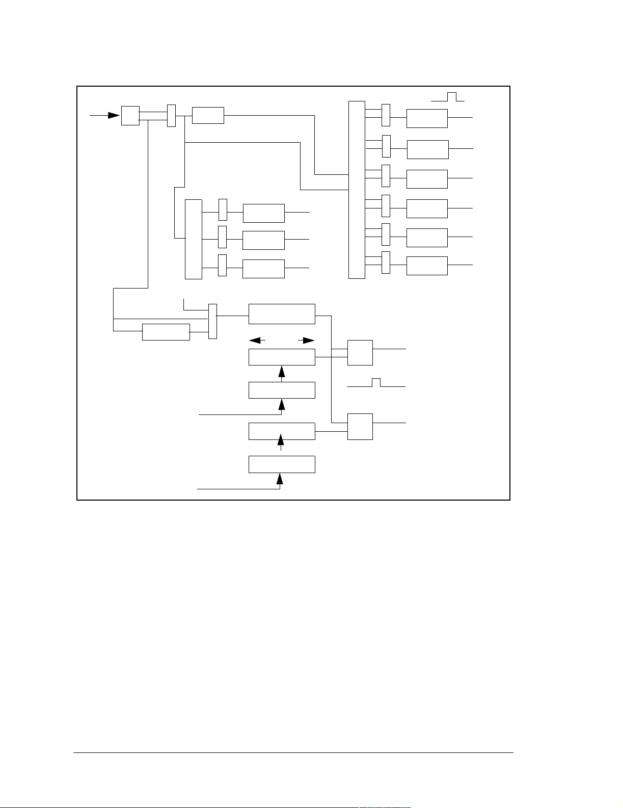
Figure 1-1 shows a block diagram of the Rabbit.
4 Rabbit 3000 Microprocessor
Page 14
/RESET
RESOUT
/IOWR
/IORD
/BUFEN
SMODE0
SMODE1
STATUS
/WDTOUT
CLK
D[7:0]
A[19:0]
XTALA1
XTALA2
CLK32K
ID[7:0]
IA[5:0]
I[7:0]
INT0A, INT1A
INT0B, INT1B
Data
Buffer
Address
Buffer
Spectrum
Spreader
Fast
Oscillator
32.768 kHz
Clock Input
External I/O
Chip Interface
External
Interrupts
Memory
Management/
Control
Clock
Doubler
Global Power
Save & Clock
Distribution
Timer A
Timer B
Real-Time
Clock
Watchdog
Timer
Periodic
Interrupt
External Interface
CPU
(8 bits)
ADDRESS BUS
(8 bits)
DATA BUS
Memory Chip
Interface
Parallel Ports
Port A
Port B
Port C
Port D
Port E
Port F
Port G
Serial Port A
Asynch
Synch
Serial
Serial
Asynch
Synch
Bootstrap
Bootstrap
Asynch Serial IrDA
IrDA Bootstrap
Serial Ports
B,C,D
Asynch
Synch
Serial
Serial
Asynch Serial IrDA
Serial Ports
E, F
Asynch
HDLC
Serial
SDLC
Asynch Serial IrDA
HDLC/SDLC IrDA
Pulse Width
Modulation
Quadrature
Decoder
Input
Capture
Slave Port
Slave Interface
Bootstrap Interface
/CS2, /CS1, /CS0
/OE1, /OE0
/WE1, /WE0
PA [7:0]
PB[7:0]
PC[7:0]
PD[7:0]
PE[7:0]
PF[7:0]
PG[7:0]
TXA, RXA, CLKA,
ATXA, ARXA
TXB, RXB, CLKB,
ATXB, ARXB
TXC, RXC, CLKC
TXD, RXD, CLKD
TXE, RXE
TCLKE, RCLKE
TXF, RXF
TCLKF, RCLKF
PWM[3:0]
QD1A, QD1B
QD2A, QD2B
AQD1A, AQD1B
AQD2A, AQD2B
PC[7,5,3,1]
PD[7,5,3,1]
PF[7,5,3,1]
PG[7,5,3,1]
SD[7:0]
SA[1:0],
/SCS, /SRD, /SWR,
/SLAVEATTN
Figure 1-1. Rabbit 3000 Block Diagram
User’s Manual 5
Page 15

1.2 Summary of Rabbit 3000 Advantages
• The glueless architecture makes it is easy to design the hardware system.
• There are a lot of serial ports and they can communicate very fast.
• Precision pulse and edge generation is a standard feature.
• EMI is at extremely low levels.
• Interrupts can have multiple priorities.
• Processor speed and power consumption are under program control.
• The ultra low power mode can perform computations and execute logical tests since the
processor continues to execute, albeit at 32 kHz or even as slow as 2 kHz.
• The Rabbit may be used to create an intelligent peripheral or a slave processor. For
example, protocol stacks can be off loaded to a Rabbit slave. The master can be any
processor.
• The Rabbit can be cold-booted so unprogrammed flash memory can be soldered in
place.
• You can write serious software, be it 1,000 or 50,000 lines of C code. The tools are
there and they are low in cost.
• If you know the Z80 or Z180, you know most of the Rabbit.
• A simple 10-pin programming interface replaces in-circuit emulators and PROM pro-
grammers.
• The battery-backable time/date clock is included.
• The standard Rabbit chip is made to industrial temperature and voltage specifications.
• The Rabbit 3000 is backed by extensive software development tools and libraries, espe-
cially in the area of networking and embedded Internet.
6 Rabbit 3000 Microprocessor
Page 16

1.3 Differences Rabbit 3000 vs. Rabbit 2000
For the benefit of readers who are familiar with the Rabbit 2000 microprocessor the Rabbit 3000 is contrasted with the Rabbit 2000 in the table below.
Feature Rabbit 3000 Rabbit 2000
Maximum clock speed 54 MHz 30 MHz
Maximum crystal frequency main oscillator (may be
doubled internally)
32.768 kHz crystal oscillator External Internal
Maximum operating voltage 3.6 V 5.5 V
Maximum I/O input voltage 5.5 V 5.5 V
Current consumption 2 mA/MHz @ 3.3 V 4 mA/MHz @5 V
Number of package pins 128 100
16 × 16 × 1.5 mm LQFP
Size of package
Spacing between package pins
Separate power and ground for I/O buffers (EMI
reduction)
Clock Spectrum Spreader (EMI reduction) Yes
Clock Modes 1x, 2x, /2, /3, /4, /6, /8 1x, 2x, /4, /8
0.4 mm (16 mils) LQFP
30 MHz 32 MHz
10 × 10 × 1.2 mm
TFBGA
0.8 mm TFBG A
Yes No
24 × 18 × 3 mm PQFP
0.65 mm (26 mils) PQFP
Rabbit 2000B and
Rabbit 2000C versions.
Sleepy (32 kHz)
Power Down Modes
Low Power Memory Control (Chip Select)
Extended memory timing for high freq. operation Yes No
Number of 8-bit I/O ports 7 5
Auxiliary I/O Data/Address bus Yes None
Number of serial ports 6 4
Serial ports capable of SPI/clocked serial 4 (A, B, C, D) 2 (A, B)
Serial ports capable of SDLC/HDLC 2 (E, F) None
Asynch serial ports with support for IrDA
communications
User’s Manual 7
Ultra-Sleepy
(16, 8, 2 kHz)
Short CS (CLK /4 /6 /8)
Self Timed
(32,16,8,2 kHz)
6None
Sleepy (32 kHz)
None
Page 17

Feature Rabbit 3000 Rabbit 2000
Serial ports with support for SDLC/HDLC IrDA
communications
2None
Maximum asynchronous baud rate clock speed/8 clock speed/32
Input capture unit 2 None
8 Rabbit 3000 Microprocessor
Page 18

2. RABBIT 3000 DESIGN FEATURES
The Rabbit 3000 is an evolutionary design. The processor and instruction set are nearly
identical to the immediate predecessor processor, the Rabbit 2000. Both the Rabbit 3000
and the Rabbit 2000 follow in broad outline the instruction set and the register layout of
the Z80 and Z180. Compared to the Z180 the instruction set has been augmented by a substantial number of new instructions. Some obsolete or redundant Z180 instructions have
been dropped to make available efficient 1-byte opcodes for important new instructions.
(see Chapter 20, “Differences Rabbit vs. Z80/Z180 Instructions,”.) The advantage of this
evolutionary approach is that users familiar with the Z80 or Z180 can immediately understand Rabbit assembly language. Existing Z80 or Z180 source code can be assembled or
compiled for the Rabbit with minimal changes.
Changing technology has made some features of the Z80/Z180 family obsolete, and these
features have been dropped in the Rabbit. For example, the Rabbit has no special support
for dynamic RAM but it has extensive support for static memory. This is because the price
of static memory has decreased to the point that it has become the preferred choice for
medium-scale embedded systems. The Rabbit has no support for DMA (direct memory
access) because most of the uses for which DMA is traditionally used do not apply to
embedded systems, or they can be accomplished better in other ways, such as fast interrupt routines, external state machines or slave processors.
Our experience in writing C compilers has revealed the shortcomings of the Z80 instruction set for executing the C language. The main problem is the lack of instructions for handling 16-bit words and for accessing data at a computed address, especially when the stack
contains that data. New instructions correct these problems.
Another problem with many 8-bit processors is their slow execution and a lack of numbercrunching ability. Good floating-point arithmetic is an important productivity feature in
smaller systems. It is easy to solve many programming problems if an adequate floatingpoint capability is available. The Rabbit’s improved instruction set provides fast floatingpoint and fast integer math capabilities.
The Rabbit supports four levels of interrupt priorities. This is an important feature that
allows the effective use of fast interrupt routines for real-time tasks.
User’s Manual 9
Page 19

2.1 The Rabbit 8-bit Processor vs. Other Processors
The Rabbit 3000 processor has been designed with the objective of creating practical systems to solve real world problems in an economical fashion. A cursory comparison of the
Rabbit 3000 compared to other processors with similar capabilities may miss certain Rabbit strong points.
• The Rabbit is a processor that can be used to build a system in which EMI is nearly
absent, even at clock frequencies in excess of 40 MHz. This is due to the split power
supply, the clock doubler, the clock spectrum spreader and the PC board layout advice
(or processor core modules) that we provide. Low EMI is a huge timesaver for the
designer pressed to meet schedules and pass government EMI tests of the final product.
• Execution speed with the Rabbit is usually a pleasant surprise compared to other processors. This is due to the well-chosen and compact instruction set partnered with and
excellent compiler and library. We have many benchmarks, comparing the Rabbit to
186, 386, 8051, Z180 and ez80 families of processors that prove the point.
• The Rabbit memory bus is an exceptionally efficient and very clean design. No external
logic is required to support static memory chips. Battery-backed external memory is
supported by built-in functionality. During reduced-power slow-clock operation the
memory duty cycle can be correspondingly reduced using built-in hardware, resulting
in low power consumption by the memories.
The Rabbit external bus uses 2 clocks for read cycles and 3 clocks for write cycles. This
has many advantages compared to a single-clock design, and on closer examination the
advantages of the single-clock system turn out to be most ly chimerical. The advantages
include: easy design to avoid bus fights, clean write cycles with solid data and address
hold times, flexibility to have mem ory output ena ble a cce ss t imes gr eate r tha n ½ of the
bus cycle, and the ability to use an asymmetric clock generated by a clock doubler. The
supposed advantage that single-clock systems have of double-speed bus operation is
not possible with real-world memories unless the memory is backed with fast-cache
RAM.
• The Rabbit 3000 operates at 3.6 V or less, but it has 5 V tolerant inputs and has a second complete bus for I/O operations that is separate from the memory bus. This second
auxiliary bus can be enabled by the application as a designer option. These features
make it easy to design systems that mix 3 V and 5 V components, and avoid the loadi ng
problems and the EMI problems that result if the memory bus is extended to connect
with many I/O devices.
• The Rabbit may be remotely programmed, including complete cold-boot, via a serial
link, Ethernet, or even via a network or the Internet using built in capabilities and/or the
RabbitLink ethernet network accessory device. These capabilities proven and inexpensive to implement.
• The Rabbit 3000 on-chip peripheral complement is huge compared to competitive processors.
10 Rabbit 3000 Microprocessor
Page 20

The Rabbit is an 8-bit processor with an 8-bit external data bus and an 8-bit internal data
bus. Because the Rabbit makes the most of its external 8-bit bus and because it has a compact instruction set, its performance is as good as many 16-bit processors.
We hesitate to compare the Rabbit to 32-bit processors, but there are undoubtedly occasions where the user can use a Rabbit instead of a 32-bit processor and save a vast amount
of money. Many Rabbit instructions are 1 byte long. In contrast, the minimum instruction
length on most 32-bit RISC processors is 32 bits.
2.2 Overview of On-Chip Peripherals and Features
The on-chip peripherals were chosen based on our experience as to what types of peripheral devices are most useful in small embedded systems. The major on-chip peripherals
are the serial ports, system clock, time/date oscillator, parallel I/O, slave port, motion
encoders, pulse width modulators, pulse measurement, and timers. These and other features are described below.
2.2.1 5 V Tolerant Inputs
The Rabbit 3000 operates on a voltage in the range of 1.8 V to 3.6 V, but most Rabbit 3000
input pins are 5 V tolerant. The exceptions are the power supply pins, and the oscillator
buffer pins. When a 5 V signal is applied to 5 V tolerant pins, they present a high impedance
even if the Rabbit power is off. The 5 V tolerant feature allows 5 V devices that have a
suitable switching threshold to be directly connected to the Rabbit. This includes HCT
family parts operated at 5 V that have an input threshold between 0.8 and 2 V.
NOTE: CMOS devices operated at 5 V that ha ve a t hreshold at 2.5 V are not suitabl e f or
direct connection because the Rabbit outputs do not rise above VDD, which cannot
exceed 3.6 V, and is often specified as 3.3 V. Although a CMOS input with a 2.5 V
threshold may switch at 3.3 V, it will consume excessive current and switch slowly.
In order to translate between 5 V and 3.3 V, HCT family parts powered from 5 V can be
used, and are often the best solution. There is also the “LVT” family of parts that operate
from 2.0 V to 3.3 V, but that have 5 V tolerant inputs and are available from many suppliers. True level-translating parts are available with separate 3.3 V and 5 V supply pins, but
these parts are not usually needed, and have design traps involving power sequencing.
Many charge pump chips that perform DC to DC voltage conversion at low cost have been
introduced in recent years. These are convenient for systems with dual voltage requirements.
2.2.2 Serial Ports
There are six serial ports designated ports A, B, C, D, E, and F. All six serial ports can
operate in an asynchronous mode up to a baud rate equal to the system clock divided by 8.
The asynchronous ports use 7-bit or 8-bit data formats, with or without parity. A 9th bit
address scheme, where an additional bit is set or cleared to mark the first byte of a message, is also supported.
The serial port software driver can tell when the last byte of a message has finished transmitting from the output shift register - correcting an important defect of the Z180. This is
User’s Manual 11
Page 21

important for RS-485 communication because a half duplex line driver cannot have the
direction of transmission reversed until the last data bit has been sent. In many UARTs,
including those on the Z180, it is difficult to generate an interrupt after the last bit is sent.
A so called address bit can be transmitted as either high or low after the last data bit. The
address bit, if used, is followed by a high stop bit. This facility can be used to transmit 2
stop bits or a parity bit if desired. The ability to directly transmit a high voltage level
address bit was not included in the original revision of the Rabbit 2000 processor.
Serial ports A, B, C and D can be operated in the clocked serial mode. In this mode, a
clock line synchronously clocks the data in or out. Either the Rabbit serial port or the
remote device can supply the clock. When the Rabbit provides the clock, the baud rate can
be up to 1/2 of the system clock frequency. When the clock is provided by another device
the maximum data rate is system clock divided by 6 due to the need to synchronize the
externally supplied clock with the internal clock. The clocked serial mode may be used to
support “SPI” bus devices.
Serial Port A has special features. It can be used to cold-boot the system after reset. Serial
Port A is the normal port that is used for software development under Dynamic C.
All the serial ports have a special timing mode that supports infrared data communications
standards.
2.2.3 System Clock
The main oscillator uses an external crystal with a frequency typically in the range from
1.8 MHz to 26 MHz. The processor clock is derived from the oscillator output by either
doubling the frequency, using the frequency directly, or dividing the frequency by 2, 4, 6
or by 8. The processor clock can also be driven by the 32.768 kHz real-time clock oscillator for very low power operation, in which case the main oscillator can be shut down
under software control.
2.2.4 32.768 kHz Oscillator Input
The 32.768 kHz oscillator input is designed to accept a 32.768 kHz clock. A suggested lowpower clock circuit using “tiny logic” parts is documented and low in cost. The 32.768 kHz
clock is used to drive a battery-backable (there is a separate power pin) internal 48-bit
counter that serves as a real-time clock (RTC). The counter can be set and read by software
and is intended for keeping the date and time. There are enough bits to keep the date for
more than 100 years. The 32.768 kHz oscillator input is also used to drive the watchdog
timer and to generate the baud clock for Serial Port A during the cold-boot sequence.
12 Rabbit 3000 Microprocessor
Page 22
2.2.5 Parallel I/O
There are 56 parallel input/output lines divided among seven 8-bit ports designated A
through G. Most of the port lines have alternate functions, such as serial data or chip select
strobes. Parallel Ports D, E, F, and G have the capability of timer-synchronized outputs.
The output registers are cascaded as shown in Figure 2-1.
Load Data
Load Clock
Tim er Clock
Figure 2-1. Cascaded Output Registers for Pa rallel Ports D and E
Output Port
Stores to the port are loaded in the first-leve l regist er. That register in turn is transferred to
the output register on a selected timer clock. The clock can be selected to be the output of
Timer A1, B1, B2 or the peripheral clock (divided by 2?). The timer signal can also cause
an interrupt that can be used to set up the ne xt bit to be output on the next timer pulse . This
feature can be used to generate precisely controlled pulses whose edges are positioned
with high accuracy in time. Applications include communications signaling, pulse width
modulation and driving stepper motors. (A separate pulse width modulation facility is also
included in the Rabbit 3000.)
External Input
D Q D Q
Filtered Input
peripheral
clock
Figure 2-2. Digital Filtering Input Pins
Input pins to the parallel ports are filtered by cascaded D flip flops as shown in Figure 2-2.
This prevents pulses shorter then the peripheral clock from being recognized, synchronizes external pulses to the internal clock, and avoids problems with meta stability (temporarily indeterminate logical conditions due to marginal set up time with respect to the
clock).
User’s Manual 13
Page 23
2.2.6 Slave Port
The slave port is designed to allow the Rabbit to be a slave to another processor, which
could be another Rabbit. The port is shared with Parallel Port A and is a bidirectional data
port. The master can read any of three registers selected via two select lines that form the
register address and a read strobe that causes the register contents to be output by the port.
These same registers can be written as I/O registers by the Rabbit slave. Three additional
registers transmit data in the opposite direction. They are written by the master by means
of the two select lines and a write strobe.
Figure 2-3 shows the data paths in the slave port.
Rabbit 3000
Master
Processor
Input Register
CPU
Output Registers
Control
Figure 2-3. Slave-Port Data Paths
Slave Interface Registers
The slave Rabbit can read the same registers as I/O registers. When incoming data bits are
written into one of the registers, status bits indi cate whi ch registers have bee n written, and
an optional interrupt can be programmed to take place when the write occurs. When the
slave writes to one of the registers carrying data bits outward, an attention line is enabled
so that the master can detect the data change and be interrupted if desired. One line tells
the master that the slave has read all the incoming data. Another line tells the master that
new outgoing data bits are available and have not yet been read by the master. The slave
port can be used to signal the master to perform tasks using a variety of communication
protocols over the slave port.
14 Rabbit 3000 Microprocessor
Page 24

2.2.7 Auxiliary I/O Bus
The Rabbit 3000 instruction set supports memory access and I/O access. Memory access
takes place in a 1 megabyte memory space. I/O access takes place in a 64K I/O space. In a
traditional microprocessor design the same address and data lines are used for both memory and I/O spaces. Sharing address and data lines in this manner of ten force s compr omises
or makes design more complic ated. Gene rally the me mory bus ha s more crit ical timing a nd
less tolerant of additional capacitive loading imposed by sharing it with an I/O bus.
With the Rabbit 3000, the designer has the option of enabling completely separate buses
for I/O and memory. The auxiliary I/O bus uses many of the same pins used by the slave
port, so its operation is mutually exclusive fr om operation of the slave port. Parallel Port A
is used to provide 8 bidirectional data lines. Parallel Port B bits 2:7 provide 6 address
lines, the least significant 6 lines of the 16 lines that define the full I/O space. The auxiliary bus is only active on I/O bus cycles. The address lines remain in the same state
assumed at the end of the previous I/O cycle until another I/O cycle takes place. I/O chip
selects as well as read and write strobes are available at various other pins so that the 64
byte space defined by the 6 address lines may be easily expanded. I/O cycles also execute
in parallel on the main (memory) bus when they take place on the auxiliary bus, so additional address lines can be buffered and provided if needed.
By connecting I/O devices to the auxiliary bus, the fast memory bus is relieved of the
capacitive load that would otherwise slow the memory. For core modules based on the
Rabbit 3000, fewer pins are required to exit the core module since the slave port and the
I/O bus can share the same pins and the memory bus no longer needs to exit the module to
provide I/O capability. Because the I/O bus has less activity and is slower than the memory
bus, it can be run further physi cally without EMI and ground boun ce problems. 5 V signals
can appear on the I/O bus since the Rabbit 3000 inputs are 5 V tolerant. 5 V signals could
easily cause problems on the main bus if non 5 V tolerant 3.3 V memories are connected.
2.2.8 Timers
The Rabbit has several timer systems. The periodic interrup t is driven by the 32. 768 kHz
oscillator divided by 16, g iving an i nterrupt every 4 88 µs if enabled. This is int ended to be
used as a general-purpose clock interrupt. Timer A consists of ten 8-bit countdown and
reload registers that can be cascaded up to two levels deep. Each countdown register can be
set to divide by any number between 1 and 256. The output of six of the timers is used to
provide baud clocks for the serial ports. Any of these registers can also cause interrupts and
clock the timer-sy nchronized parallel outpu t ports. T imer B consists of a 10-bit counter that
can be read but not written. There are two 10-bit match registers and comparators. If the
match register matches the coun ter , a pulse is outpu t. Thus th e timer c an be pro gramm ed to
output a pulse at a predetermined count in the future. This pulse can be used to clock the
timer-synchronized parallel-port output registers as well as cause an interrupt. Timer B is
convenient for creating an event at a precise time in the future under program control.
Figure 2-4 illustrates the Rabbit timers.
User’s Manual 15
Page 25
perclk
perclk
perclk/2
A1
Timer A System
Serial E
A2
Serial F
A3
Timer A1
perclk/2
perclk/8
Timer B System
A8
A9
A10
10-bit counter
match preload
match preload
Input
Capture
PWM
Quadrature
Decode
10 bits
match reg
match reg
A4
Serial A
Serial B
A5
Serial C
A6
Serial D
A7
compare
Timer_B1
Control Timer
Synchronized
outputs
Timer_B2
Figure 2-4. Rabbit Timers A and B
2.2.9 Input Capture Channels
The input capture channels are used to determine the time at which an event takes place.
An event is signaled by a rising or falling edge (or optionally by either edge) on one of 16
input pins that can be selected as input for either of the two channels. A 16 bit counter is
used to record the time at which the event takes place. The counter is driven by the output
of Timer A8 and can be set to count at a rate ranging from full clock speed to 1/256 the
clock speed.
T wo events are recognized: a start condi tion and a stop condition. The start c ondition may
be used to start counting and the stop condition to stop counting. However the counter
may also run continuously or run until a stop condition is encountered. The start and stop
conditions may also be used to latch the current time at the instant the condition occurs
rather than actually start or stop the counter. The same pin may be used to detect the start
16 Rabbit 3000 Microprocessor
Page 26

and stop condition, for example a rising edge could be the start condition and a falling
edge the stop condition. However, optionally, the start and stop condition can be input
from separate pins.
The input capture channels can be used to measure the width of fast pulses. This is done
by starting the counter on the first edge of the pulse and capturing the counter value on the
second edge of the pulse. In this case the maximum error in the measurement is approximately 2 periods of the clock used to count the counter. If there is sufficient time between
events for an interrupt to take place the unit can be set up to capture the counter value on
either start or stop conditions or both and cause an interrupt each time the count is captured. In this case the start and stop conditions lose the connection with starting or stopping the counter and simply become capture conditions that may be specified for 2
independent edge detectors. The counter can also be cleared and started under software
control and then have its value captured in response to an input.
If desired the capture counter can synchronized with Timer B outputs used to synchronously load parallel port output registers. This makes it possible to generate an output signal precisely synchronized with an input signal. Usually it will be desired to synchronize
one of the input capture counters with the Timer B counter. The count offset can be measured by outputting a pulse at a precise time using Timer B to set the output time and capturing the same pulse. Once the phase relationship is known between the counters it is then
possible to output pulses a precise time delay after an input pulse is captured, provided
that the time delay is great enough for the interrupt routine to processes the capture event
and set up the output pulse synchronized by Timer B. The minimum time delay needed is
probably less than 10 microseconds if the software is done carefully the clock speed is reasonably high.
2.2.10 Quadrature Encoder Inputs
A quadrature encoder is a common electromechanical device used to track the rotation of
a shaft, or in some cases to track the motion of a linear fo llower. These devices are usually
implemented by the use of a disk or a strip with alternate opaque and transparent bands
that excite dual optical detectors. The output signals are square waves 90 degrees out of
phase also called being in quadrature with each other. By having quadrature signals, the
direction of rotation can be detected by noting which signal leads the other signal.
The Rabbit 3000 has 2 quad rat ur e enco der uni ts . Ea ch un it has 2 inpu t s, one be in g the no rmal input and the other the 90 degree or quadrature input. An 8 bit up down counter counts
encoder steps in the forward and backw ard dire ction. The cou nt can be exte nd ed beyon d 8
bits by an interrupt that takes pl ace each time the count overf lows or und erflows. The external signals are synchronized with an internal clock provided by the output of Timer A10.
2.2.11 Pulse Width Modulation Outputs
The pulse width modulated output generates a train of pulses periodic on a 1024 pulse
frame with a duty cycle that varies from 1/1024 to 1024/1024. There are 4 independent
PWM units. The units are driv en by the out put of Timer A9 which may be used to vary the
User’s Manual 17
Page 27

length of the pulses. When the duty cycle is greater then 1/1024 the pulses are spread into
groups distributed 2 56 counts apart in th e 1024 frame. The puls e width modu lation output s
can be passed through a filter and used as a 10-bit D/A converter. The outputs can also be
used to directly drive devices that have intrinsic filtering such as motors or solenoids.
2.2.12 Spread Spectrum Clock
The main system clock, which is generated by the crystal oscillator or input from an external oscillator, can be modified by a clock spectrum spreader internal to the Rabbit 3000
chip. When the spectrum spreader is engaged, the clock is alternately speeded up and
slowed down, thus spreading the spectrum of the clock harmonics in the frequency
domain. This reduces EMI and improves the results of official radiated-emissions tests
typically by 15–20 dB at critical frequencies. The spectrum spreader has 3 modes of operation: off, normal, and strong. Slightly faster memory access time is required when the
spectrum spreader is used: 2–3 ns for the normal setting when the clock doubler is
enabled, and 6–9 ns for the strong setting when the clock doubler is used. The spreader
slightly influences baud rates and other timings because it introduces clock jitter, but the
effect is usually small enough to be negligible.
2.2.13 Separate Cor e and I/O Power Pins
The silicon die that constitutes the Rabbit 3000 processor is divided in to the core logic and
the I/O ring. The I/O ring located on the 4 edges of the die holds the bonding pads and the
large transistors use d to cre ate the I/ O buffers that drive signals to the external world. The
core section, inside the I/O ring contains the main processor and peripheral logic. The
clock and clock edges in the core are very fast with large transient currents that create a lot
of noise that is communicated to the outside of the package via the power pins. The I/O
buffers have slower switching times and mostly operate at much lower frequencies than
the core logic. The Rabbit has separate power and ground pins for the core and I/O ring.
This allows the designer to feed clean power to the I/O ring filtered to be free of the noise
generated by the core switching. This minimizes high frequency noise that would otherwise appear on output pins driven by buffers in the I/O ring. The result is lower EMI.
2.3 Design Standards
The same functionality can often be accomplished in more than one way with the Rabbit
3000. By publishing design standards, or standard ways to accomplish common objec-
tives, software and hardware support become easier.
Refer to the Rabbit 3000 Microprocessor Designer’ s Handbook for additional information.
2.3.1 Programming Port
Rabbit Semiconductor publishes a specification for a standard programming port (see
Appendix A, “The Rabbit Programming Port”) and provides a converter cable that may be
used to connect a PC serial port to the standard programming interface. The interface is
implemented using a 10-pin connector with two rows of pins on 2 mm centers. The port is
connected to Rabbit Serial Port A, to the startup mode pins on the Rabbit, to the Rabbit
18 Rabbit 3000 Microprocessor
Page 28

reset pin, and to a programmable output pin that is used to signal the PC that attention is
needed. With proper precautions in design and software, it is possible to use Serial Port A
as both a programming port and as a user-defined serial port, although this will not be necessary in most cases.
Rabbit Semiconductor supports the use of the standard programming port and the standard
programming cable as a diagnostic and setup port to diagnosis problems or set up systems
in the field.
2.3.2 Standard BIOS
Rabbit Semiconductor provides a standard BIOS for the Rabbit. The BIOS is a software
program that manages startup and shutdown, and provides basic services for software running on the Rabbit.
2.4 Dynamic C Support for the Rabbit
Dynamic C is Z-World’s interactive C language development system. Dynamic C runs on
a PC under Windows 32-bit operating systems. Dynamic C provides a combined compiler,
editor, and debugger. The usual method for debugging a target system based on the Rabbit
is to implement the 10-pin programming connector that connects to the PC serial port via a
standard converter cable. Dynamic C libraries contain highly perfected software to control
the Rabbit. These includes drivers, utility and math routines and the debugging BIOS for
Dynamic C.
In addition, the internationally known real-time operating system, uC/OS-II, has been
ported to the Rabbit, and is available with Dynamic C on a license-free, royalty-free basis
for use in Rabbit-based products..
User’s Manual 19
Page 29

20 Rabbit 3000 Microprocessor
Page 30
3. DETAILS ON RABBIT
MICROPROCESSOR FEATURES
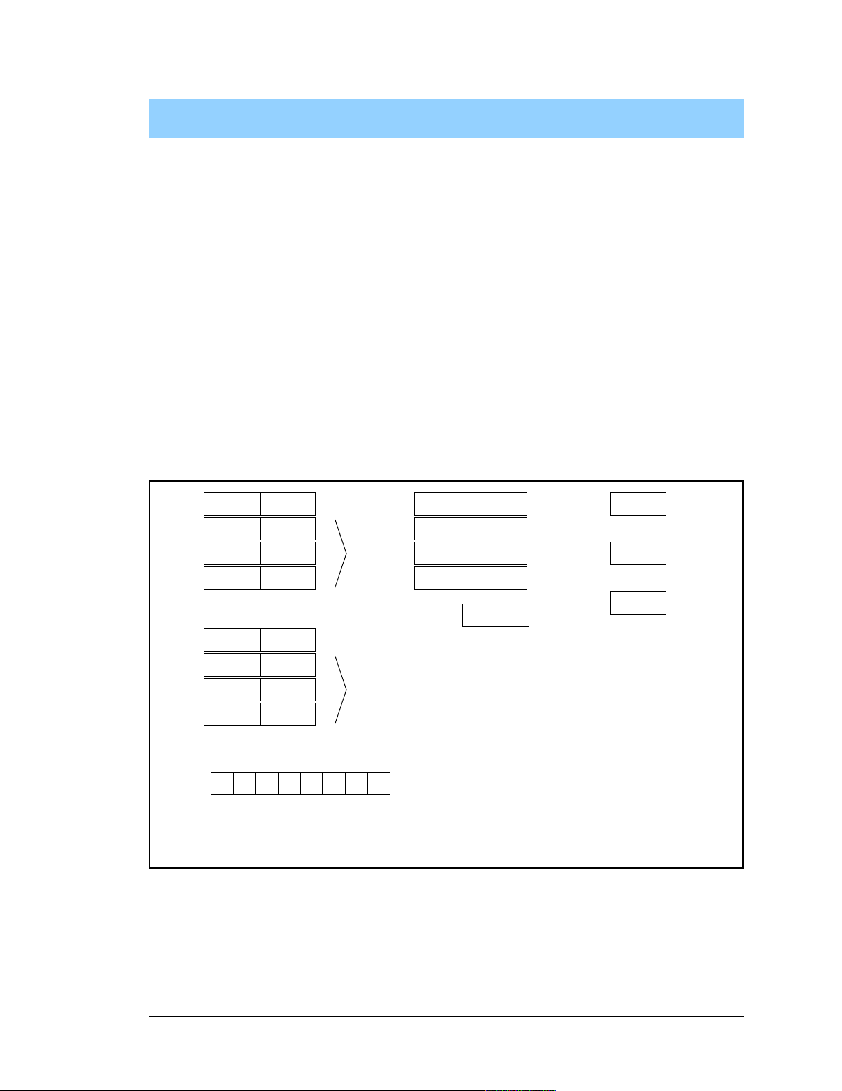
3.1 Processor Registers
The Rabbit’s registers are nearly identical to those of the Z180 or the Z80. The figure
below shows the register layout. The XPC and IP registers are new. The EIR register is the
same as the Z80 I register, and is used to point to a table of interrupt vectors for the externally generated interrupts. The IIR register occupies the same logical position in the
instruction set as the Z80 R register, but its function is to point to an interrupt vector table
for internally generated interrupts.
A
H
D
B
A'
H '
D '
B '
F
L
E
C
L'
E '
C '
8/16-bit
registers
F '
Alternate Registers
SZ V C
S-sign, Z-zero, V-overflow, C-carry
Bits marked "x" are read/write.
xxx x
F - flag register layout
Figure 3-1. Rabbit Registers
IX
IY
SP
PC
XPC
IP
IIR
EIR
A- 8-bit accumulator
F - flags register
HL- 16-bit accumulator
IX, IY - Index registers/alt accum’s
SP - stack pointer
PC- program counter
XPC - extension of program counter
IIR - internal interrupt register
EIR-external interrupt register
IP - interrupt priority register
User’s Manual 21
Page 31

The Rabbit (and the Z80/Z180) processor has two accumulators—the A register serves as
an 8-bit accumulator for 8-bit operations such as ADD or AND. The 16-bit register HL regis-
ter serves as an accumulator for 16-bit operations such as ADD HL,DE, which adds the 16bit register DE to the 16-bit accumulator HL. For many operations IX or IY can substi tute
HL as accumulators.
for
The register marked F is the flags register or status register. It holds a number of flags that
provide information about the last operation performed. The flag register cannot be
accessed directly except by using the POP AF and PUSH AF instructions. Normally the
flags are tested by conditional jump instructions. The flags are set to mark the results of
arithmetic and logic operations according to rules that are specified for each instruction.
There are four unused read/write bits in the flag register that are available to the user via
the PUSH AF and POP AF instructions. These bits should be used with caution since newgeneration Rabbit processors could use these bits for new purposes.
The registers IX, IY and HL can also serve as index registers. They point to memory
addresses from which data bits are fetched or stored. Although the Rabbit can address a
megabyte or more of memory, the index registers can only directly address 64K of memory (except for certain extended addressing LDP instructions). The addressing range is
expanded by means of the memory mapping hardware (see “Memory Mapping” on
page 23) and by special instructions. For most embedded applications, 64K of data memory (as opposed to code memory) is sufficient. The Rabbit can efficiently handle a megabyte of program space.
The register SP points to the stack that is used for subroutine and interrupt linkage as well
as general-purpose storage.
A feature of the Rabbit (and the Z80/Z180) is the alternate register set. Two special
instructions swap the alternate regist ers with the regular registers. The instruction EX AF,AF’
exchanges the contents of AF with AF'. The instruction EXX exchanges HL, DE, and BC
with HL', DE', and BC'. Communication between the regular and alternate register set in
the original Z80 architecture was difficult because the exchange instructions provided the
only means of communication between the regular and alternate register sets. The Rabbit
has new instructions that greatly improve communication between the regular and alternate register set. This effectively doubles the number of registers that are easily available
for the programmer’s use. It is not intended that the alternate register set be used to provide a separate set of registers for an interrupt routine, and Dynamic C does not support
this usage because it uses both registers sets freely.
The IP register is the interrupt priority register. It contains four 2-bit fields that hold a history of the processor’s interrupt priority. The Rabbit supports four levels of processor priority, something that exists only in a very restricted form in the Z80 or Z180.
22 Rabbit 3000 Microprocessor
Page 32

3.2 Memory Mapping
Although the Rabbit memory mapping scheme is fairly complex, the user rarely needs to
worry about it because the details are handled by the Dynamic C development system.
Except for a handful of special instructions (see Section 19.5, “16-bit Load and Store 20bit Address”.), the Rabbit instructions directly address a 64K data memory space. This
means that the address fields in the instructions are 16 bits long and that the registers that
may be used as pointers to memory addresses (index registers (IX, IY), program counter
and stack pointer (SP)) are also 16 bits long.
Because Rabbit instructions use 16-bit addresses, the instructions are shorter and can execute much faster than if, for example, 32-bit addresses were used. The executable code is
very compact.
The Rabbit memory-mapping unit is similar to, but more powerful than, the Z180 memory-mapping unit. Figure 3-2 illustrates the relationship among the major components
related to addressing memory.
Processor
Memory
Mapping
16
Unit
bits
Figure 3-2. Addressing Memory Components
20
bits
Memory
Interface
Memory
Chips
20 bits plus control
The memory-mapping unit receives 16-bit addresses as input and outputs 20-bit addresses.
The processor (except for certain LDP instructions) sees only a 16-bit address space. That
is, it sees 65536 distinctly addressable bytes that its instructions can manipulate. Three
segment registers are used to map this 16-bit space into a 1-megabyte space. The 16-bit
space is divided into four separate zones. Each zone, except the first or root zone, has a
segment register that is added to the 16-bit address within the zone to create a 20-bit
address. The segment register has eight bits and those eight bits are added to the upper
four bits of the 16-bit address, creating a 20-bit address. Thus, each separate zone in the
16-bit memory becomes a window to a segment of memory in the 20-bit address space.
The relative size of the four segments in the 16-bit space is controlled by the SEGSIZE
register. This is an 8-bit register that contains two 4-bit registers. This controls the boundary between the first and the second segment and the boundary between the second and
the third segment. The location of the two movable segment boundaries is determined by a
4-bit value that specifies the upper four bits of the address where the boundary is located.
These relationships are illustrated in Figure 3-3.
User’s Manual 23
Page 33

10000
SEGSIZE
register
85
80
79
XPC register
STACKSEG register
DATASEG register
10000
XPC
segment
E000
stack segment
D000
data segment
7D
7000
0E000
85
93000
0D000
80
8D000
07000
79
80000
root segment
0000
16-bit
address space
20-bit
address space
Figure 3-3. Example of Memory Mapping Operation
07000
00000
The names given to the segments in the figure are evocative of the common uses for each
segment. The root segment is mapped to the base of flash memory and contains the startup
code as well as other code that may happen to be stored there. The data segment usage
varies depending on the overall strategy for setting up memory. It may be an extension of
24 Rabbit 3000 Microprocessor
Page 34

the root segment or it may contain data variables. The stack segment is normally 4K long
and it holds the system stack. The XPC segment is normally used to execute code that is
not stored in the root segment or the data segment. Special instructions support executing
code that is visible in the XPC segment.
The memory interface unit receives the 20-bit addresses generated by the memory-mapping unit. The memory interface unit conditionally modifies address lines A16, A18 and
A19. The other address lines of the 20-bit address are passed unconditionally. The memory interface unit provides control signals for external memory chips. These interface signals are chip selects (/CS0, /CS1, /CS2), output enables (/OE0, /OE1), and write enables
WE0, /WE1). These signals correspond to the normal control lines found on static mem-
(/
ory chips (chip select or /CS, output enable or /OE, and write enable or /WE). In order to
generate these memory control signals, the 20-bit address space is divided into four quadrants of 256K each. A bank control register for each quadrant determines which of the
chip selects and which pair of output enables, and write enables (if any) is enabled when a
memory read or write to that quadrant takes place. For example, if a 512K x 8 flash memory is to be accessed in the first 512K of the 20-bit address space, then /CS0, /WE0, /OE0
could be enabled in both quadrants.
Figure 3-4 shows a memory interface unit.
Axxin—from processor
Axx—out from memory
control unit
Address lines not shown
are passed directly.
A19in
Optional A19 inversion
Read/Write
Synchronization
A19in
A18in
A19in'
A18in
memory
control
Figure 3-4. Memory Interface Unit
A19
A18
A18, A19 invertible
by quadrant
/CS0
/CS1
/CS2
/OE0
/WE0
/OE1
/WE1
memory
control
lines
User’s Manual 25
Page 35

3.2.1 Extended Code Space
A crucial element of the Rabbit memory mapping scheme is the ability to execute programs containing up to a megabyte of code in an efficient manner. This ability is absent in
a pure 16-bit address processor, and it is poorly supported by the Z180 through its memory
mapping unit. On paged processors, such as the 8086, this capability is provided by paging
the code space so that the code is stored in many separate pages. On the 8086 the page size
is 64K, so all the code within a given page is accessible using 16-bit addressing for jumps,
calls and returns. When paging is used, a separate register (CS on the 8086) is used to
determine where the active page currently resides in the total memory space. Special
instructions make it possible to jump, call or return from one page to another. These special instructions are called long calls, long jumps and long returns to distinguish them
from the same operations that only operate on 16-bit variables.
The Rabbit also uses a paging scheme to expand the code space beyond the reach of a 16bit address. The Rabbit paging scheme uses the concept of a sliding page, which is 8K
long. This is the XPC segment. The 8-bit XPC register serves as a page register to specify
the part of memory where the window points. When a program is executed in the XPC
segment, normal 16-bit jumps, calls and returns are used for most jumps within the window. Normal 16-bit jumps, calls and returns may also be used to access code in the other
three segments in the 16-bit address space. If a transfer of control to code outside the window is required, then a long jump, long call or long return is used. These instructions modify both the program counter (PC) and the XPC register, causing the XPC window to point
to a different part of memory where the target of the long jump, call or return is located.
The XPC segment is always 8K long. The granularity with which the XPC segment can be
positioned in memory is 4K. Because the window can be slid by one-half of its size, it is
possible to compile continuously without unused gaps in memory.
As the compiler generates code resident in the XPC window, the window is slid down by
4K when the code goes beyond F000. This is accomplished by a long jump that repositions the window 4K lower . This is illustrated by Figure 3-5. The compiler is not presented
with a sharp boundary at the end of the page because the window does not run out of space
when code passes F000 unless 4K more of code is added before the window is slid down.
All code compiled for the XPC window has a 24-bit address consisting of the 8-bit XPC
and the 16-bit address. Short jumps and calls can be used, provided that the source and target instructions both have the same XPC address. Generally this means that each instruction belongs to a window that is approximately 4K long and has a 16-bit address between
E000+n and F000+m, where n and m are on the order of a few dozen bytes, but can be up
to 4096 bytes in length. Since the window is limited to no more than 8K, the compiler is
unable to compile a single expression that requires more than 8K or so of code space. This
is not a practical consideration since expressions longer than a few hundred bytes are in
the nature of stunts rather than practical programs.
Program code can reside in the root segment or the XPC segment. Program code may also
be resident in the data segment. Code can be executed in the stack segment, but this is usually restricted to special situations. Code in the root, meaning any of the segments other
26 Rabbit 3000 Microprocessor
Page 36

than the XPC segment, can call other code in the root using short jumps and calls. Code in
the XPC segment can also call code in the root using short jumps and calls. However, a
long call must be used when code in the XPC segment is called. Functions located in the
root have an efficiency advantage because a long call and a long return require 32 clocks
to execute, but a short call and a short return require only 20 clocks to execute. The difference is small, but significant for short subroutines.
10000
E000
D000
XPC segment
Stack segment
Data segment
Root segment
Compiler notices that
code has passed F000.
short
calls
returns
XPC=N
PC=F000+K
Illustration of sliding XP C window
Figure 3-5. Use of XPC Segment
Compiler inserts
long jump in code.
F000
E000
XPC=N+1
PC=E000+K+4
3.2.2 Separate I and D Space - Ex tending Data Memory
In the normal memory model, the data space must share a 64K space with root code, the
stack, and the XPC window. Typically, this leaves a potential data space of 40K or less.
The XPC requires 8K, the stack requires 4K, and most s ystems will require at least 12K of
root code. This amount of data space is sufficient for many embedded applications.
One approach to getting more data space is to place data in RAM or in flash memory that
is not mapped into the 64K space, and then access this data using function calls or in
assembly language using the LDP instructions that can access memory using a 20-bit
address. This greatly expands the data space, but the instructions are less efficient than
instructions that access the 64k space using 16 bit addresses.
The Rabbit 3000 supports separate I and D or Instruction and Data spaces. When separate
I and D space is enabled it applies only to addresses in the root segment or data segment.
Separate I and D spaces mean that instruction execution makes a distinction between
User’s Manual 27
Page 37

fetching an instruction from memory and fetching or storing data in memory. When
enabled separate I and D space make available the combined root and data segment, typically 52k bytes for root code in the I space. In the D space, the root code segment part of
the D space is typically used for constant data mapped to flash memory while the data segment part of the D space is used for variable data mapped to RAM. Separate I and D space
increases the amount of both root code and root data because they no longer have to share
the same memory, even though they share the same addresses.
20 Bit Memory Space
RAM
64k
xpc
56k
window
512k
D Space
stack
52k
Flash
Variable
128k
D Space
I space
Data
Segment
Root
Code
64k
Root
Segment
Figure 3-6. Separate I and D Space
Constant
D Space
Normally separate I and D space is implemented as shown in Figure 3-6. In the I space the
root segment and the data segment are combined into a single root code segment. In the D
space the segments are separately mapped to flash and RAM to provide storage for constant data and variable data. The hardware method to achieve separate 20 bit addresses for
the D space is to invert either A16 or A19 for data accesses. The inversion may be specified separately for the root segment and the data segment. Normally A16 is inverted for
data accesses in the root segment. This causes data accesses to the root segment to be
moved 64k higher to a section of flash starting at 20 bit address 64k that is reserved for
constant data. A19 is normally inverted for data accesses to the data segment, causing the
data accesses in the data segment to be moved to an address 512k higher in the 20 bit
space, an address normally mapped to RAM. The stack segment and the XPC segment do
28 Rabbit 3000 Microprocessor
Page 38

not have split I and D space and memory accesses to these segments do not distinguish
between I and D space.
The advantage of having more root code space is that root code executes faster because
short calls using a 16 bit address are used to call it. This compares to long calls that have a
20 bit address for extended code. Data located in the root can be more conveniently
accessed due to the comparatively limited instructions available for accessing data in the
full 20 bit space and the greater overhead involve in manipulating 20 bit addresses in a
processor that has 8 and 16 bit registers.
3.2.3 Using the Stack Segment for Data Storage
Another approach to extending data memory is to use the stack segment to access data,
placing the stack in the data segment so as to free up the stack segment. This approach
works well for a software system that uses data groupings that are self-contained and are
accessed one at a time rather than randomly between all the groupings. An example would
be the software structures associated with a TCP/IP communication protocol connection
where the same code accesses the data structures associated with each connection in a pattern determined by the traffic on each connection.
The advantage of this approach is that normal C data access techniques, such as 16-bit
pointers, may be used. The stack segment register has to be modified to bring the data
structure into view in the stack segment before operations are performed on a particular
data structure. Since the stack has to be moved into the data area, it is important that the
number of stacks required be kept to a minimum when using the stack segment to view
data. Of course, tasks that don’t need to see the data st ructures can have their stack located
in the stack segment. Another possibility is to have a data structure and a stack located
together in the stack segment, and to use a different stack segment for different tasks, each
task having its own data area and stack bound to it.
These approaches are shown in Figure 3-7 below.
User’s Manual 29
Page 39

Data
(RAM)
Root
Code
(flash)
Stack Segment
used as data
window
Data Segment
used as data
window
Stacks in data
segment
Root Segment
mapped to
RAM has both
root code and
data.
Stack Segment
used for stack
Data
(RAM)
Root
Code
(RAM)
Using Stack Segment
for a Data Wi ndo w
Figure 3-7. Schemes for Data Memory Windows
Using Data S e gment for
a Data Window (Code must
be copied to RAM on startup.)
A third approach is to place the data and root code in RAM in the root segment, freeing the
data segment to be a window to extended memory. This requires copying the root code to
RAM at startup time. Copying root code to RAM is not necessarily that burdensome since
the amount of RAM required can be quite small, say 12K for example.
The XPC segment at the top of the memory can also be used as a data segment by programs that are compiled into root memory. This is handy for small programs that need to
access a lot of data.
3.2.4 Practical Memory Considerations
The simplest Rabbit configurations have one flash memory chip interfaced using /CS0 and
one RAM memory chip interfaced using /CS1. T ypical Rabbit-based systems use 256K of
flash and 128 K of RAM, but smaller or larger memories may be used.
Although the Rabbit can support code size approaching a megabyte, it is anticipated that
the majority of applications will use less than 250K of code, equivalent to approximately
10,000–20,000 C statements. This reflects both the compact nature of Rabbit code and the
typical size of embedded applications.
Directly accessible C variables are limited to approximately 44K of memory, split
between data stored in flash and RAM. This will be more than adequate for many embed-
30 Rabbit 3000 Microprocessor
Page 40

ded applications. Some applications may require large data arrays or tables that will
require additional data memory. For this purpose Dynamic C supports a type of extended
data memory that allows the use of additional data memory, even extending far beyond a
megabyte.
Requirements for stack memory depend on the type of application and particularly
whether preemptive multitasking is used. If preemptive multitasking is used, then each
task requires its own stack. Since the stack has its own segment in 16-bit address space, it
is easy to use available RAM memory to support a large number of stacks. When a preemptive change of context takes place, the STACKSEG register can be changed to map
the stack segment to the portion of RAM memory that contains the stack associated with
the new task that is to be run. Normally the stack segment is 4K, which is typically large
enough to provide space for several (typically four) stacks. It is possible to enlarge the
stack segment if stacks larger than 4K are needed. If only one stack is needed, then it is
possible to eliminate the stack segment entirely and place the single stack in the data segment. This option is attractive for systems with only 32K of RAM that don’t need multiple
stacks.
User’s Manual 31
Page 41

3.3 Instruction Set Outline
“Load Immediate Data to a Register” on page 33
“Load or Store Data from or to a Constant Address” on page 33
“Load or Store Data Using an Index Register” on page 34
“Register-to-Register Move” on page 35
“Register Exchanges” on page 35
“Push and Pop Instructions” on page 36
“16-bit Arithmetic and Logical Ops” on page 36
“Input/Output Instructions” on page 39—these include a fix for a bug that manifests itself
if an I/O instruction (prefix IOI or IOE) is followed by one of 12 single-byte op codes that
use HL as an index register.
In the discussion that follows, we give a few example instructions in each general category
and contrast the Z80/ Z180 with the Rabbit. For a detailed description of every instruction,
see Chapter 19, “Rabbit Instructions”
The Rabbit executes instructions in fewer clocks then the Z80 or Z180. The Z180 usually
requires a minimum of four clocks for 1-byte opcodes or three clocks for each byte for
multi-byte op codes. In addition, three clocks are required for each data byte read or written. Many instructions in the Z180 require a substantial number of additional clocks. The
Rabbit usually requires two clocks for each byte of the op code and for each data byte
read. Three clocks are needed for each data byte written. One additional clock is required
if a memory address needs to be computed or an index register is used for addressing.
Only a few instructions don’t follow this pattern. An example is mul, a 16 x 16 bit signed
two’s complement multiply. mul is a 1-byte op code, but requires 12 clocks to execute.
Compared to the Z180, not only does the Rabbit require fewer clocks, but in a typical situation it has a higher clock speed and its instructions are more powerful.
The most important instruction set improvements in the Rabbit over the Z180 are in the
following areas.
• Fetching and storing data, especially 16-bit words, relative to the stack pointer or the
index registers IX, IY, and HL.
• 16-bit arithmetic and logical operations, including 16-bit and’s, or’s, shifts and 16-bit
multiply.
• Communication between the regular and alternate registers and between the index registers and the regular registers is greatly facilitated by new instructions. In the Z180 the
alternate register set is difficult to use, while in the Rabbit it is well integrated with the
regular register set.
• Long calls, long returns and long jumps facilitate the use of 1M of code space. This
removes the need in the Z180 to utilize inefficient memory banking schemes for larger
programs that exceed 64K of code.
32 Rabbit 3000 Microprocessor
Page 42

• Input/output instructions are now accomplished by normal memory access instructions
prefixed by an op code byte to indicate access to an I/O space. There are two I/O
spaces, internal peripherals and external I/O devices.
Some Z80 and Z180 instructions have been deleted and are not supported by the Rabbit
(see Chapter 20, “Differences Rabbit vs. Z80/Z180 Instructions”). Most of the deleted
instructions are obsolete or are little-used instructions that can be emulated by several
Rabbit instructions. It was necessary to remove some instructions to free up 1-byte op
codes needed to implement new instructions efficiently. The instructions were not reimplemented as 2-byte op codes so as not to waste on-chip resources on unimportant
instructions. Except for the instruction
EX (SP),HL, the original Z180 binary encoding
of op codes is retained for all Z180 instructions that are retained.
3.3.1 Load Immediate Data to a Register
A constant that follows the op code in the instruction stream can generally be loaded to
any register, except PC, IP, and F. (Load to the PC is a jump instruction.) This includes the
alternate registers on the Rabbit, but not on the Z180. Some example instructions appear
below.
LD A,3
LD HL,456
LD BC',3567 ; not possible on Z180
LD H',0x4A ; not possible on Z180
LD IX,1234
LD C,54
Byte loads require four clocks, word loads require six clocks. Loads to IX, IY or the alternate registers generally require two extra clocks because the op code has a 1-byte prefix.
3.3.2 Load or Store Data from or to a Constant Address
LD A,(mn) ; loads 8 bits from address mn
LD A',(mn) ; not possible on Z180
LD (mn),A
LD HL,(mn) ; load 16 bits from the address specified by mn
LD HL',(mn) ; to alternate register, not possible Z180
LD (mn),HL
Similar 16-bit loads and stores exist for DE, BC, SP, IX and IY.
It is possible to load data to the alternate registers, but it is not possible to store the data in
the alternate register directly to memory.
LD A’,(mn) ; allowed
** LD (mn),D’ ; **** not a legal instruction!
** LD (mn),DE’ ; **** not a legal instruction!
User’s Manual 33
Page 43

3.3.3 Load or Store Data Using an Index Register
An index register is a 16-bit register, usually IX, IY, SP or HL, that is used for the address
of a byte or word to be fetched from or stored to memory. Sometimes an 8-bit offset is
added to the address either as a signed or unsigned number. The 8-bit offset is a byte in the
instruction word. BC and DE can serve as index registers only for the special cases below.
LD A,(BC)
LD A’,(BC)
LD (BC),A
LD A,(DE)
LD A’,(DE)
LD (DE),A
Other 8-bit loads and stores are the following.
LD r,(HL) ; r is any of 7 registers A, B, C, D, E, H, L
LD r’,(HL) ; same but alternate register destination
LD (HL),r ; r is any of the 7 registers above
;or an immediate data byte
** LD (HL),r’ ;**** not a legal instruction!
LD r,(IX+d) ; r is any of 7 registers, d is -128 to +127 offset
LD r’,(IX+d) ; same but alternate destination
LD (IX+d),r ; r is any of 7 registers or an immediate data byte
LD (IY+d),r ; IX or IY can have offset d
The following are 16-bit indexed loads and stores. None of these instructions exists on the
Z180 or Z80. The only source for a store is HL. The only destination for a load is HL or HL'.
LD HL,(SP+d) ; d is an offset from 0 to 255.
; 16-bits are fetched to HL or HL’
LD (SP+d),HL ; corresponding store
LD HL,(HL+d) ; d is an offset from -128 to +127,
; uses original HL value for addressing
; l=(HL+d), h=(HL+d+1)
LD HL’,(HL+d)
LD (HL+d),HL
LD (IX+d),HL ; store HL at address pointed to
; by IX plus -128 to +127 offset
LD HL,(IX+d)
LD HL’,(IX+d)
LD (IY+d),HL ; store HL at address pointed to
; by IY plus -128 to +127 offset
LD HL,(IY+d)
LD HL’,(IY+d)
34 Rabbit 3000 Microprocessor
Page 44

3.3.4 Register-to-Regi ster Move
Any of the 8-bit registers, A, B, C, D, E, H, and L, can be moved to any other 8-bit register, for example:
LD A,c
LD d,b
LD e,l
The alternate 8-bit registers can be a destination, for example:
LD a’,c
LD d’,b
These instructions are unique to the Rabbit and require 2 bytes and four clocks because of
the required prefix byte. Instructions such as LD A,d’ or LD d’,e’ are not allowed.
Several 16-bit register-to-register move instructions are available. Except as noted, these
instructions all require 2 bytes and four clocks. The instructions are listed below.
LD dd’,BC ; where dd’ is any of HL’, DE’, BC’ (2 bytes, 4 clocks)
LD dd’,DE
LD IX,HL
LD IY,HL
LD HL,IY
LD HL,IX
LD SP,HL ; 1-byte, 2 clocks
LD SP,IX
LD SP,IY
Other 16-bit register moves can be constructed by using 2-byte moves.
3.3.5 Register Exchanges
Exchange instructions are very powerful because two (or more) moves are accomplished
with one instruction. The following register exchange instructions are implemented.
EX af,af’ ; exchange af with af’
EXX ; exchange HL, DE, BC with HL’, DE’, BC’
EX DE,HL ; exchange DE and HL
The following instructions are unique to the Rabbit.
EX DE’,HL ; 1 byte, 2 clocks
EX DE, HL’ ; 2 bytes, 4 clocks
EX DE’, HL’ ; 2 bytes, 4 clocks
The following special instructions (Rabbit and Z180/Z80) exchange the 16-bit word on
the top of the stack with the HL register. These three instructions are each 2 bytes and 15
clocks.
EX (SP),HL
EX (SP),IX
EX (SP),IY
User’s Manual 35
Page 45

3.3.6 Push an d Pop Instructions
There are instructions to push and pop the 16-bit registers AF, HL, DC, BC, IX, and IY.
The registers AF', HL', DE', and BC' can be popped. Popping the alternate registers is
exclusive to the Rabbit, and is not allowed on the Z80 / Z180.
Examples
POP HL
PUSH BC
PUSH IX
PUSH af
POP DE
POP DE’
POP HL’
3.3.7 16-bit Arithmetic and Logical Ops
The HL register is the primary 16-bit accumulator. IX and IY can serve as alternate accumulators for many 16-bit operations. The Z180/Z80 has a weak set of 16-bit operations,
and as a practical matter the programmer has to resort to combinations of 8-bit operations
in order to perform many 16-bit operations. The Rabbit has many new op codes for 16-bit
operations, removing some of this weakness.
The basic Z80/Z180 16-bit arithmetic instructions are
ADD HL,ww ; where ww is HL, DE, BC, SP
ADC HL,ww ; ADD and ADD carry
SBC HL,ww ; sub and sub carry
INC ww ; increment the register (without affecting flags)
In the above op codes, IX or IY can be substituted for HL. The ADD and ADC instructions
can be used to left-shift HL with the carry. An alternate destination prefix (ALTD) may be
used on the above instructions. This causes the result and its flags to be stored in the corresponding alternate register. If the ALTD flag is used when IX or IY is the destination register, then only the flags are stored in the alternate flag register.
The following new instructions have been added for the Rabbit.
;Shifts
RR HL ; rotate HL right with carry, 1 byte, 2 clocks
; note use ADC HL,HL for left rotate, or add HL,HL if
; no carry in is needed.
RR DE ; 1 byte, 2 clocks
RL DE ; rotate DE left with carry, 1-byte, 2 clocks
RR IX ; rotate IX right with carry, 2 bytes, 4 clocks
RR IY ; rotate IY right with carry
;Logical Operations
AND HL,DE ; 1 byte, 2 clocks
AND IX,DE ; 2 bytes, 4 clocks
AND IY,DE
OR HL,DE ; 1 byte, 2 clocks
OR IX,DE ; 2 bytes, 4 clocks
OR IY,DE
36 Rabbit 3000 Microprocessor
Page 46

The BOOL instruction is a special instruction designed to help test the HL register. BOOL
sets HL to the value 1 if HL is non zero, otherwise, if HL is zero its value is not changed.
The flags are set according to the result. BOOL can also operate on IX and IY.
BOOL HL ; set HL to 1 if non- zero, set flags to match HL
BOOL IX
BOOL IY
ALTD BOOL HL ; set HL’ an f’ according to HL
ALTD BOOL IY ; modify IY and set f’ with flags of result
The SBC instruction can be used in conjunction with the BOOL instruction for performing
comparisions. The SBC instruction subtracts one register from another and also subtracts
the carry bit. The carry out is inverted compared to the carry that would be expected if the
number subtracted was negated and added. The following examples illustrate the use of
the SBC and BOOL instructions.
; Test if HL>=DE - HL and DE unsigned numbers 0-65535
OR a ; clear carry
SBC HL,DE ; if C==0 then HL>=DE else if C==1 then HL<DE
; convert the carry bit into a boolean variable in HL
;
SBC HL,HL ; sets HL==0 if C==0, sets HL==0ffffh if C==1
BOOL HL ; HL==1 if C was set, otherwise HL==0
;
; convert not carry bit into boolean variable in HL
SBC HL,HL ; HL==0 if C==0 else HL==ffff if C=1
INC HL ; HL==1 if C==0 else HL==0 if C==1
; note carry flag set, but zero / sign flags reversed
In order to compare signed numbers using the SBC instruction, the programmer can map
the numbers into an equivalent set of unsigned numbers by inverting the sign bit of each
number before performing the comparison. This maps the most negative number 0x08000
to the smallest unsigned number 0x0000, and the most positive signed number 0x07FFF to
the largest unsigned number 0x0FFFF. Once the numbers have been converted, the comparision can be done as for unsigned numbers. This procedure is faster than using a jump
tree that requires testing the sign and overflow bits.
; example - test for HL>=DE where HL and DE are signed numbers
; invert sign bits on both
ADD HL,HL ; shift left
CCF ; invert carry
RR HL ; rotate right
RL DE
CCF
RR DE ; invert DE sign
SBC HL,DE ; no carry if HL>=DE
; generate boolean variable true if HL>=DE
SBC HL,HL ; zero if no carry else -1
INC HL ; 1 if no carry, else zero
BOOL ; use this instruction to set flags if needed
User’s Manual 37
Page 47

The SBC instruction can also be used to perform a sign extension.
; extend sign of l to HL
LD A,l
rla ; sign to carry
SBC A,a ; a is all 1’s if sign negative
LD h,a ; sign extended
The multiply instruction performs a signed multiply that generates a 32-bit signed result.
MUL ; signed multiply of BC and DE,
; result in HL:BC - 1 byte, 12 clocks
If a 16-bit by 16-bit multiply with a 16-bit result is performed, then only the low part of
the 32-bit result (BC) is used. This (counter intuitively) is the correct answer whether the
terms are signed or unsigned integers. The following method can be used to perform a 16
x 16 bit multiply of two unsigned integers and get an unsigned 32-bit result. This uses the
fact that if a negative number is multiplied the sign causes the other multiplier to be subtracted from the product. The method shown below adds double the number subtracted so
that the effect is rev ersed and t he sign bit i s trea ted as a positive bit that cause s an addi tion.
LD BC,n1
LD HL’,BC ; save BC in HL’
LD DE,n2
LD A,b ; save sign of BC
MUL ; form product in HL:BC
OR a ; test sign of BC multiplier
JR p,x1 ; if plus continue
ADD HL,DE ; adjust for negative sign in BC
x1:
RL DE ; test sign of DE
JR nc,x2 ; if not negative
; subtract other multiplier from HL
EX DE,HL’
ADD HL,DE
x2:
; final unsigned 32 bit result in HL:BC
This method can be modified to multiply a signed number by an unsigned number. In that
case only the unsigned number has to be tested to see if the sign is on, and in that case the
signed number is added to the upper part of the product.
The multiply instruction can also be used to perform left or right shifts. A left shift of n
positions can be accomplished by multiplying by the unsigned number 2^^n. This works
for n # 15, and it doesn’t matter if the numbers are signed or unsigned. In order to do a
right shift by n (0 < n < 16), the number should be multiplied by the unsigned number
2^^(16 – n), and the upper part of the product taken. If the number is signed, then a signed
by unsigned multiply must be performed. If the number is unsigned or is to be treated as
unsigned for a logical right shift, then an unsigned by unsigned multiply must be performed. The problem can be simplified by excluding the case where the multiplier is
2^^15.
38 Rabbit 3000 Microprocessor
Page 48

3.3.8 Input/Output Instructions
The Rabbit uses an entirely different scheme for accessing input/output devices. Any
memory access instruction may be prefixed by one of two prefixes, one for internal I/O
space and one for external I/O space. When so prefixed, the memory instruction is turned
into an I/O instruction that accesses that I/O space at the I/O address specified by the 16bit memory address used. For example
IOI LD A,(0x85) ; loads A register with contents
; of internal I/O register at location 0x85.
LD IY,0x4000
IOE LD HL,(IY+5) ; get word from external I/O location 0x4005
By using the prefix approach, all the 16-bit memory access instructions are available for
reading and writing I/O locations. The memory mapping is bypassed when I/O operations
are executed.
I/O writes to the internal I/O registers require only two clocks, rather than the minimum of
three clocks required for writes to memory or external I/O devices.
User’s Manual 39
Page 49

3.4 How to Do It in Assembly Language—Tips and Tricks
3.4.1 Zero HL in 4 Clocks
BOOL HL ; 2 clocks, clears carry, HL is 1 or 0
RR HL ; 2 clocks, 4 total - get rid of possible 1
This sequence requires four clocks compared to six clocks for LD HL,0.
3.4.2 Exchan ges Not Directly I mplemented
HL<->HL' - eight clocks
EX DE’,HL ; 2 clocks
EX DE’,HL’ ; 4 clocks
EX DE’,HL ; 2 clocks, 8 total
DE<->DE' - six clocks
EX DE’,HL ; 2 clocks
EX DE,HL ; 2 clocks
EX DE’,HL ; 2 clocks, 6 total
BC<->BC' - 12 clocks
EX DE’,HL ; 2 clocks
EX DE,HL’ ; 4
EX DE,HL ; 2
EXX ; 2
EX DE,HL ; 2
Move between IX, IY and DE, DE'
IX/IY->DE / DE->IX/IY
;IX, IX --> DE
EX DE,HL
LD HL,IX/IY / LD IX/IY,HL
EX DE,HL ; 8 clocks total
; DE --> IX/ IY
EX DE,HL
LD IX/IY,HL
EX DE,HL ; 8 clocks total
3.4.3 Manipulation of Boolean Variables
Logical operations involving HL when HL is a logical variable with a value of 1 or 0—
this is important for the C language where the least bit of a 16-bit integer is used to represent a logical result
Logical not operator—invert bit 0 of HL in four clocks (also works for IX, IY in eight
clocks)
DEC HL ; 1 goes to zero, zero goes to -1
BOOL HL ; -1 to 1, zero to zero. 4 clocks total
Logical xor operator—xor HL,DE when HL/DE are 1 or 0.
ADD HL,DE
RES 1,l ; 6 clocks total, clear bit 1 result of if 1+1=2
40 Rabbit 3000 Microprocessor
Page 50

3.4.4 Comparisons of Integers
Unsigned integers may be compared by testing the zero and carry flags after a subtract
operation. The zero flag is set if the numbers are equal. With the SBC instruction the carry
cleared is set if the number subtracted is less than or equal to the number it is subtracted
from. 8-bit unsigned integers span the range 0–255. 16-bit unsigned integers span the
range 0–65535.
OR a ; clear carry
SBC HL,DE ; HL=A and DE=B
A>=B !C
A<B C
A==B Z
A>B !C & !Z
A<=B C v Z
If A is in HL and B is in DE, these operations can be performed as follows assuming that
the object is to set HL to 1 or 0 depending on whether the compare is true or false.
; compute HL<DE
; unsigned integers
; EX DE,HL ; uncomment for DE<HL
OR a ; clear carry
SBC HL,DE ; C set if HL<DE
SBC HL,HL ; HL-HL-C -- -1 if carry set
BOOL HL ; set to 1 if carry, else zero
; else result == 0
;unsigned integers
; compute HL>=DE or DE>=HL - check for !C
; EX DE,HL ; uncomment for DE<=HL
OR a ; clear carry
SBC HL,DE ; !C if HL>=DE
SBC HL,HL ; HL-HL-C - zero if no carry, -1 if C
INC HL ; 14 / 16 clocks total -if C after first SBC result 1,
; else 0
; 0 if C , 1 if !C
;
: compute HL==DE
OR a ; clear carry
SBC HL,DE ; zero is equal
BOOL HL ; force to zero, 1
DEC HL ; invert logic
BOOL HL ; 12 clocks total -logical not, 1 for inputs equal
;
User’s Manual 41
Page 51

Some simplifications are possible if one of the unsigned numbers being compared is a
constant. Note that the carry has a reverse sense from SBC. In the following examples, the
pseudo-code in the form LD DE,(65535-B) does not indicate a load of DE with the
address pointed to by 65535-B, but simply indicates the difference between 65535 and
the 16-bit unsigned integer
;test for HL>B B is constant
LD DE,(65535-B)
ADD HL,DE ; carry set if HL>B
SBC HL,HL ; HL-HL-C - result -1 if carry set, else zero
BOOL HL ; 14 total clocks - true if HL>B
; HL>=B B is constant not zero
LD DE,(65536-B)
ADD HL,DE
SBC HL,HL
BOOL HL ; 14 clocks
; HL>=B and B is zero
LD HL,1 ; 6 clocks
; HL<B B is a constant, not zero (if B==0 always false)
LD DE,(65536-B)
ADD HL,DE ; not carry if HL<B
SBC HL,HL ; -1 if carry, else 0
INC HL ; 14 clocks --0 if carry, else 1 if no carry
;
; HL <= B B is constant not zero
LD DE,(65535-B)
ADD HL,DE ; ~C if HL<=B
CCF ; C if true
SBC HL,HL ; if C -1 else 0
INC HL ; 16 clocks -- 1 if true, else 0
;
; HL <= B B is zero - true if HL==0
BOOL HL ; result in HL
;
; HL==B and B is a constant not zero
LD DE,(65536-B)
ADD HL,DE ; zero if equal
BOOL HL
INC HL
RES 1,l ; 16 clocks
B.
; HL==B and B==0
BOOL HL
INC HL
RES 1,l ; 8 clocks
For signed integers the conventional method to look at the zero flag, the minus flag and
the overflow flag. Signed 8-bit integers span the range –128 to +127 (0x80 to 0x7F).
Signed 16-bit integers span the range –32768 to + 32767 (0x8000 to 0x7FFF). The sign
and zero flag tell which is the larger number after the subtraction unless the overflow is
set, in which case the sign flag needs to be inverted in the logic, that is, it is wrong.
42 Rabbit 3000 Microprocessor
Page 52

A>B (!S & !V & !Z) v (S & V)
A<B (S & !V) v (!S & V & !Z)
A==B
A>=B
A<=B
Another method of doing signed compare is to first map the signed integers onto unsigned
integers by inverting bit 15. This is shown in Figure 3-8. Once the mapping has been performed by inverting bit 15 on both numbers, the comparisions can be done as if the numbers were unsigned integers. This avoids having to construct a jump tree to test the
overflow and sign flags. An example is shown below.
; test HL>5 for signed integers
LD DE,65535-(5+0x08000) ; 5 mapped to unsigned integers
LD BC,0x08000
ADD HL,BC ; invert high bit
ADD HL,DE ; 16 clocks to here
; carry now set if HL>5 - opportunity to jump on carry
SUBC HL,HL ; HL-HL-C ; if C on result is -1, else zero
BOOL HL ; 22 clocks total - true if HL>5 else false
0111...
000...
111...
100...
Figure 3-8. Mapping Signed Integers to Unsigned Integers by Inverting Bit 15
1111...
100...
011...
000...
3.4.5 Atomic Moves from Memory to I/O Space
To avoid disabling interrupts while copying a shadow register to its target register, it is
desirable to have an atomic move from memory to I/O space. This can be done using LDD
or LDI instructions.
LD HL,sh_PDDDR ; point to shadow register
LD DE,PDDDR ; set DE to point to I/O reg
SET 5,(HL) ; set bit 5 of shadow register
; use ldd instruction for atomic transfer
IOI ldd ; (io DE)<-(HL) HL--, DE--
When the LDD instruction is prefixed with an I/O prefix, the destination becomes the I/O
address specified by DE. The decrementing of HL and DE is a side effect. If the repeating
instructions LDIR and LDDR are used, interrupts can take place between successive iterations. Word stores to I/O space can be used to set two I/O registers at adjacent addresses
with a single noninterruptable instruction.
User’s Manual 43
Page 53

3.5 Interrupt Structure
When an interrupt occurs on the Rabbit, the return address is pushed on the stack, and control is transferred to the address of the interrupt service routine. The address of the interrupt service routine has two parts: the upper byte of the address comes from a special
register and the lower byte is fixed by hardware for each interrupt, as shown in Table 6-1.
There are separate registers for internal interrupts (IIR) and external interrupts (EIR) to
specify the high byte of the interrupt service routine address. These registers are accessed
by special instructions.
LD A,IIR
LD IIR,A
LD A,EIR
LD EIR,A
Interrupts are initiated by hardware devices or by certain 1-byte instructions called reset
instructions.
RST 10
RST 18
RST 20
RST 28
RST 38
The RST instructions are similar to those on the Z80 and Z180, but certain ones have been
removed from the instruction set (00, 08, 30). The RST interrupts are not inhibited regardless of the processor priority. The user is advised to exercise caution when using these
instructions as they are mostly reserved for the use of Dynamic C for debugging. Unlike
the Z80 or Z180, the IIR register contributes the upper byte of the service routine address
for RST interrupts.
Since interrupt routines do not affect the XPC, interrupt routines must be located in the
root code space. However, they can jump to the extended code space after saving the XPC
on the stack.
3.5.1 Interrupt Priority
The Z80 and Z180 have two levels of interrupt priority: maskable and nonmaskable. The
nonmaskable interrupt cannot be disabled and has a fixed interrupt service routine address
of 0x66. The Rabbit, in contrast, has three levels of interrupt priority and four priority levels at which the processor can operate. If an interrupt is requested, and the priority of the
interrupt is higher than that of the processor, the interrupt will take place after the execution of the current instruction is complete (except for privileged instructions)
Multiple interrupt priorities have been established to make it feasible for the embedded
systems programmer to have extremely fast interrupts available. Interrupt latency refers to
the time required for an interr upt to ta ke pl ac e after it has been requested. Generally, interrupts of the same priority are disabled when an interrupt service routine is entered. Sometimes interrupts must stay disabled until the interrupt service routine is completed, other
times the interrupts can be re-enabled once the interrupt service routine has at least disabled its own cause of interrupt. In any case, if several interrupt routines are operating at
44 Rabbit 3000 Microprocessor
Page 54

the same priority, this introduces interrupt latency while the next routine is wait ing f or the
previous routine to allow more interrupts to take place. If a number of devices have interrupt service routines, and all interrupts are of the same priority, then pending interrupts
can not take place until at least the interrupt service routine in progress is finished, or at
least until it changes the interrupt priority. As a rule of thumb, Z-World usually suggests
that 100 µs be allowed for interrupt latency on Z180- or Rabbit-based controllers. This can
result if, for example, there are five active interrupt routines, and each turns off the interrupts for at most 20 µs.
The intention in the Rabbit is that most interrupting devices will use priority 1 level interrupts. Devices that need extremely fast response to interrupts will use priority level 2 or 3
interrupts. Since code that runs at priority level 0 or 1 never disables level 2 and level 3
interrupts, these interrupts will take place within about 20 clocks, the length of the longest
instruction or longest sensible sequence of privileged instructions followed by an unprivileged instruction. It is important that the user be careful not to overdisable interrupts in
critical code sections. The processor priority should not be raised above level 1 except in
carefully considered situations.
The effect of the processor priority on interrupts is shown in T able 3-1. The priority of the
interrupt is usually established by bits in an I/O control register associated with the hardware that creates the interrupt. The 8-bit interrupt register (IP) holds the processor priority
in the least significant 2 bits. When an interrupt takes place, the IP register is shifted l eft 2
positions and the lower 2 bits are set to equal the priority of the interrupt that just took
place. This means that an interrupt service request (ISR) can only be interrupted by an
interrupt of higher priority (unless the priority is explicitly set lower by the programmer).
The IP register serves as a 4-word stack of 2-bit words to save and restore interrupt priorities. It can be shifted right, restoring the previous priority by a special instruction (
IPRES).
Since only the current processor priority and 3 previous prioriti es can be saved in the interrupt register, inst ructions are also provided to PUSH and POP IP using the regular stack. A
new priority can be “pushed” into the IP register with special instructions (IPSET 0,
IPSET 1, IPSET 2, IPSET 3).
Table 3-1. Effect of Processor Priorities on Interrupts
Processor
Priority
0
1 Only interrupts of priority 2 and 3 take place.
2 Only interrupts of priority 3 take place.
3 All interrupt are suppressed (except RST instruction).
User’s Manual 45
All interrupts, priority 1,2 and 3 take place after
execution of current non privileged instruction.
Effect on Interrupts
Page 55

3.5.2 Multiple External Interrupting Devices
The Rabbit 3000 has two distinct external interrupt request lines. If there are more than
two external causes of interrupts, then these lines must be shared between multiple
devices. The interrupt line is edge-sensitive, meaning that it requests an interrupt only
when a rising or falling edge, whichever is specified in the setup registers, takes place. The
state of the interrupt line(s) can always be read by reading Parallel Port E since they share
pins with Parallel Port E.
If several lines are to share interrupts with the same port, the individual interrupt requests
would normally be or’ed together so that any device can cause an interrupt. If several
devices are requesting an interrupt at the same time, only one interrupt results because
there will be only one transition of the interrupt request line. To resolve the situation and
make sure that the separate interrupt routines for the different devices are called, a good
method is to have a interrupt dispatcher in software that is aided by providing separate
attention request lines for each device. The attention request lines are basically the interrupt request lines for the separate devices before they are or’ed together . The interrupt dispatcher calls the interrupt routines for all devices requesting interrupts in priority order so
that all interrupts are serviced.
3.5.3 Privileged Instructions, Critical Sections and Semaphores
Normally an interrupt happens at the end of the instruction currently executing. However,
if the instruction executing is privileged, the interrupt cannot take place at the end of the
instruction and is deferred until a non privileged instruction is executed, usually the next
instruction. Privileged instructions are provided as a handy way of making a certain operation atomic because there would be a software problem if an interrupt took place after the
instruction. Turning off the interrupts explicitly may be too time consuming or not possible because the purpose of the privileged instruction is to manipulate the interrupt controls. For additional information on privileged instructions, see Section 19.19, “Privileged
Instructions”.
The privileged instructions to load the stack are listed below.
LD SP,HL
LD SP,IY
LD SP,IX
The following instructions to load SP are privileged because they are frequently followed
by an instruction to change the stack segment register. If an interrupt occurs between these
two instructions and the following instruction, the stack will be ill-defined.
LD SP,HL
IOI LD sseg,a
46 Rabbit 3000 Microprocessor
Page 56

The privileged instructions to manipulate the IP register are listed below.
IPSET 0 ; shift IP left and set priority 00 in bits 1,0
IPSET 1
IPSET 2
IPSET 3
IPRES ; rotate IP right 2 bits, restoring previous priority
RETI ; pops IP from stack and then pops return address
POP IP ; pop IP register from stack
3.5.4 Critical Sections
Certain library routines may need to disable interrupts during a critical section of code.
Generally these routines are only legal to call if the processor priority is either 0 or 1. A
priority higher than this implies custom hand-coded assembly routines that do not call
general-purpose libraries. The following code can be used to disable priority 1 interrupts.
IPSET 1 ; save previous priority and set priority to 1
....critical section...
IPRES ; restore previous priority
This code is safe if it is known that the code in the critical section does not have an embedded critical section. If this code is nested, there is the danger of overflowing the IP register.
A different version that can be nested is the following.
PUSH IP
IPSET 1 ; save previous priority and set priority to 1
....critical section...
POP IP ; restore previous priority
The following instructions are also privileged.
LD A,xpc
LD xpc,a
BIT B,(HL)
3.5.5 Semaphores Using Bit B,(HL)
The bit B,(HL) instruction is privileged to allo w the construction of a semaphore by the
following code.
BIT B,(HL) ; test a bit in the byte at (HL)
SET B,(HL) ; make sure bit set, does not affect flag
; if zero flag set the semaphore belongs to us;
; otherwise someone else has it
A semaphore is used to gain control of a resource that can only belong to one task or program at a time. This is done by testing a bit to see if it is on, in which case someone else is
using the resource, otherwise setting the bit to indicate ownership of the resource. No
interrupt can be allowed between the test of the bit and the setting of the bit as this might
allow two different program to both think they own the resource.
User’s Manual 47
Page 57

3.5.6 Computed Long Calls and Jumps
The instruction to set the XPC is privileged to so that a computed long call or jump can be
made. This would be done by the following sequence.
LD xpc,a
JP (HL)
In this case, A has the new XPC, and HL has the new PC. This code should normally be
executed in the root segment so as not to pull the memory out from under the JP (HL)
instruction.
A call to a computed address can be performed by the following code.
; A=xpc, IY=address
;
LD A,newxpc
LD IY,newaddress
LCALL DOCALL ; call utility routine in the root
;
; The DOCALL routine
DOCALL:
LD xpc,a ; SET xpc
JP (IY) ; go to the routine
48 Rabbit 3000 Microprocessor
Page 58

4. RABBIT CAPABILITIES
This chapter describes the various capabilities of the Rabbit that
may not be obvious from the technical description.
4.1 Precisely Timed Output Pulses
The Rabbit can output precise pulses under software control. Th e effect of interrup t latency
is avoided because the interrupt always prepares a future pulse edge that is clocked into
the output registers on the next clock. This is shown in Figure 4-1.
Timer Output
AB
C
Latency
Interrupt
routine sets
Setup Regi ster
Figure 4-1. Timed Output Pulses
The timer output in Figure 4-1 is periodic. As long as the interrupt routine can be completed during one timer period, an arbitrary pattern of synchronous pulses can be output
from the parallel port.
The interrupt latency depends on the priority of the interrupt and the amount of time that
other interrupt routines of the same or higher priority inhibit interrupts. The first instruction of the interrupt routine will start executing within 30 clocks of the interrupt request
for the highest priority interrupt routine. This includes 19 clocks for the longest instruction
to complete execution and 10 clocks for the interrupt to execute. Pushing registers requires
10–12 clocks per 16-bit register. Popping registers requires 7–9 clocks. Return from interrupt requires 7 clocks. If three registers are saved and restored, and 20 instructions averaging 5 clocks are executed, an entire interrupt routine will require about 200 clocks, or 10
µs with a 20 MHz clock. Given this timing, the following capabilities become possible.
Parallel Port Output
Parallel Port Output
Timer Output
User’s Manual 49
Page 59

Pulse width modulated outputs—The minimum pulse width is 10 µs. If the repetition rate
is 10 ms, then a new pulse with 1000 different widths can be generated at the rate of 100
times per second.
Asynchronous communications serial output—Asynchronous output data can be generated with a new pulse every 10 µs. This corresponds to a baud rate of 100,000 bps.
Asynchronous communications serial input—To capture asynchronous serial input, the
input must be polled faster than the baud rate, a minimum of three times faster, with five
times being better. If five times polling is used, then asynchronous input at 20,000 bps
could be received.
Generating pulses with precise timing relationships—The relationship between two events
can be controlled to within 10 µs to 20 µs.
Using a timer to generate a periodic clock allows events to be controlled to a precision of
approximately 10 µs. However, if Timer B is used to control the output registers, a precision approximately 100 times better can be achieved. This is because Timer B has a match
register that can be programmed to generate a pulse at a specified future time. The match
register has two cascaded registers, the match register and the next match register. The
match register is lo ade d wit h the contents of t he next match register when a pulse is generated. This allows events to be very close together, one count of Timer B. Timer B can be
clocked by
sysclk/2 divided by a number in the range of 1–256. T im er B can count as fast
as 10 MHz with a 20 MHz system clock, allowing events to be separated by as l ittle as 100
ns. Timer B and the match registers have 10 bits.
Using Timer B, output pulses can be pos itioned to an accuracy of clk/2. Timer B can also
be used to capture the time at which an external event takes place in conjunction with the
external interrupt line. The interrupt line can be programmed to interrupt on either rising,
falling or both edges. To capture the time of the edge, the interrupt routine can read the
Timer B counter. The execution time of the interrupt routine up to the point where the
timer is read can be subtracted f ro m the ti mer va lue. If no other inte rrupt is of the same or
higher priority, then the uncertainty in the position of the edge is reduced to the variable
time of the interrupt latency, or about one-half the execution time of the longest instruction. This uncertainty is approximately 10 clocks, or 0.5 µs for a 20 MHz clock. This
enables pulse width measurements for pulses of any length, with a precision of about 1 µs.
If multiple pulses need to be measu red si multa neously, then the precision will be reduced,
but this reduction can be minimized by careful programming.
4.1.1 Pulse Width Modulation to Reduce Relay Power
Typically relays need far less current to hold them closed than is needed to initially close
them. For example, if the driver is switched to a 75% duty cycle using pulse width modulation after the initial period whe n the relay a rmature is picked, the holding curr ent will be
approximately 75% of the full duty-cycle current and the power consumption will be
about 56% as great.
50 Rabbit 2000 Microprocessor
Page 60

4.2 Open-Drain Outputs Used for Key Scan
The Parallel Port D outputs can be individually programmed to be open drain. This is useful for scanning a switch matrix, as shown in Figure 4-2. A row is driven low, then the columns are scanned for a low input line, which indicates a key is closed. This is repeated for
each row. The advantage of using open-drain outputs is that if two keys in the same column are depressed, there will not be a fight between a driver driving the line high and
another driver driving it low.
+
+
+
+
+
+
o.d.
+
o.d.
Figure 4-2. Using Open-Drain Outputs for Key Scan
User’s Manual 51
Page 61

4.3 Cold Boot
Most microprocessors start executing at a fixed address, often address zero, after a reset or
power-on condition. The Rabbit has two mode pins (SMODE0, SMODE1—see Figure 5-
1). The logic state of these two pins determines the startup procedure after a reset. If both
pins are grounded, then the Rabbit starts executing instructions at address zero. On reset,
address zero is defined to be the start of the memory connected to the memory control
lines /CS0, and /OE0. However, three other startup modes are available. These alternate
methods all involve accepting a data stream via a communications port that is used to store
a boot program in a RAM memory, which in turn can be used to start any further secondary boot process, such as downloading a program over the same communications port.
(For a detailed description, see Section 7.11, “Bootstrap Operation.”)
Three communication channels may be used for the bootstrap, either Serial Port A in asynchronous mode at 2400 bps, Serial Port A in synchronous mode with an external clock, or
the (parallel) slave port.
The cold-boot protocol accepts groups of three bytes that define an address and a data
byte. Each triplet cause s a wr ite of t he dat a byte to eit her m emory or to i nte rnal I /O spac e.
The high bit of the addre ss is s et to spec ify th e I/O space, and thus write s are limited to the
first 32K of either space. The cold boot is terminated by a store to an address in I/O space,
which causes execution to begin at address zero. Since any memory chip can be remapped
to address zero by storing in the I/O space, RAM can be temporarily be mapped to zero to
avoid having to deal with the more complicated write protocol of flash memory, which is
the usual default memory located at address zero.
The following are the advantages of the cold-boot capability.
• Flash memory can be soldered to the microprocessor board and programmed via a
serial port or a parallel port. This avoids having to socket the part or program it with a
BIOS or boot program before soldering.
• Complete reprogramming of the flash memory ca n be accomplished in the field. This is
particularly useful during software development when the development platform can
perform a complete reloa d of softwa re re gardless of the st ate of the e xisting sof tware i n
the processor. The standard programming cable for Dynamic C a llows the developme nt
platform to reset and cold boot the target, a Rabbit-based microprocessor board.
• If the Rabbit is used as a slave processor, the master processor can cold boot it over via
the slave port. This means the slave can operate without any nonvolatile memory. Only
RAM is required.
52 Rabbit 2000 Microprocessor
Page 62

4.4 The Slave Port
The slave port allows a Rabbit to act as a slave to another processor, which can also be a
Rabbit. The slave has to have only a processor chip, a RAM chip, and clock and reset signals that can be supplied by the master. The master can cold boot and download a program
to the slave. The master does not have to be a Rabbit processor , but can be any type of processor capable of reading and writing standard registers.
For a detailed description, see Chapter 13, “Rabbit Slave Port.”
The slave processor’s slave port is connected to the master processor’s data bus. Commu-
nication between the master and the slave takes place via three registers, implemented in
the Rabbit, for each direction of communication, for a total of six data registers. In addition, there is a slave port status register that can be read by either the master or the slave
(see Figure 13-1). Two slave address lines are used by the master to select the register to
be read or written. The registers that carry data from the master to the slave appear as write
registers to the master and as read registers to the slave. The registers that operate in the
opposite direction appear as read registers to the master and as write registers to the slave.
These registers appear as read-write registers on both sides, but are not true read-write registers since dif ferent data ma y be read fr om what is written. The m aster pr ovides the clock
or strobe to store data in the three write registers under its control. The master also can do
a write to the status register, which is used as a signaling device and does not actually
write to the status register. The three registers that the master can write appear as read registers to the slave Rabbit. The master provides an enable strobe to read the three read data
registers and the status register. These registers are write registers to the Rabbit.
The first register or the three pairs of registers is special in that writing can interrupt the
other processor in the master-slave communications link. An output line from the slave is
asserted when the slave writes to slave register zero. This line can be used to interrupt the
master. Internal circuits in the sla ve ca n be se tup up to inte rrupt the sla ve when t he m ast er
writes to slave register zero.
The status register that is available to both sides keeps score on all the registers and reports
if a potential interrupt is requested by either side. The status register keeps track of the
"full-empty" status of each register. A register is considered full when one side of the link
writes to it. It becomes empty if the other side reads it. In this way either side can test i f the
other side has modified a register or whether either side has even stored the same information to a register.
The master-slave communication link makes possible "set and forget" communication
protocols. Either side can issue a command or request by storing data in some register and
then go about its business while the other side takes care of the request according to its
own time schedule. The other side can be alerted by an interrupt that takes place when a
store is made to register zero, or it can alert itself by a periodic poll of the status register.
User’s Manual 53
Page 63

Of the three registers seen by each side for each direction of communication, the first register, slave register zero, has a special function because an interrupt can only be generated
by a write to this register, which then causes an interrupt to take place on the other side of
the link if the interrupt is enabled. One type of protocol is to store data first in registers 1
and 2, and then as the last step store to register 0. Then 24 bits of data will be available to
the interrupt routine on the other side of the link.
Bulk data transfers across the link can take place by an interrupt for each byte transferred,
similar to a typical serial port or UART. In this case, a full-duplex transfer can take place,
similar to what can be done with a UAR T. The overhead for such an interrupt-driven transfer will be on the order of 100 clocks per byte transferred, assuming a 20-instruction interrupt routine. (T o keep the interrupt routine to 20 instructions, the interrupt routine needs to
be very focused as opposed to general purpose.) Several methods are available to cater to
a faster transfer with less computing overhead. There are enough registers to transfer two
bytes on each interrupt, thus nearly halving the overhead. If a rendezvous is arranged
between the processors, data can be transferred at approximately 25 clocks per byte. Each
side polls the status register waiting for the other side to read/write a data register, which is
then written/read again by the other side.
4.4.1 Slave Rabbit As A Protocol UART
A prime application for the Rabbit used as a slave is to cre ate a 4-port UART that can also
handle the details of a communication protocol. The master sends and receives messages
over the slave port. Error correction, retransmission, etc., can be handled by the slave.
54 Rabbit 2000 Microprocessor
Page 64

5. PIN ASSIGNMENTS AND FUNCTIONS
User’s Manual 55
Page 65

5.1 LQFP Package
5.1.1 Pinout
Rabbit 3000 (AT56C55-IL1T, IL2T)
128-pin Low-Profile Quad Flat Pack (LQFP)
14 × 14 Body, 0.4 mm pitch
VSSIO
PF7, AQD2A, PWM3
PF6, AQD2B, PWM2
PF5, AQD1A, PWM1
PF4, AQD1B, PWM0
PB7, IA5, /SLAVEATTN
PB6, IA4
PB5, IA3, SA1
PB4, IA2, SA0
PB3, IA1, /SRD
PB2, IA0, /SWR
PB1, CLKA
PB0, CLKB
VDDIO
119
118
117
116
115
VDDIO
CLK
/CS2
STATUS
/OE0
A10
/CS0
VDDCORE
VSSCORE
D7
D6
D5
D4
D3
D2
VSSIO
VDDIO
D1
D0
A0
A1
A2
A3
VDDCORE
VSSCORE
/SCS, I7, PE7
I6, PE6
INT1B, I5, PE5
INT0B, I4, PE4
I3, PE3
I2, PE2
VSSIO
128
127
126
125
124
123
122
121
1
2
3
4
5
6
7
8
9
10
11
12
13
14
15
16
17
18
19
20
21
22
23
24
25
26
27
28
29
30
31
32
33343536373839404142434445464748495051525354555657585960616263
120
114
XTALA2
XTALA1
113
VSSIO
112
PA7, ID7, SD7
PA6, ID6, SD6
PA5, ID5, SD5
PA4, ID4, SD4
111
110
109
108
PA3, ID3, SD3
PA2, ID2, SD2
PA1, ID1, SD1
PA0, ID0, SD0
107
106
105
104
PF3, QD2A
PF2, QD2B
PF1, QD1A, CLKC
103
102
101
PF0, QD1B, CLKD
/WE1
A19
VDDIO
999897
100
96
VSSIO
95
/OE1
94
A11
93
A9
92
A8
91
A13
90
A14
89
VSSCORE
88
VDDCORE
87
A17
86
/WE0
85
A18
84
A16
83
A15
82
A12
81
VDDIO
80
VSSIO
79
A7
78
A6
77
A5
76
A4
75
PC0, TXD
74
PC1, RXD
73
VSSCORE
72
VDDCORE
71
PC2, TXC
70
PC3, RXC
69
PC4, TXB
68
PC5, RXB
67
PC6, TXA
66
PC7, RXA
65
VDDIO
64
PD3
PD2
PD1
PD0
RXF, PG3
TXF, PG2
RCLKF, PG1
VSSIO
TCLKF, PG0
VDDIO,
INT1A, I1, PE1
INT0A, I0, PE0
TXE, PG6
RXE, PG7
RCLKE, PG5
/IORD
/IOWR
/BUFEN
TCLKE, PG4
SMODE1
SMODE0
/WDIOUT
/CS1
/RESET
VSSIO
CLK32K
VBAT
RESOUT
ATXA, PD6
ARXA, PD7
ARXB, PD5
ATXB, PD4
Figure 5-1. Package Outline and Pin Assignments
56 Rabbit 3000 Microprocessor
Page 66

5.1.2 Mechanical Dimensions and Land Pattern
Figure 5-2 shows the mechanical dimensions of the Rabbit 3000 LQFP package.
16.00 ± 0.25 mm
14.00 ± 0.10 mm
1
32
128
33
0.40 mm
97
64
0.18 ± 0.05 mm
96
14.00 ± 0.10 mm
65
16.00 ± 0.25 mm
1.40 ± 0.05 mm
0.10 ± 0.05 mm
The same pin dimensions apply
along the x axis and the y axis.
+ 0.10 mm
0.60
0.15 mm
1.00 mm
Figure 5-2. Mechanical Dimensions Rabbit LQFP Package
User’s Manual 57
Page 67

Figure 5-3 shows the PC board land pattern for the Rabbit 3000 chip in a 128-pin LQFP
package. This land pattern is based on the IPC-SM-782 standard developed by the Surface
Mount Land Patterns Committee and specified in Surface Mount Design and Land Pat-
tern Standard, IPC, Northbrook, IL, 1999.
16.85 mm (max.)
13.75 mm (min.)
15.3 mm
12.4 mm
13.75 mm (min.)
16.85 mm (max.)
0.28 mm (max.)0.40 mm
JT: 0.290.55 mm
Z
: 16.85 mm
max
Toe Fillet
W:
1.55 mm
12.4 mm
15.3 mm
TOLERANCE AND SOLDER JOINT ANALYSIS
JH: 0.290.604 mm
L
min
T
G
min
S
: 13.75 mm
Heel Fillet
Solder fillet min/max (toe, heel, and side respectively)
J:
Toe-to-toe distance across chip
L:
Heel-to-heel distance across chip
S:
Toe-to-heel distance on pin
T:
Width of pin
JS: -0.010.077 mm
max
X: 0.28 mm
(max.)
Side Fillet
W
min
Figure 5-3. PC Board Land Pattern for Rabbit 3000 128-pin LQFP
58 Rabbit 3000 Microprocessor
Page 68

5.2 Ball Grid Array Package
5.2.1 Pinout
Rabbit 3000 (AT56C55-IZ1T, IZ2T)
128-pin Thin Map Ball Grid Array (TFBGA)
10 × 10 Body, 0.8 mm pitch
1
2
3
4
56
7
8
9
10
11
A
VDDIO
VSSIO
PF5
PB6
PB2
XTALA2
PA6 PA2 PF3 PF1 PF0PF7
B
CLK /CS2 PF6 PF4 PB5 PB1 XTALA1 PA5 PA1 PF2 /WE1 A19
C
STATUS /OE0 A10 PB7 PB4 PB0 VSSIO PA4 PA0 VDDIO VSSIO /OE1
D
/CS0 VDDCORE VSSCORE D7 PB3 VDDIO PA7 PA3 A11 A9 A8 A13
E
D6 D5 D4 D3 A17VDDCOREVSSCOREA14
F
D2 VSSIO VDDIO D1 /WE0 A18 A16 A15
G
H
A3 VDDCORE
VSSCORE
PE7 A6 A5 A4 PC0
J
12
A7VSSIOVDDIOA12A2A1A0D0
VDDCOREVSSCOREPC1PD0PD4VBAT/CS1/WDTOUTPE3PE4PE5PE6
K
PE2 VSSIO /IOWR SMODE1 VSSIO PD7 PD3 PG3 PG0 PC2 PC3VDDIO
L
PE1 PE0 PG5 /IORD SMODE0 CLK32K PD6 PD2 PG2 VSSIO PC7 PC4
M
PC5PC6VDDIOPG1PD1PD5RESOUT/RESET/BUFENPG4PG6PG7
Figure 5-4. Ball Grid Array Pinout Looking Through the Top of Package
User’s Manual 59
Page 69

5.2.2 Mechanical Dimensions and Land Pattern
Table 5-2. Ball and Land Size Dimensions
Nominal Ball
Diameter
(mm)
T olerance
Variation
(mm)
Ball Pitch
(mm)
Nominal Land
Diameter
(mm)
Land
Variation
(mm)
0.3 0.35–0.25 0.8 0.25 0.25–0.20
The design considerations in T able 5-3 are based on 5 mil design rules and assume a single
conductor between solder lands.
Table 5-3. Design Considerations
(all dimensions in mm)
Key Feature Recommendation
A Solder Land Diameter 0.254 (0.010)
B NSMD Defined Land Diameter 0.406 (0.016)
C Land to Mask Clearance (min.) 0.050 (0.002)
D Conductor Width (max.) 0.127 (0.005)
E Conductor Spacing (typ.) 0.127 (0.005)
F Via Capture Pad (max.) 0.406 (0.016)
G Via Drill Size (max.) 0.254 (0.010)
B
A
Land and Trace
D
E
C
G
F
Via
60 Rabbit 3000 Microprocessor
Page 70

TOP VIEW
2
1
A
B
C
D
E
F
G
H
J
K
L
M
4
3
6
5
10
87
11
9
12
12
0.80
10.00 ± 0.05
10
11
BOTTOM VIEW
87
9
6
10.00 ± 0.05
2
3
1
A
B
C
D
E
F
G
H
J
K
L
M
0.80
4
5
1.20
(max.)
0.20~0.30
Ball Pitch:
Ball Diameter:
Figure 5-5. BGA Package Outline
0.80 mm
0.3 mm (0.25~0.35)
User’s Manual 61
Page 71

5.3 Rabbit Pin Descriptions
Table 5-1 lists all the pins on the device, along with their direction, function, and pin number on the package.
Table 5-1. Rabbit Pin Descriptions
Pin
Pin Group Pin Name Direction Function
Hardware CLK Ou tput Inte rn al Clock 2 B1
CLK32K Input 32 kHz Oscillator In 49 L6
/RESET Input Master Reset 46 M5
RESOUT Output Reset Output 50 M6
Main Oscillator In—if an
external clock is used, this
pin should be driven by
XTALA1 Input
XTALA2 Output Main Oscillator Out 114 A7
CPU Buses ADDR[19:0] Output Address Bus various
DATA[7:0] Bidirectional Data Bus
Status/Control /WDTOUT Output WDT Time-Out 43 J5
the external clock; see
T echnical Note TN235 for
more information on
external oscillator circuits
Numbers
LQFP
113 B7
10–15, 18–19D4, E1–E4,
F1, F4, G0
Pin
Numbers
TFBGA
STATUS Output
SMODE[1:0] Input Bootstrap Mode Select 44, 45 K5, L5
/CS0 Output Memory Chip Select 0 7 D1
Memory Chip
Selects
Memory
Output
Enables
Memory
Write Enables
I/O Control /BUFEN Output I/O Buffer Enable 42 M4
62 Rabbit 3000 Microprocessor
/CS1 Output Memory Chip Select 1 47 J6
/CS2 Output Memory Chip Select 2 3 B2
/OE0 Output Memory Output Enable 0 5 C2
/OE1 Output Memory Output Enable 1 95 C12
/WE0 Output Memory Write Enable 0 86 F9
/WE1 Output Memory Write Enable 1 99 B11
/IORD Output I/O Read Enable 41 L4
/IOWR Output I/O Write E n a b l e 40 K4
Instruction Fetch First
Byte
4C1
Page 72

Table 5-1. Rabbit Pin Descriptions (continued)
Pin
Pin Group Pin Name Direction Function
I/O ports PA[7:0] Input / Output I/O Port A 111–104
I/O ports
(continued) PB[7:0] Input / Output I/O Port B 123–116
PC[7:0] 4 In / 4 Out I/O Port C
PD[7:0] Input / Output I/O Port D 52–59
PE[7:0] Input / Output I/O Port E
PF[7:0] Input / Output I/O Port F
Numbers
LQFP
66–71, 74,
75
26–31, 34, 35H4, J1–J4,
127–124,
103–100
Pin
Numbers
TFBGA
D7, A8, B8,
C8, D8, A9,
B9, C9
C4, A5, B5,
C5, D5, A6,
B6, C6
L11, M11,
M12, L12,
K12, K11,
J10, H12
K7, L7, M7,
J8, K8, L8,
M8, J9
K1, L1–L2
A3, B3, A4,
B4, A10,
B10, A11,
A12
Power,
processor core
Power
Processor I/O
Ring
Power Battery
Backup
Ground
Processor
Core
Ground
Processor I/O
Ring
PG[7:0] Input / Output I/O Port G
VDDCORE +3.3 V
VDDIO +3.3 V
VBAT +3.3 V or batter y 51 J7
VSSCORE Ground
VSSIO Ground
36–38, 60–
63
8, 24, 72, 88D2, E11, H2,
1, 17, 33,
65, 81, 97,
115
9, 25, 73, 89D3, E10, H3,
16, 32, 48,
64, 80, 96,
112, 128
M1, M2, L3,
M3, K9, L9,
M9, K10
J12
A1, C10, D6,
F3, G10, K3,
M10
J11
A2, C7, C11,
F2, G11, K2,
K6, L10
User’s Manual 63
Page 73

5.4 Bus Timing
The external bus has essentially the same timi ng for memory c ycles or I /O cycles. A m emory cycle begins with the chip select and the address lines. One clock later, the output
enable is asserted for a read. The output data and the write enable are asserted for a write.
T1 Tw
Notes:
Read may have no wait states.
Write cycles and I/O read cycles have at least 1 wait state. Clock
may be asymmetric if clock doubler used. I/O chip select available
on port E as option.
T2
Address (20 for memory, 16 for I/O)
/IOCSn or /CSn
/OEn or /IORD and /BUFEN (/BUFEN rd or wr)
Data for read
valid
Data for write 3-s drive starts at end of T1
/WEn or /IOWR
Figure 5-6. Bus Timing Read and Write
In some cases, the timing shown in Figure 5-6 may be prefixed by a false memory access
during the first clock, which is followed by the access sequence shown in Figure 5-6. In
this case, the address and often the chip select will change values after one clock and
assume the final values for the memory to be actually accessed. Output enable and write
enable are always delayed by one clock from the time the final, stable address and chip
select are enabled. Normall y th e fals e memor y ac cess at tem pts to sta rt anothe r inst ruction
access cycle, which is aborted after one clock when the processor realizes that a read data
or write data bus cycle is needed. The user should not attempt a design that uses the chip
select or a memory address as a clock or state changing signal without taking this into consideration.
64 Rabbit 3000 Microprocessor
Page 74

5.5 Description of Pins with Alternate Functions
Table 5-2. Pins With Alternate Functions
Pin Name Output Function Input Function Input Capture Option
PA[7:0] SLAVE D[7:0], ID[7:0] SLAVE D[7:0], ID[7:0]
PB7 SLAVEATTN, IA5
PB6 IA4
PB5 IA3 SD1
PB4 IA2 SD0
PB3 IA1 /SRD
PB2 IA0 /SWR
PB1 CLKA CLKA
PB0 CLKB CLKB
PC7 n/a RXA yes
PC6 TXA n/a
PC5 n/a RXB yes
PC4 TXB n/a
/ASCS
*
PC3 n/a RXC yes
PC2 TXC n/a
PC1 n/a RXD yes
PC0 TXD n/a
PD7
APWM3
*
ARXA yes
PD6 ATXA
PD5
APWM2
*
ARXB yes
PD4 ATXB
PD3 yes
PD2
PD1 yes
PD0
PE7 I 7 /SCS (slave chip select)
PE6 I6
PE5 I5 INT1B
PE4 I4 INT0B
PE3 I3
PE2 I2
PE1 I1 INT1A
PE0 I0 INT0A
User’s Manual 65
Page 75

Table 5-2. Pins With Alter nate Functions (continued)
Pin Name Output Function Input Function Input Capture Option
PF7 PWM3 AQD2A yes
PF6 PWM2 AQD2B
PF5 PWM1 AQD1A yes
PF4 PWM0 AQD1B
PF3 QD2A yes
PF2 QD2B
PF1 CLKC QD1A, CLKC yes
PF0 CLKD QD1B, CLKD
PG7
APWM1
PG6 TXE
PG5 RCLKE
PG4 TCLKE
PG3
APWM0
PG2 TXF
PG1 RCLKF
PG0 TCLKF
*
*
RXE yes
RCLKE, ARXE
*
TCLKE, ARCLKE
*
yes
RXF
RCLKF, ARXF
TCLKF, ARCLKF
*
*
* Introduced with Rabbit 3000A chip
66 Rabbit 3000 Microprocessor
Page 76

The alternate output functions identified in Table 5-2 are configured by setting the appropriate bits in the Paralle Port x Function Register.
Table 5-3. Parall el Port x Alternate Functions
Parallel Port x Function Register (PCFR) (Address = 0x0055)
(PDFR) (Address = 0x0065)
(PEFR) (Address = 0x0075)
(PFFR) (Address = 0x003D)
(PGFR) (Address = 0x004D)
Bit(s) Value Description
0 The corresponding port bit functions normally.
7:0
1
The corresponding port bit carries its alternate signal as an output. See Table 5-4
below. Only the bits that have alternate functions listed in Table 5-4 actually have
a control bit in these registers. That is, there are four in Port C, four in Port D,
eight in Port E, four in Port F, and eight in Port G.
Table 5-4. Parallel Port x Alternate Functions Control Bits
Alternate Output Function
Bit Port B Port C Port D Port E Port F Port G
7 /SLAVEATTN, IA5 APWM3 I7 PWM3 APWM1
6 IA4 TXA ATXA I6 PWM2 TXE
5 IA3 APWM2 I5 PWM1 RCLKE
4 IA2 TXB ATXB I4 PWM0 TCLKE
3 IA1 I3 APWM0
2 IA0 TXC I2 TXF
1 CLKA I1 CLKC RCLKF
0 CLKB TXD I0 CLKD TCLKF
User’s Manual 67
Page 77

5.6 DC Characteristics
Table 5-5. Rabbit 3000 Absolu te Maximum Ratings
Symbol Parameter Maximum Rating
T
T
Operating Temperature -55° to +85°C
A
Storage Temperature -65° to +150°C
S
Maximum Input Voltage:
V
• Oscillator Buffer Input
• 5-V-tolerant I/O
V
Maximum Operating Voltage 3.6 V
DD
+ 0.5 V
DD
5.5 V
Stresses beyond those listed in Table 5-5 may cause permanent damage. The ratings are
stress ratings only, and functional operation of the Rabbit 3000 chip at these or any other
conditions beyond those indicated in this section is not implied. Exposure to the absolute
maximum rating conditions for extended periods may affect the reliability of the Rabbit
3000 chip.
Table 5-6 outlines the DC characteristics for the Rabbit 3000 at 3.3 V over the recommended operating temperature range from TA = –55°C to +85°C, VDD = 3.0 V to 3.6 V.
Table 5-6. 3.3 Volt DC Characteristics
Symbol Parameter Test Conditions Min Typ Max Units
V
V
V
V
V
I
I
I
Supply Voltage 3.0 3.3 3.6 V
DD
High-Level Input Voltage 2.0 V
IH
Low-Level Input Voltage 0.8 V
IL
= 6.8 mA,
High-Level Output Voltage
OH
Low-Level Output Voltage
OL
High-Level Input Current
IH
(absolute w o rs t c as e , all buffers )
Low-Level Input Current
IL
(absolute w o rs t c as e , all buffers )
High-Impedance State
Output Current
OZ
(absolute w o rs t c as e , all buffers )
I
OH
V
= VDD (min)
DD
= 6.8 mA,
I
OL
V
= VDD (min)
DD
VIN = VDD,
V
= VDD (max)
DD
VIN = VSS,
= VDD (max)
V
DD
VIN = VDD or VSS,
= VDD (max), no pull-up
V
DD
0.7 ×
V
DD
-10 µA
-10 10 µA
V
0.4 V
10 µA
68 Rabbit 3000 Microprocessor
Page 78

5.7 I/O Buffer Sourcing and Sinking Limit
Unless otherwise specified, the Rabbit I/O buffers are capable of sourcing and sinking
6.8 mA of current per pin at full AC switching speeds. The limits are related to the maximum sustained current permitted by the metallization on the die.
User’s Manual 69
Page 79

70 Rabbit 3000 Microprocessor
Page 80

6. RABBIT INTERNAL I/O REGISTERS
User’s Manual 71
Page 81

Table 6-1. Rabbit 3000 Peripherals and Interrupt Service Vectors
On-Chip Peripheral ISR Starting Address
System Management {IIR[7:1], 0, 0x00}
Memory Management No interrupts
Slave Port {IIR[7:1], 0, 0x80}
Parallel Port A No interr upts
Parallel Port F No interr upts
Parallel Port B No i nterrupts
Parallel Port G No interr upts
Parallel Port C No i nterrupts
Input Capture {IIR[7:1], 1, 0xA0}
Parallel Port D No interr upts
Parallel Port E No interrupts
External I/O Control No interrupts
Pulse Width Modulator No interrupts
Quadrature Decoder {IIR[7:1], 1, 0x90}
External Interrupts
Timer A {IIR[7:1], 0, 0xA0}
Timer B {IIR[7:1], 0, 0xB0}
Serial Port A (async/cks) {IIR[7:1], 0, 0xC0}
Serial Port E (async/hdlc) {IIR[7:1], 1, 0xC0}
Serial Port B (async/cks) {IIR[7:1], 0, 0xD0}
Serial Port F (async/hdlc) {IIR[7 :1], 1, 0xD0}
Serial Port C (async/cks) {IIR[7:1], 0, 0xE0}
Serial Port D (async/cks) {IIR[7:1], 0, 0xF0}
RST 10 instruction {IIR[7:1], 0, 0x20}
RST 18 instruction {IIR[7:1], 0, 0x30}
RST 20 instruction {IIR[7:1], 0, 0x40}
RST 28 instruction {IIR[7:1], 0, 0x50}
INT0 {EIR, 0x00}
INT1 {EIR, 0x10}
RST 38 instruction {IIR[7:1], 0, 0x70}
72 Rabbit 3000 Microprocessor
Page 82

6.1 Default Values for all the Peripheral Control Registers
The default values for all of the peripheral control registers are shown in Table 6-2. The
registers within the CPU affected by reset are the Stack Pointer (SP), the Program Counter
(PC), the IIR register, the EIR register, and the IP register . The IP register is set to all ones
(disabling all interrupts), while all of the other listed CPU registers are reset to all zeros.
Table 6-2. Rabbit Internal I/O Registers
Register Name Mnemonic I/O Address R/W Reset
Global Control/Status Register GCSR 0x00 R/W 11000000
Global Clock Modulator 0 Register GCM0R 0x0A W 00000000
Global Clock Modulator 1 Register GCM1R 0x0B W 00000000
Global Power Save Control Register GPSCR 0x0D W 0000x000
Global Output Control Register GOCR 0x0E W 00000000
Global Clock Double Register GCDR 0x0F W 00000000
MMU Instruction/Data Register MMIDR 0x10 R/W 00000000
MMU Common Base Register STACKSEG 0x11 R/W 00000000
MMU Bank Base Register DATASEG 0x12 R/W 00000000
MMU Common Bank Area Register SEGSIZE 0x13 R/W 11111111
Memory Bank 0 Control Register MB0CR 0x14 W 00001000
Memory Bank 1 Control Register MB1CR 0x15 W xxxxxxxx
Memory Bank 2 Control Register MB2CR 0x16 W xxxxxxxx
Memory Bank 3 Control Register MB3CR 0x17 W xxxxxxxx
MMU Expanded Code Register MECR 0x18 R/W xxxxx000
Memory Timing Control Register MTCR 0x19 W xxxx0000
Breakpoint/Debug Control Register BDCR 0x1C W 0xxxxxxx
Slave Port Data 0 Register SPD0R 0x20 R/W xxxxxxxx
Slave Port Data 1 Register SPD1R 0x21 R/W xxxxxxxx
Slave Port Data 2 Register SPD2R 0x22 R/W xxxxxxxx
Slave Port Status Register SPSR 0x23 R 00000000
Slave Port Control Register SPCR 0x24 R/W 0xx00000
Global ROM Configuration Register GROM 0x2C R 0xx00000
Global RAM Configuration Register GRAM 0x2D R 0xx00000
Global CPU Configuration Register GCPU 0x2E R 0xx00001
User’s Manual 73
Page 83

Table 6-2. Rabbit Internal I/O Registers (continued)
Register Name Mnemonic I/O Address R/W Reset
Global Revision Register GREV 0x2F R 0xx00000
Port A Data Register PAD R 0x30 R/W xxxxxxxx
Port B Data Register PBDR 0x40 R/W 00xxxxxx
Port B Data Direction Register PBDDR 0x47 W 11000000
Port C Data Register PCDR 0x50 R/W x0x1x1x1
Port C Function Register PCFR 0x55 W x0x0x0x0
Port D Data Register PDDR 0x60 R/W xxxxxxxx
Port D Control Register PDCR 0x64 W xx00xx00
Port D Function Register PDFR 0x65 W xxxxxxxx
Port D Drive Control Register PDDCR 0x66 W xxxxxxxx
Port D Data Direction Register PDDDR 0x67 W 00000000
Port D Bit 0 Register PDB0R 0x68 W xxxxxxxx
Port D Bit 1 Register PDB1R 0x69 W xxxxxxxx
Port D Bit 2 Register PDB2R 0x6A W xxxxxxxx
Port D Bit 3 Register PDB3R 0x6B W xxxxxxxx
Port D Bit 4 Register PDB4R 0x6C W xxxxxxxx
Port D Bit 5 Register PDB5R 0x6D W xxxxxxxx
Port D Bit 6 Register PDB6R 0x6E W xxxxxxxx
Port D Bit 7 Register PDB7R 0x6F W xxxxxxxx
Port E Data Register PEDR 0x70 R/W xxxxxxxx
Port E Control Register PECR 0x74 W xx00xx00
Port E Function Register PEFR 0x75 W 00000000
Port E Data Direction Register PEDDR 0x77 W 00000000
Port E Bit 0 Register PEB0R 0x78 W xxxxxxxx
Port E Bit 1 Register PEB1R 0x79 W xxxxxxxx
Port E Bit 2 Register PEB2R 0x7A W xxxxxxxx
Port E Bit 3 Register PEB3R 0x7B W xxxxxxxx
Port E Bit 4 Register PEB4R 0x7C W xxxxxxxx
Port E Bit 5 Register PEB5R 0x7D W xxxxxxxx
Port E Bit 6 Register PEB6R 0x7E W xxxxxxxx
74 Rabbit 3000 Microprocessor
Page 84

Table 6-2. Rabbit Internal I/O Registers (continued)
Register Name Mnemonic I/O Address R/W Reset
Port E Bit 7 Register PEB7R 0x7F W xxxxxxxx
Port F Data Register PFDR 0x38 R/W xxxxxxxx
Port F Control Register PFCR 0x3C W xx00xx00
Port F Function Register PFFR 0x3D W xxxxxxxx
Port F Drive Control Register PFDCR 0x3E W xxxxxxxx
Port F Data Direction Register PFDDR 0x3F W 00000000
Port G Data Register PGDR 0x48 R/W xxxxxxxx
Port G Control Register PGCR 0x4C W xx00xx00
Port G Function Register PGFR 0x4D W xxxxxxxx
Port G Drive Control Register PGDCR 0x4E W xxxxxxxx
Port G Data Direction Register PGDDR 0x4F W 00000000
Input Capture Ctrl/Status Register ICCSR 0x56 R/W 00000000
Input Capture Control Register ICCR 0x57 W xxxxxx00
Input Capture Trigger 1 Register ICT1R 0x58 W 00000000
Input Capture Source 1 Register ICS1R 0x59 W xxxxxxxx
Input Capture LSB 1 Register ICL1R 0x5A R xxxxxxxx
Input Capture MSB 1 Register ICM1R 0x5B R xxxxxxxx
Input Capture Trigger 2 Register ICT2R 0x5C W 00000000
Input Capture Source 2 Register ICS2R 0x5D W xxxxxxxx
Input Capture LSB 2 Register ICL2R 0x5E R xxxxxxxx
Input Capture MSB 2 Register ICM2R 0x5F R xxxxxxxx
I/O Bank 0 Control Register IB0CR 0x80 W 000000xx
I/O Bank 1 Control Register IB1CR 0x81 W 000000xx
I/O Bank 2 Control Register IB2CR 0x82 W 000000xx
I/O Bank 3 Control Register IB3CR 0x83 W 000000xx
I/O Bank 4 Control Register IB4CR 0x84 W 000000xx
I/O Bank 5 Control Register IB5CR 0x85 W 000000xx
I/O Bank 6 Control Register IB6CR 0x86 W 000000xx
I/O Bank 7 Control Register IB7CR 0x87 W 000000xx
PWM LSB 0 Register PWL0R 0x88 W xxxxxxxx
User’s Manual 75
Page 85

Table 6-2. Rabbit Internal I/O Registers (continued)
Register Name Mnemonic I/O Address R/W Reset
PWM MSB 0 Register PWM0R 0x89 W xxxxxxxx
PWM LSB 1 Register PWL1R 0x8A W xxxxxxxx
PWM MSB 1 Register PWM1R 0x8B W xxxxxxxx
PWM LSB 2 Register PWL2R 0x8C W xxxxxxxx
PWM MSB 2 Register PWM2R 0x8D W xxxxxxxx
PWM LSB 3 Register PWL3R 0x8E W xxxxxxxx
PWM MSB 3 Register PWM3R 0x8F W xxxxxxxx
Quad Decode Ctrl/Status Register QDCSR 0x90 R/W xxxxxxxx
Quad Decode Control Register QDCR 0x91 W 00xx0000
Quad Decode Count 1 Register QDC1R 0x94 R xxxxxxxx
Quad Decode Count 2 Register QDC2R 0x96 R xxxxxxxx
Interrupt 0 Control Register I0CR 0x98 W xx000000
Interrupt 1 Control Register I1CR 0x99 W xx000000
Real Time Clock Control Register RTCCR 0x01 W 00000000
Real Time Clock Byte 0 Register RTC0R 0x02 R/W xxxxxxxx
Real Time Clock Byte 1 Register RTC1R 0x03 R xxxxxxxx
Real Time Clock Byte 2 Register RTC2R 0x04 R xxxxxxxx
Real Time Clock Byte 3 Register RTC3R 0x05 R xxxxxxxx
Real Time Clock Byte 4 Register RTC4R 0x06 R xxxxxxxx
Real Time Clock Byte 5 Register RTC5R 0x07 R xxxxxxxx
Timer A Control/Status Register TACSR 0xA0 R/W 00000000
Timer A Prescale Register TAPR 0xA1 W xxxxxxx1
Timer A Time Constant 1 Register TAT1R 0xA3 W xxxxxxxx
Timer A Control Register TACR 0xA4 W 00000000
Timer A Time Constant 2 Register TAT2R 0xA5 W xxxxxxxx
Timer A Time Constant 8 Register TAT8R 0xA6 W xxxxxxxx
Timer A Time Constant 3 Register TAT3R 0xA7 W xxxxxxxx
Timer A Time Constant 9 Register TAT9R 0xA8 W xxxxxxxx
Timer A Time Constant 4 Register TAT4R 0xA9 W xxxxxxxx
Timer A Time Constant 10 Register TAT10R 0xAA W xxxxxxxx
76 Rabbit 3000 Microprocessor
Page 86

Table 6-2. Rabbit Internal I/O Registers (continued)
Register Name Mnemonic I/O Address R/W Reset
Timer A Time Constant 5 Register TAT5R 0xAB W xxxxxxxx
Timer A Time Constant 6 Register TAT6R 0xAD W xxxxxxxx
Timer A Time Constant 7 Register TAT7R 0xAF W xxxxxxxx
Timer B Control/Status Register TBCSR 0xB0 R/W xxxxx000
Timer B Control Register TBCR 0xB1 W xxxx0000
Timer B MSB 1 Register TBM1R 0xB2 W xxxxxxxx
Timer B LSB 1 Register TBL1R 0xB3 W xxxxxxxx
Timer B MSB 2 Register TBM2R 0xB4 W xxxxxxxx
Timer B LSB 2 Register TBL2R 0xB5 W xxxxxxxx
Timer B Count MSB Register TBCMR 0xBE R xxxxxxxx
Timer B Count LSB Register TBCLR 0xBF R xxxxxxxx
Serial Port A Data Register SADR 0xC0 R/W xxxxxxxx
Serial Port A Address Register SAAR 0xC1 R/W xxxxxxxx
Serial Port A Long Stop Register SALR 0xC2 R/W xxxxxxxx
Serial Port A Status Register SASR 0xC3 R 0xx00000
Serial Port A Control Register SACR 0xC4 W xx000000
Serial Port A Extended Register SAER 0xC5 W 00000000
Serial Port B Data Register SBDR 0xD0 R/W xxxxxxxx
Serial Port B Address Register SBAR 0xD1 R/W xxxxxxxx
Serial Port B Long Stop Register SBLR 0xD2 R/W xxxxxxxx
Serial Port B Status Register SBSR 0xD3 R 0xx00000
Serial Port B Control Register SBCR 0xD4 W xx000000
Serial Port B Extended Register SBER 0xD5 W 00000000
Serial Port C Data Register SCDR 0xE0 R/W xxxxxxxx
Serial Port C Address Register SCAR 0xE1 R/W xxxxxxxx
Serial Port C Long Stop Register SCLR 0xE2 R/W xxxxxxxx
Serial Port C Status Register SCSR 0xE3 R 0xx00000
Serial Port C Control Register SCCR 0xE4 W xx000000
Serial Port C Extended Register SCER 0xE5 W 00000000
Serial Port D Data Register SDDR 0xF0 R/W xxxxxxxx
User’s Manual 77
Page 87

Table 6-2. Rabbit Internal I/O Registers (continued)
Register Name Mnemonic I/O Address R/W Reset
Serial Port D Address Register SDAR 0xF1 R/W xxxxxxxx
Serial Port D Long Stop Register SDLR 0xF2 R/W xxxxxxxx
Serial Port D Status Register SDSR 0xF3 R 0xx00000
Serial Port D Control Register SDCR 0xF4 W xx000000
Serial Port D Extended Register SDER 0xF5 W 00000000
Serial Port E Data Register SEDR 0xC8 R/W xxxxxxxx
Serial Port E Address Register SEAR 0xC9 R/W xxxxxxxx
Serial Port E Long Stop Register SELR 0xCA R/W xxxxxxxx
Serial Port E Status Register SESR 0xCB R 0xx00000
Serial Port E Control Register SECR 0xCC W xx000000
Serial Port E Extended Register SEER 0xCD W 00000000
Serial Port F Data Register SFDR 0xD8 R/W xxxxxxxx
Serial Port F Address Register SFAR 0xD9 R/W xxxxxxxx
Serial Port F Long Stop Register SFLR 0xDA R/W xxxxxxxx
Serial Port F Status Register SFSR 0xDB R 0xx00000
Serial Port F Control Register SFCR 0xDC W xx000000
Serial Port F Extended Register SFER 0xDD W 00000000
Watchdog Timer Control Register WDTCR 0x08 W 00000000
Watchdog Timer Test Register WDTTR 0x09 W 00000000
78 Rabbit 3000 Microprocessor
Page 88

7. MISCELLANEOUS FUNCTIONS
7.1 Processor Identification
Four read-only registers are provided to allow software to identify the Rabbit microprocessor and recognize the features and capabilities of the chip. Five bits in each of these
registers are unique to each version of the chip. One register is reserved for the on-chip
flash memory configuration (GROM), one register is reserved for the on-chip RAM memory configuration (GRAM), one register identifies the CPU (GCPU), and the final register
is reserved for revision identification (GREV). The Rabbit 3000 does not contain on-chip
SRAM or flash memories.
Table 7-1. Global ROM Configuration Regis ter
Global ROM Configuration Register (GROM) (Address = 0x2C)
Bit(s) Value Description
7 0 Program fetch as a function of the SMODE pins.
(read only) 1 Ignore the SMODE pins program fetch function.
6:5 read These bits report the state of the SMODE pins.
4:0 00000 ROM identifier for this version of the chip.
Table 7-2. Global RAM Configuration Register
Global RAM Configuration Register (GRAM) (Address = 0x2D)
Bit(s) Value Description
7 0 Program fetch as a function of the SMODE pins.
(read only) 1 Ignore the SMODE pins program fetch function.
6:5 read These bits report the state of the SMODE pins.
4:0 00000 RAM identifier for this version of the chip.
User’s Manual 79
Page 89

Table 7-3. Global CPU Register
Global CPU Register (GCPU) (Address = 0x2E)
Bit(s) Value Description
7 0 Program fetch as a function of the SMODE pins.
(read only) 1 Ignore the SMODE pins program fetch function.
6:5 read These bits report the state of the SMODE pins.
4:0 00001 CPU identifier for this version of the chip.
Table 7-4. Global Revisi on Register
Global Revision Register (GREV) (Address = 0x2F)
Bit(s) Value Description
7 0 Program fetch as a function of the SMODE pins.
(read only) 1 Ignore the SMODE pins program fetch function.
6:5 read These bits report the state of the SMODE pins.
4:0 00000 Revision identifier for this version of the chip.
7.2 Rabbit Oscillators and Clocks
The Rabbit 3000 usually requires two separate clocks. The main clock normally drives the
processor core and most of the peripheral devices, and the 32.768 kHz clock drives the
battery-backable time-date clock and other circuitry.
Main Clock
An oscillator buffer is built into the Rabbit 3000 that may be used to implement the main
processor oscillator (Figure 7-1). For lowest power an external oscillator may be substituted for the built-in oscillator circuit. An oscillator implemented using t he b ui lt in b uffer
accept s c r y s t a l s u p to a fre qu e n c y o f 2 7 M H z (first overtone crystals only). This frequency
may be then doubled by the clock doubler. The component values shown in the figure for
the oscillator circuits are subje ct to adju stme nt depending on the crystal used and t he operating frequency.
The Rabbit 3000 has a spectrum spreader unit that modifies the clock by shortening and
lengthening clock cycles. The effect of this is to spread the spectral energy of the clock
harmonics over a fairly wide range of frequencies. This limits the peak energy of the harmonics and reduces EMI that may interfere with other devices as well as reducing the
readings in government mandated EMI tests. The spectrum spreader has two operating
modes, normal spreading and strong spreading. The spreader can also be turned off.
80 Rabbit 3000 Microprocessor
Page 90

32.768 kHz Cl oc k
The 32.768 kHz clock is primarily used to clock the on-chip real-time clock. In addition, it
is also used to support remote cold boot via Serial Port A, driving the 2400 baud communications used to initiate the cold boot. Another function of the 32.768 kHz oscillator is to
drive the low power sleepy mode with the main oscillator shut down to reduce power. The
32.768 kHz clock can be left out of a system provided that its functions are not required.
Rabbit 3000
clock out
CLK
R1 and R2 control the
power consumed by the
unbuffered inverter.
VBAT
R1
SN74AHC1GU04
C
in
U1A
R2
R
p
22 MW
CL = 7 pF
32.768 kHz
C1
C2
XTALB1
1 MW
2.5 kW
XTALB2
NC7SP14
R
s
330 kW
U2A
113
114
2
f/2
f/1
Processor clock
enb
enb
Spectrum
Spreader
enb
Clock
Doubler
enb
f/(8,6,4,2)
Divider
f/(1,2,4,8,16)
49
Peripheral clock
Watchdog
Timer
Real-Time
Clock
Note: Peripherals
cannot be clocked
slower than processo
r
Reference design for
32.768 kHz oscillator
Figure 7-1. Clock Distribution
TN235, External 32.768 kHz Oscillator Circuits, provides further information on oscillator circuits and selecting the values of components to use in the oscillator circuit.
User’s Manual 81
Page 91

Table 7-5. Global Control/Status Register
Global Control/Status Register (GCSR) (Address = 0x00)
Bit(s) Value Description
00 No Reset or Watchdog Timer time-out since the last read.
7:6
(rd-only)
5
4:2 xxx See table below for decode of this field.
1:0
01
10 This bit combination is not possible.
11 Reset occurred. These bits are cleared by a read of this register.
00 Periodic interrupts are disabled.
01 Periodic interrupts use Interrupt Priority 1.
10 Periodic interrupts use Interrupt Priority 2.
11 Periodic interrupts use Interrupt Priority 3.
The Watchdog Timer timed out. These bits are cleared by a read of this
register.
0 No effect on the Periodic interrupt. This bit will always be read as zero.
1 Force a Periodic interrupt to be pending.
Table 7-6. Clock Select Field of GCSR
Clock Select
Bits 4:2 GCSR
CPU Clock
Peripheral
Clock
Main
Oscillator
Power-Save CS
if Enabled by
GPSCR
000 osc/8 osc/8 on short CS option
001 osc/8 osc on short CS option
010 osc osc on none
011 osc/2 osc/2 on none
100 32 kHz or fraction 32 kHz or fraction on self-timed option
101 32 kHz or fraction 32 kHz or fraction o ff self-timed option
110 osc/4 osc/4 on short CS option
111 osc/6 osc/6 on short CS option
82 Rabbit 3000 Microprocessor
Page 92

7.3 Clock Doubler
The clock doubler is provided to allow a lower frequency crystal to be used for the main
oscillator and to provide an added range of clock frequency adjustability. The clock doubler is controlled via the Global Clock Double Register as shown in Table 7-7.
Table 7-7. Global Clock Double Register
Global Clock Double Register (GCDR) (Address = 0x0F)
Bit(s) Value Description
7:4 xxxx Reserved
0000 The clock doubler circuit is disabled.
0001 6 ns nominal low time
0010 7 ns nominal low time
0011 8 ns nominal low time
0100 9 ns nominal low time
0101 10 ns nominal low time
0110 11 ns nominal low time
3:0
0111 12 ns nominal low time
1000 13 ns nominal low time
1001 14 ns nominal low time
1010 15 ns nominal low time
1011 16 ns nominal low time
1100 17 ns nominal low time
1101 18 ns nominal low time
11 1 0 19 ns nominal low time.
11 11 20 ns nominal low time
The clock doubler uses an on-chip delay circuit that must be programmed by the user at
startup if there is a need to double the clock. Table 7-8 lists the recommended delays for
the Global Clock Double Register for various oscillator frequencies.
Table 7-8. Recommended Delays Set In GCDR for Clock Doubler
Recommended GCDR Value Frequency Range
15 ≤7.3728 MHz
13 7.3728–11.0592 MHz
9 11.0592–16.5888 MHz
6 16.5888–20.2752 MHz
3 20.2752–52.8384 MHz
0 >52.8384 MHz
User’s Manual 83
Page 93

When the clock doubler is used and there is no subsequent division of the clock, the output
clock will be asymmetric, as shown in Figure 7-2.
P
Oscillator
Oscillator delayed
and inverted
Doubled clock
Delay
time
Address / CS
Example
Write
Cycle
write pulse
early write pulse
option
48% 52%
0.48P 0.52P 0.48P 0.52P
Data out
Address / CS
Example
Read
Cycle
output enb
early output enb
option
Figure 7-2. Effect of Clock Doubler
data out from mem
The doubled-clock low time is subject to wide (50%) variation since it depends on process
parameters, temperature, and voltage. The times given above are for a supply voltage of
3.3 V and a temperature of 25°C. The doubled-clock low time increases by 20% when the
voltage is reduced to 2.5 V, and increases by about 40% when the voltage is reduced further to 2.0 V. The values increase or decrease by 1% for each 5°C increase or decrease in
temperature. The doubled clock is created by xor’ing the delayed and inverted clock with
itself. If the original clock does not have a 50-50 duty cycle, then alternate clocks will
have a slightly different length. Since the duty cycle of the built-in oscillator can be as
asymmetric as 52-48, the clock generated by the clock doubler will exhibit up to a 4%
84 Rabbit 3000 Microprocessor
Page 94

variation in period on alternate clocks. This does not affect the no-wait states memory
access time since two adjacent clocks are always used. However, the maximum allowed
clock speed must be slightly reduced if the clock is supplied via the clock doubler. The
only signals clocked on the falling edge of the clock are the memory and I/O write pulses
and the early option memory output enable. See Chapter 8 for more information on the
early output enable and write enable options.
The spectrum spreader either stretches or shrinks the low plateau of the clock by a maximum of 3 ns for the normal spreading and 4.5 ns for the strong spreading. If the clock doubler is used this will cause an additional asymmetry between alternate clock cycles.
The power consumption is proportional to the clock frequency, and for this reason power
can be reduced by slowing the clock when less computing activity is taking place. The
clock doubler provides a convenient method of temporarily speeding up or slowing down
the clock as part of a power management scheme.
User’s Manual 85
Page 95

7.4 Clock Spectrum Spreader
When enabled the spectrum spreader stretches and compresses the clocks in a complex
pattern that results in spreading the energy in the clock harmonics over a wide range of
frequencies. The spectrum spreader has a normal and a strong setting. With either setting
the peak spectral strength of the clock harmonics is reduced by approximately 15 dB for
frequencies above 100 MHz. For lower frequencies the strong spreading has a greater
effect in reducing the peak spectral strength as shown in the figure below.
15dB
Strong Spreading
10
Normal Spreading
5
10050 200150 250
300
350
MHz
Figure 7-3. Reduction in Peak Spectral Strength from Spectrum Spreader
In the normal spectrum spreading mode, the maximum shortening of the clock cycle is 3
nanoseconds at 3.3 V and 25°C. In the strong spreading mode the maximum shortening of
a clock cycle under the same conditions is 4.5 ns. The reduction in peak spectral strength
is roughly independent of the clock frequency. Special precautions must be followed in
setting the GCM0R and GCM1R registers (see Section 15.2, “Using the Clock Spectrum
Spreader”).
86 Rabbit 3000 Microprocessor
Page 96

7.5 Chip Select Options for Low Power
Some types of flash memory and RAM consume power whenever the chip select is
enabled even if no signals are changing. The chip select behavior of the Rabbit 3000 can
be modified to reduce unnecessary power consumption when the Rabbit 3000 is running
at a reduced clock speed. The short chip select option can be enabled when the processor
clock is divided (by 4, 6, or 8) so as to run at a lower speed.
The short chip select option i s e xerc ised with clock select bits 4:2 of the GCSR register as
shown in Table 7-6. Whether the chip select is normal or short is then determined by
whether bit 4 in the GPSCR register is 0 or 1.
When the short chip select option is en abled, the c hip select dela ys turning on until the end
of the of the memory cycle when it turns on for the last 2 undivided clocks. If the clock is
divided by 6, the memory read cycle with no wait states would normally be 12 undivided
clocks long. With the short chip select, the chip select is on for only 2/12 clocks for a
memory duty cycle of 1/6. If wait states are added, the duty cycle is reduced even more.
For example, if there is one wait state and the clock is divided by 6, the memory bus cycle
will be 18 undivided clocks long and the duty cycle will be 2/18 = 1/9 with the short chip
select option enabled.
When the short chip select option is enabled, the interrupt sequence will attempt to write
the return address to the stack if an interrupt takes place immediately after an internal or
an external I/O instruction. The chip select will be suppressed during the write cycle, and
the correct return address will not be s tored on the st ack. This ha ppens only when an inte rrupt takes place immediately after an I/O instruction when the short chip select option is
enabled. Therefore, when using the short chip select option, ensure that interrupts are disabled during I/O instructions (or do not use short chip select). Interrupts can be disabled
for a single I/O instruction as shown in the following example.
PUSH IP ; save interrupt state
IPSET 3 ; interrupts off
IOE LD a,(hl) ; typical I/O instruction
POP IP ; reenable interrupts
When the 32.768 kHz clock is used as the main processor clock (sleepy mode) the memory duty cycle can be reduced by enabling a self-timed chip select mode. When the
32.768 kHz clock is used, the clock period is approximately 32 µs, and a normal memory
read cycle without wait states will be approximately 64 µs. No more than a few hundred
nanoseconds are needed to read the memory. The main oscillator is normally shut down
when operating at 32 kHz, and no faster clock is available to time out a short chip select
cycle. To provide for a low-memory-duty cycle, a chip select and memory read can take
place under control of a delay timer that is on the chip. The cycle starts at the start of the
final 64 µs clock of the memory cycle and can be set to enable chip select for a period in
the range of 70 to 200 ns. The data are clocked in early at the end of the delay-driven
cycle. The chip select duty cycle is very small, about 0.2/128 = 1/600.
User’s Manual 87
Page 97

When operating in the 32 kHz mode, it is also possible to further divide the clock to a frequency as low as 2 kHz, further reducing execution speed and current consumption.
Global Power Save Control Register (GPSCR) (Address = 0x0D)
Bit(s) Value Description
000 Self-timed chip selects are disabled.
001 This bit combination is reserved and should not be used.
01x This bit combination is reserved and should not be used.
7:5
4
3 x This bit is reserved and should not be used.
2:0
100 296 ns self-timed chip selects (192 ns best case, 457 ns worst case).
101 234 ns self-timed chip selects (151 ns best case, 360 ns worst case).
110 171 ns self-timed chip selects (111 ns best case, 264 ns worst case).
111 109 ns self-timed chip selects (71 ns best case, 168 ns worst case).
0 Normal Chip Select operation.
1 Short Chip Select timing when dividing main oscillator by 4, 6, or 8.
000 The 32 kHz clock divider is disabled.
001 This bit combination is reserved and should not be used.
01x This bit combination is reserved and should not be used.
100 32 kHz oscillator divided by two (16.384 kHz).
101 32 kHz oscillator divided by four (8.192 kHz).
110 32 kHz oscillator divided by eight (4.096 kHz).
111 32 kHz oscillator divided by sixteen (2.048 kHz).
It is anticipated that these measures would reduce operating current consumption to as low as
20 µA plus some additional leakage that would be significant at high operating temperatures.
88 Rabbit 3000 Microprocessor
Page 98

clock
T1 T2
ADDR
DATA
MEMCSxB
MEMOExB
32 kHz
ADDR
DATA
Valid
Figure 7-4. Short Chip Select Memory Read
T1 T2
Valid
Valid
MEMCSxB
MEMOExB
~100 ns
Figure 7-5. Self-Timed Chip Select Memory Read Cycle
User’s Manual 89
Page 99

7.6 Output Pins CLK, STATUS, /WDTOUT, /BUFEN
Certain output pins can have alternate assignments as specified in Table 7-9.
Table 7-9. Global Output Con trol Register (GOCR = 0x0E)
Bit(s) Value Description
00 CLK pin is driven with peripheral clock.
7:6
5:4
3
2 x This bit is ignored.
1:0
01 CLK pin is driven with peripheral clock divided by 2.
10 CLK pin is low.
11 CLK pin is high.
00 STATUS pin is active (low) during a first opcode byte fetch.
01 STATUS pin is active (low) during an interrupt acknowledge.
10 STATUS pin is low.
11 STATUS pin is high.
1 WDTOUTB pin is low (1 cycle minimum, 2 cycles maximum, of 32 kHz).
0 WDTOUTB pin follows watchdog function.
00 /BUFEN pin is active (low) during external I/O cycles.
01 /BUFEN pin is active (low) during data memory accesses.
10 /BUFEN pin is low.
11 /BUFEN pin is high.
90 Rabbit 3000 Microprocessor
Page 100

7.7 Time/Date Clock (Real-Time Clock)
The time/date clock (RTC) is a 48-bit (ripple) counter that is driven by the 32.768 kHz
oscillator. The RTC is a modified ripple counter composed of six separate 8-bit counters.
The carries are fed into all six 8-bit counters at the same time and then ripple for 8 bits.
The time for this ripple to take place is a few nanoseconds per bit, and certainly should not
should not exceed 200 ns for all 8 bits, even when operating at low voltage.
The 48 bits are enough to count up 272 years at the 32 kHz clock frequency. By convention, 12 AM on January 1, 1980, is taken as time zero. Z-World software ignores the highest order bit, giving the counter a capacity of 136 years from January 1, 1980. To read the
counter value, the value is first transferred to a 6-byte holding register. Then the individual
bytes may be read from the holding registers. To perform the transfer, any data bits are
written to RTC0R, the first holding register. The counter may then be read as six 8-bit
bytes at R TC0R through RTC5R. The counter and the 32 kHz oscillator are powered from
a separate power pin that can be provided with power while the remainder of the chip is
powered down. This design makes battery backup possible. Since the processor operates
on a different clock than the RTC, there is the possibility of performing a transfer to the
holding registers while a carry is taking place, resulting in incorrect information. In order
to prevent this, the processor should do the clock read twice and make sure that the value
is the same in both reads.
If the processor is itself operating at 32 kHz, the read-clock procedure must be modified
since a number of clock counts would take place in the time needed by the slow-clocked
processor to read the clock. An appropriate modification would be to ignore the lower
bytes and only read the upper 5 bytes, which are counted once every 256 clocks or every
1/128th of a second. If the read cannot be performed in this time, further low-order bits
can be ignored.
The R TC registers cannot be set by a write operation, but they can be cleared and counted
individually, or by subset. In this manner, any register or the entire 48-bit counter can be
set to any value with no more than 256 steps. If the 32 kHz crystal is not installed and the
input pin is grounded, no counting will take place and the six registers can be used as a
small battery-backed memory. Normally this would not be very productive since the circuitry needed to provide the power switchover could also be used to battery-back a regular
low-power static RAM.
User’s Manual 91
 Loading...