

Page 1

1044E-1304
Spark Series
SP-5000M-CXP2
SP-5000C-CXP2
5M Digital Progressive Scan
Monochrome and Color Camera
Document Version: Ver.1.7
SP-5000-CXP2_Ver.1.7_Oct2014
User Manual
Page 2

SP-5000M-CXP2 / SP-5000C-CXP2
- 2 -
Notice
The material contained in this manual consists of information that is proprietary to JAI Ltd., Japan
and may only be used by the purchasers of the product. JAI Ltd., Japan makes no warranty for the
use of its product and assumes no responsibility for any errors which may appear or for damages
resulting from the use of the information contained herein. JAI Ltd., Japan reserves the right to
make changes without notice.
Company and product names mentioned in this manual are trademarks or registered trademarks of
their respective owners.
Warranty
For information about the warranty, please contact your factory representative.
Certifications
CE compliance
As defined by the Directive 2004/108/EC of the European Parliament and of the Council, EMC
(Electromagnetic compatibility), JAI Ltd., Japan declares that SP-5000M-CXP2 and SP-5000CCXP2 comply with the following provisions applying to its standards.
EN 61000-6-3 (Generic emission standard part 1)
EN 61000-6-2 (Generic immunity standard part 1)
FCC
This equipment has been tested and found to comply with the limits for a Class B digital device,
pursuant to Part 15 of the FCC Rules. These limits are designed to provide reasonable protection
against harmful interference in a residential installation. This equipment generates, uses and can
radiate radio frequency energy and, if not installed and used in accordance with the instructions,
may cause harmful interference to radio communications. However, there is no guarantee that
interference will not occur in a particular installation. If this equipment does cause harmful
interference to radio or television reception, which can be determined by turning the equipment
off and on, the user is encouraged to try to correct the interference by one or more of the following
measures:
- Reorient or relocate the receiving antenna.
- Increase the separation between the equipment and receiver.
- Connect the equipment into an outlet on a circuit different from that to which the receiver is
connected.
- Consult the dealer or an experienced radio/TV technician for help.
Warning
Changes or modifications to this unit not expressly approved by the party
responsible for FCC compliance could void the user’s authority to operate the
equipment.
Page 3
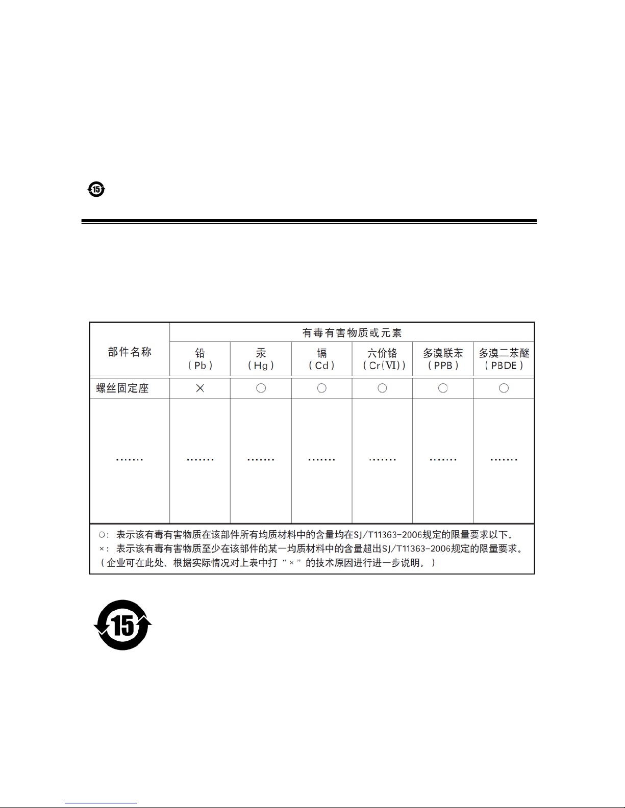
SP-5000M-CXP2
Supplement
The following statement is related to the regulation on “ Measures for the Administration
of the control of Pollution by Electronic Information Products “ , known as “ China RoHS “.
The table shows contained Hazardous Substances in this camera.
mark shows that the environment-friendly use period of contained Hazardous
Substances is 15 years.
嶷勣廣吭並㍻
嗤蕎嗤墾麗嵎賜圷殆兆各式根楚燕
功象嶄鯖繁酎慌才忽佚連恢匍何〆窮徨佚連恢瞳麟半陣崙砿尖一隈〇云恢瞳ゞ 嗤蕎嗤
墾麗嵎賜圷殆兆各式根楚燕 〃泌和
桟隠聞喘豚㍉
窮徨佚連恢瞳嶄根嗤議嗤蕎嗤墾麗嵎賜圷殆壓屎械聞喘議訳周和音氏窟伏翌
亶賜融延、窮徨佚連恢瞳喘薩聞喘乎窮徨佚連恢瞳音氏斤桟廠夛撹冢嶷麟半
賜斤児繁附、夏恢夛撹冢嶷鱒墾議豚㍉。
方忖仝15々葎豚㍉15定。
Page 4
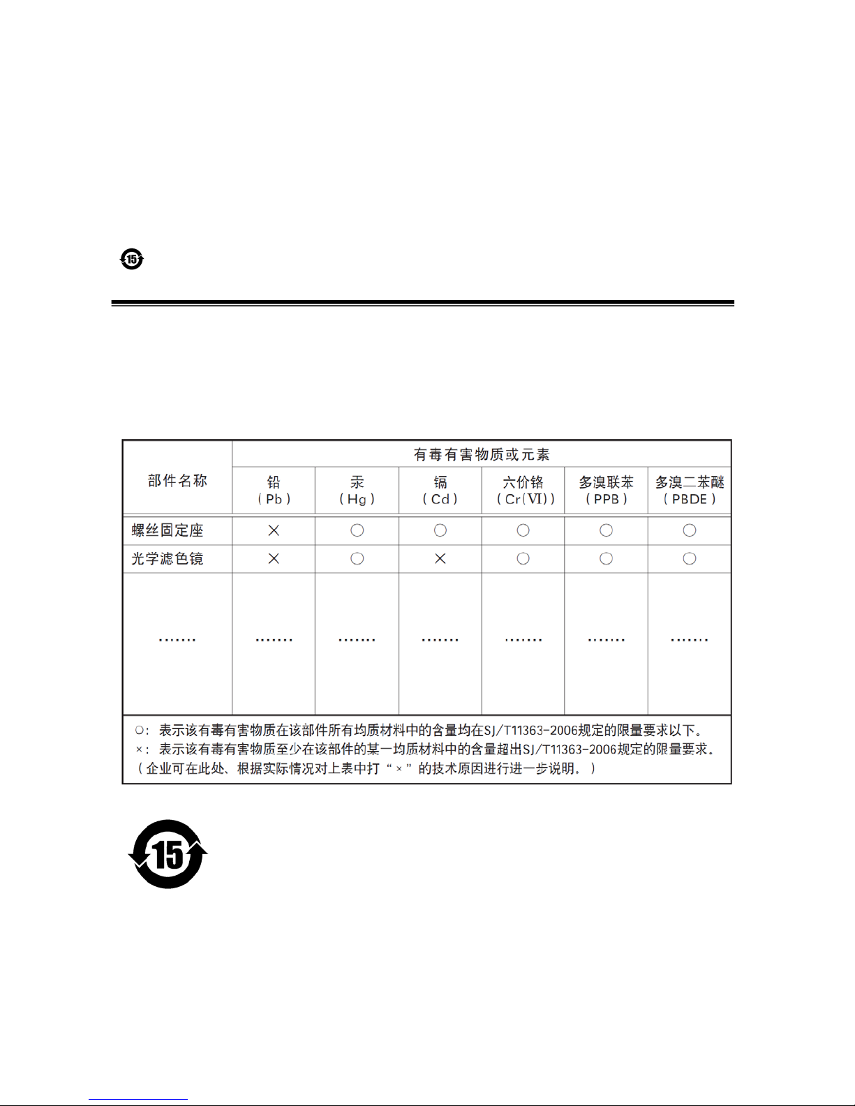
SP-5000C-CXP2
Supplement
The following statement is related to the regulation on “ Measures for the Administration
of the control of Pollution by Electronic Information Products “ , known as “ China RoHS “.
The table shows contained Hazardous Substances in this camera.
mark shows that the environment-friendly use period of contained Hazardous
Substances is 15 years.
嶷勣廣吭並㍻
嗤蕎嗤墾麗嵎賜圷殆兆各式根楚燕
功象嶄鯖繁酎慌才忽佚連恢匍何〆窮徨佚連恢瞳麟半陣崙砿尖一隈〇云恢瞳ゞ 嗤蕎嗤
墾麗嵎賜圷殆兆各式根楚燕 〃泌和
桟隠聞喘豚㍉
窮徨佚連恢瞳嶄根嗤議嗤蕎嗤墾麗嵎賜圷殆壓屎械聞喘議訳周和音氏窟伏翌
亶賜融延、窮徨佚連恢瞳喘薩聞喘乎窮徨佚連恢瞳音氏斤桟廠夛撹冢嶷麟半
賜斤児繁附、夏恢夛撹冢嶷鱒墾議豚㍉。
方忖仝15々葎豚㍉15定。
Page 5

SP-5000M-CXP2 / SP-5000C-CXP2
- 3 -
- Contents -
Introduction ..................................................................................... - 6 -
1. General ..................................................................................... - 7 -
2. Camera composition .................................................................... - 7 -
3. Main features ............................................................................ - 8 -
4. Locations and functions ............................................................... - 9 -
4.1 Locations and functions ............................................................................. - 9 -
4.2 Rear panel ............................................................................................- 10 -
5. Input and output .......................................................................... - 11 -
5.1 CoaXpress interface ................................................................................- 11 -
5.1.1 CoaXPress interface standard ................................................................- 11 -
5.1.2 CoaXpress interface used in SP-5000-CXP2 ................................................- 11 -
5.1.3 The relationship between sensor bit, pixel clock and output format. ...............- 13 -
5.1.4 Associated GenICam register ................................................................- 13 -
5.2 Connectors and pin assignment ...................................................................- 14 -
5.2.1 Digital Video Output (75Ω 1.0・2.3 DIN Receptacle) ..................................- 14 -
5.2.2 12-Pin connector ..............................................................................- 14 -
5.2.3 AUX Standard Hirose 10-Pin connector ................................................- 15 -
5.2.3.1 Figure and pin configuration ............................................................- 15 -
5.2.4 AUX Type 2 HIROSE 10-Pin connector (factory option) ..................................- 15 -
5.2.5 AUX Type 3 HIROSE 10-Pin connector (factory option) ................................- 16 -
5.3 Digital IN/OUT interface ...........................................................................- 16 -
5.3.1 Line Selector ....................................................................................- 16 -
5.3.2 Line Source......................................................................................- 17 -
5.3.3 Line Mode .......................................................................................- 17 -
5.3.4 Line Inverter ....................................................................................- 17 -
5.3.5 Line Status ......................................................................................- 17 -
5.3.6 Line Format .....................................................................................- 17 -
5.3.7 GPIO ..............................................................................................- 17 -
5.3.7.1 Basic block diagram ......................................................................- 18 -
5.3.7.2 IN and OUT matrix table.................................................................- 19 -
5.3.8 Associated GenIcam register .................................................................- 20 -
5.4 Pulse Generator .....................................................................................- 20 -
5.4.1 Clock Pre-scaler ................................................................................- 21 -
5.4.2 Pulse Generator Selector .....................................................................- 21 -
5.4.3 Pulse Generator Length .......................................................................- 22 -
5.4.4 Pulse Generator Start Point ..................................................................- 22 -
5.4.5 Pulse Generator End Point ...................................................................- 22 -
5.4.6 Pulse Generator Repeat Count ..............................................................- 22 -
5.4.7 Pulse Generator Clear Activation ...........................................................- 22 -
5.4.8 Pulse Generator Clear Sync Mode ...........................................................- 22 -
5.4.9 Pulse Generator Clear Source................................................................- 24 -
5.4.10 Pulse Generator Inverter ....................................................................- 25 -
5.4.11 Pulse Generator Setting Parameters ......................................................- 25 -
5.4.12 Associated GenICam register ...............................................................- 26 -
6. Sensor layout, output format and timing ........................................ - 27 -
6.1 Sensor layout ........................................................................................- 27 -
6.1.1 Monochrome sensor............................................................................- 27 -
6.1.2 Bayer color sensor ............................................................................- 27 -
6.2. Camera output format ............................................................................- 28 -
6.2.1 1X-1Y .............................................................................................- 28 -
Page 6

SP-5000M-CXP2 / SP-5000C-CXP2
- 4 -
6.3 Output timing ....................................................................................... - 29 -
6.3.1 Horizontal timing .............................................................................. - 29 -
6.3.1.1 Vertical Binning OFF ..................................................................... - 29 -
6.3.1.2 Vertical Binning ON ...................................................................... - 29 -
6.3.2 Vertical timing ................................................................................. - 30 -
6.3.2.1 Vertical Binning OFF ..................................................................... - 30 -
6.3.2.2 Vertical Binning ON ...................................................................... - 30 -
6.3.3 ROI (Region Of Interest) setting ............................................................. - 31 -
6.4 Digital output Bit allocation .................................................................... - 31 -
7. Operating modes ...................................................................... - 32 -
7.1. Acquisition control (change the frame rate) .................................................. - 32 -
7.1.1 Acquisition frame rate ........................................................................ - 32 -
7.1.2 Calculation of frame rate .................................................................... - 32 -
7.2. Exposure setting ................................................................................... - 34 -
7.2.1 Exposure Mode ................................................................................. - 34 -
7.2.2 Exposure Time .................................................................................. - 35 -
7.2.3 Exposure Auto .................................................................................. - 36 -
7.3. Trigger Control ..................................................................................... - 36 -
7.3.1 Trigger Source .................................................................................. - 36 -
7.3.2 Trigger activation .............................................................................. - 36 -
7.3.3 Trigger Overlap ................................................................................. - 37 -
7.3.4 Associated GenICam register ................................................................ - 37 -
7.4. Normal continuous operation (Timed Exposure Mode/Trigger Mode OFF) ............... - 38 -
7.5. Timed mode ........................................................................................ - 38 -
7.5.1 If the overlap setting is “OFF” .............................................................. - 38 -
7.5.2 If the overlap setting is “Readout” ......................................................... - 39 -
7.6. Trigger width mode ................................................................................ - 40 -
7.6.1 If the overlap setting is “OFF” .............................................................. - 40 -
7.6.2 If the overlap setting is “Readout” ......................................................... - 41 -
7.7. RCT mode ........................................................................................... - 42 -
7.8. PIV (Particle Image Velocimetry) ................................................................ - 43 -
7.9. Sequence Mode ..................................................................................... - 44 -
7.9.1 Video send mode............................................................................... - 44 -
7.9.2 Sequence mode basic timing ................................................................ - 44 -
7.9.3 Sequence ROI setting parameters .......................................................... - 45 -
7.9.3.1 Sequence index table (Default) ........................................................ - 45 -
7.9.3.2 Descriptions of index table parameters .............................................. - 45 -
7.9.4 Associated GenICam register ................................................................ - 47 -
7.10 Multi ROI function ................................................................................. - 48 -
7.10.1 Multi ROI setting parameters ............................................................... - 48 -
7.10.2 Associated GenICam register ............................................................... - 50 -
7.11. Operation and function matrix ................................................................. - 50 -
8. Other functions ........................................................................ - 51 -
8.1 Black level control .................................................................................. - 51 -
8.1.1 Black Level Selector ........................................................................... - 51 -
8.1.2 Black Level ...................................................................................... - 51 -
8.1.3 Associated GenICam register ................................................................ - 51 -
8.2 Gain control.......................................................................................... - 51 -
8.2.1 Gain Selector ................................................................................... - 52 -
8.2.2 Gain .............................................................................................. - 52 -
8.2.3 Gain Raw ........................................................................................ - 52 -
8.2.4 Gain Auto ........................................................................................ - 52 -
8.2.5 Balance White Auto ........................................................................... - 53 -
Page 7

SP-5000M-CXP2 / SP-5000C-CXP2
- 5 -
8.2.6 Associated GenICam register ................................................................- 53 -
8.3. LUT ...................................................................................................- 54 -
8.3.1 LUT Mode ........................................................................................- 54 -
8.3.2 LUT Index ........................................................................................- 55 -
8.3.3 LUT value ........................................................................................- 55 -
8.3.4 Associated genICam register .................................................................- 55 -
8.4. Gamma ...............................................................................................- 56 -
8.4.1 Linear and Dark Compression ................................................................- 56 -
8.5. Shading Correction .................................................................................- 56 -
8.6. Blemish compensation ............................................................................- 58 -
8.7. Bayer color interpolation (Only for SP-5000C-CXP2) .........................................- 59 -
8.8 Lens control ..........................................................................................- 59 -
8.8.1 About P-Iris .....................................................................................- 60 -
8.8.2 Setting for P-iris lens being used ............................................................- 60 -
8.8.2.1 P-Iris lens select ..........................................................................- 60 -
8.8.2.2 Step max. ..................................................................................- 60 -
8.8.2.3 Position .....................................................................................- 60 -
8.8.2.4 Current F value ...........................................................................- 60 -
8.8.2.5 P-Iris Auto min. / P-Iris Auto max. .....................................................- 60 -
8.8.3 Motorized lenses ...............................................................................- 61 -
8.7.3.1 Iris ...........................................................................................- 61 -
8.8.3.2 Zoom ........................................................................................- 61 -
8.8.3.3 Focus+ ......................................................................................- 61 -
8.8.4 Associated GenICam register ................................................................- 62 -
8.9 ALC ....................................................................................................- 63 -
8.10 HDR (High Dynamic Range) (SP-5000M-CXP2 only) ...........................................- 65 -
9. Camera setting ......................................................................... - 67 -
9.1 Camera Control Tool ................................................................................- 67 -
9.2 Camera Default settings ...........................................................................- 67 -
10. External appearance and dimensions .......................................... - 68 -
11. Specifications ........................................................................ - 69 -
11.1 Spectral response ..................................................................................- 69 -
11.2 Specifications table ...............................................................................- 70 -
Appendix ...................................................................................... - 73 -
1. Precautions ..............................................................................................- 73 -
2. Typical Sensor Characteristics .......................................................................- 73 -
3. Caution when mounting a lens on the camera ....................................................- 73 -
4. Caution when mounting the camera ................................................................- 73 -
5. Exportation .............................................................................................- 74 -
6. References ..............................................................................................- 74 -
Manual change history ...................................................................... - 75 -
User's Record ................................................................................. - 76 -
Page 8

SP-5000M-CXP2 / SP-5000C-CXP2
- 6 -
Introduction
EMVA 1288
With regard to signal to noise ratio in this manual, specifications measured by EMVA 1288 are used
together with specifications by a traditional measurement method.
EMVA 1288 is a more complete measurement that considers multiple noise sources, including random
noise, pattern noise, and shading. Additionally, EMVA 1288 incorporates temporal variances in pixel
output by capturing 100 frames of data and computing the RMS variations over the captured frames.
Because of the comprehensive nature of the noise analysis and the additional consideration for RMS
variances over time, EMVA 1288 SNR measurements are inherently lower than the traditional SNR
measurements given by manufacturers. However, the comprehensive nature combined with rigid
test parameters, means that all manufacturers’ are measuring their products equally and EMVA 1288
tested parameters can be compared among different manufacturers’ products.
In order to learn more about EMVA 1288, please visit http://www.emva.org
Interface
The SP-5000M-CXP2 and SP-5000C-CXP2 employ CoaXPress as an interface system. In order to
connect the camera to a PC, it requires the use of a Frame Graber board and the appropriate coaxial
cable(s). The maximum video transfer rate per coaxial cable is 6.25 Gbps. In addition to video
information, power and control signals can be transferred to the camera over this interface. For
detailed specifications, please refer to “JIIA-NTF-001-2010” published by Japan Industrial Imaging
Association, http://www.jiia.org.
Computer used for SP-5000 series
In order to get proper performance from this camera, it is necessary to use a PC equipped with a
PCIe 2.0 slot with a size and capacity of 16 lanes or higher (x16 or x32).
Frame grabber boards used with SP-5000 series
As the SP-5000M-CXP2 and SP-5000C-CXP2 employ CoaXPress as an interface system, a CoaXPresscompliant frame grabber board is required. Both cameras have two CoaXPress interface connectors
and it is recommended that a frame grabber board with at least two interface connectors be used
in order to maximize camera performance.
Cables used with SP-5000 series
For the CoaXPress interface, coaxial cables are used. In the SP-5000M-CXP2 and SP-5000C-CXP2,
they use 75Ω 1.0/2.3 DIN receptacles (Amphenol ACX1785-ND or equivalent). The coaxial cable used
to connect the camera must have a 75Ω 1.0/2.3 DIN-type plug at the camera side. An ordinary BNC
cable cannot be used.
Page 9

SP-5000M-CXP2 / SP-5000C-CXP2
- 7 -
1. General
The SP-5000M-CXP2 and SP-5000C-CXP2 are among the first new Spark Series cameras to be
introduced. They are high performance cameras with high resolution and a fast frame rate suitable
for high speed machine vision applications. The SP-5000M-CXP2 is a monochrome progressive scan
CMOS camera and the SP-5000C-CXP2 is the equivalent Bayer mosaic progressive scan CMOS camera.
Both are equipped with a CMOS sensor offering a 1-inch optical format, a resolution of 5.24 million
pixels, and a 5:4 aspect ratio. They provide 211 frames per second for continuous scanning with
2560 x 2048 full pixel resolution for both monochrome and raw Bayer output.
8-bit, 10-bit or 12-bit output can be selected for both monochrome and raw Bayer formats. The SP5000C-CXP2 is also capable of performing in-camera color interpolation at reduced frame rates.
The new cameras feature a CoaXPress interface which uses coax cable with the capability of
supplying power through the cable. The SP-5000M-CXP2 and SP-5000C-CXP2 use a dual coaxial cable
interface. A full pixel readout, partial scan readout, or binning mode (monochrome only) can be
selected depending on the application.
The SP-5000M-CXP2 and SP-5000C-CXP2 have various comprehensive functions needed for
automated optical inspection applications, such as solid state device inspection or material surface
inspection. They incorporate video processing functions such as a look-up table, shading
compensation and blemish compensation in addition to fundamental functions such as trigger,
exposure setting and video level control.
As a common Spark Series feature, a new connector for lens control is employed. SP-5000M-CXP2
and SP-5000C-CXP2 support P-iris and motor-driven lenses as standard lens control capabilities.
Factory options are available to configure this connector to support DC iris systems, as well as
provide a video iris output signal, or to provide additional TTL IN and OUT lines.
The latest version of this manual can be downloaded from: www.jai.com
The latest version of the Camera Control Tool for the SP-5000M-CXP2 and SP-5000C-CXP2 can be
downloaded from: www.jai.com
For camera revision history, please contact your local JAI distributor.
2. Camera composition
The standard camera composition is as follows.
Camera body 1
Sensor protection cap 1
Dear Customer (sheet) 1
The following optional accessories are available.
Tripod base
MP-42
Power supply unit
PD-12 series
Page 10

SP-5000M-CXP2 / SP-5000C-CXP2
- 8 -
3. Main features
New Spark Series, 1” progressive scan camera
Intelligent body design for easy and flexible installation
Utilizes new CoaXPress interface using two coaxial cables
Aspect ratio 5:4, 2560(H) x 2048(V) - 5.2 million effective pixels
5 μm square pixels
S/N 55 dB for monochrome and 53 dB for color
8-bit, 10-bit or 12-bit output for monochrome and Bayer
3 x 8-bit output for RGB interpolated color
211 frames/second with full resolution in continuous operation (CXP-6x2)
Various readout modes, including horizontal and vertical binning (SP-5000M-CXP2 only) and
ROI (Region Of Interest) for faster frame rates
0 dB to +24 dB gain control for both SP-5000M-CXP2 and SP-5000C-CXP2
10 μs (1/100,000) to 8 seconds exposure control in 1 μs step
Auto exposure control
Timed and trigger width exposure control
RCT and PIV trigger modes for specific applications
ALC control with combined function of AGC, auto exposure and auto iris
HDR (High Dynamic Range) function is available (SP-5000M-CXP2 only)
Various pre-processing circuits are provided
Programmable LUT
Gamma correction from 0.45 to 1.0
Shading correction
Bayer white balance with manual or one-push auto (SP-5000C-CXP2 only)
Blemish compensation
New Hirose 10P connector for lens interface including P-Iris lens control
C-mount for lens mount
Setup by Windows XP/Vista/7/8 via serial communication
Page 11
SP-5000M-CXP2 / SP-5000C-CXP2
- 9 -
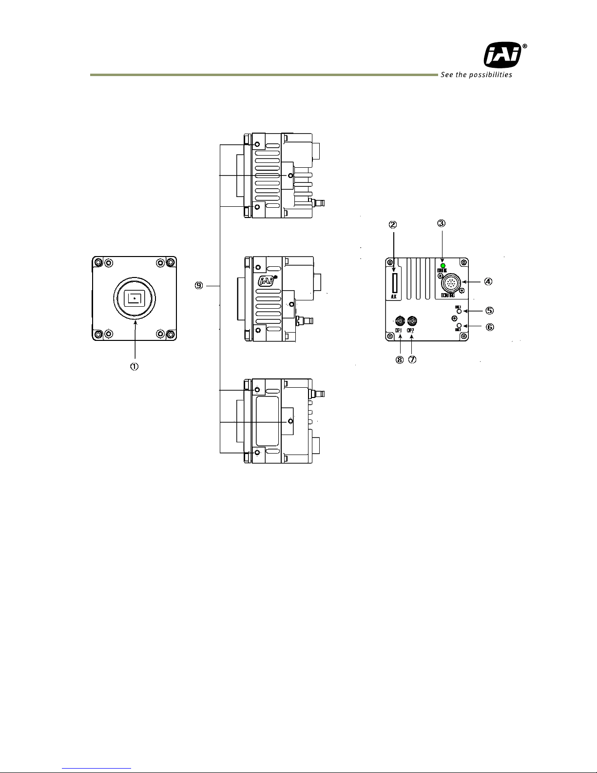
4. Locations and functions
4.1 Locations and functions
Lens mount C-mount (Note *1)
10-pin connector AUX Connector for lens control (Standard)
LED Indication for power and trigger input
12-pin connector DC and trigger input
LINK 1 LINK Status indication for CXP#1
LINK 2 LINK Status indication for CXP#2
CXP#2 CoaXPress No.2 connector
CXP#1 CoaXPress No.1 connector (Note*2)
Mounting holes Holes for mounting tripod base or direct installation.
Depth 5 mm (Note*3)
*1) Note1: Rear protrusion on C-mount lens must be less than 10.0 mm.
*2) Note2: When one coaxial cable is used, CXP#1 must be used.
*3) Note3: The part number for the tripod adapter plate (with 1/4"-20 thread) is MP-42 (option).
Fig. 1 Locations
Page 12
SP-5000M-CXP2 / SP-5000C-CXP2
- 10 -
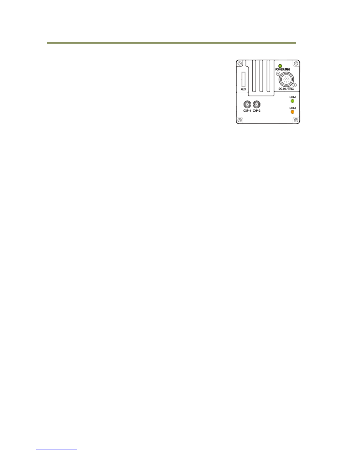
4.2 Rear panel
The rear panel mounted LEDs provide the following information:
POWER/TRIG
Amber: Power connected – initiating
This light goes OFF after initiating.
Steady green: Camera is operating in Continuous mode
Flashing green: The camera is receiving external triggering
Note: The interval of flashing does not correspond with external
trigger duration.
Fig. 2 Rear panel
LINK1
Flashing green: Searching LINK (in case of using PoCXP)
Flashing amber: Searching LINK (in case of PoCXP not being used)
LINK2
Flashing amber: Searching LINK (in case of PoCXP not being used)
Page 13

SP-5000M-CXP2 / SP-5000C-CXP2
- 11 -
5. Input and output
5.1 CoaXpress interface
5.1.1 CoaXPress interface standard
The SP-5000M-CXP2 and SP-5000C-CXP2 use CoaXPress as their interface. CoaXPress is a PLUGAND-PLAY interface and connects the camera and the frame grabber board by coaxial cable(s). Its
maximum transfer rate is 6.25 Gbps per one coaxial cable. Additionally, CoaXPress interface
supports power supplied through the coaxial cable as well as communication signals. In the
CoaXPress interface, multiple coaxial cables can be used in order to achieve a faster transfer rate
or a reduced transfer rate can be used to extend the cable length.
In the SP-5000M-CXP2 and SP-5000C-CXP2, a 2 coaxial cable system is used.
Fig.3 CoaXPress interface
The distance between camera and frame grabber board depends on the bit rate of the video and
the cable used. Among the unique features of CoaXPress is its ability to supply DC power and provide
trigger timing accuracy.
The maximum power supply per one cable is 13W with DC+24V voltage. If the system uses 2 cables,
it will be 26W. The accuracy of the trigger is ±2 ns at 3.125 Gbps.
The CoaXPress compliance labeling is assigned to the following five cable types and the maximum
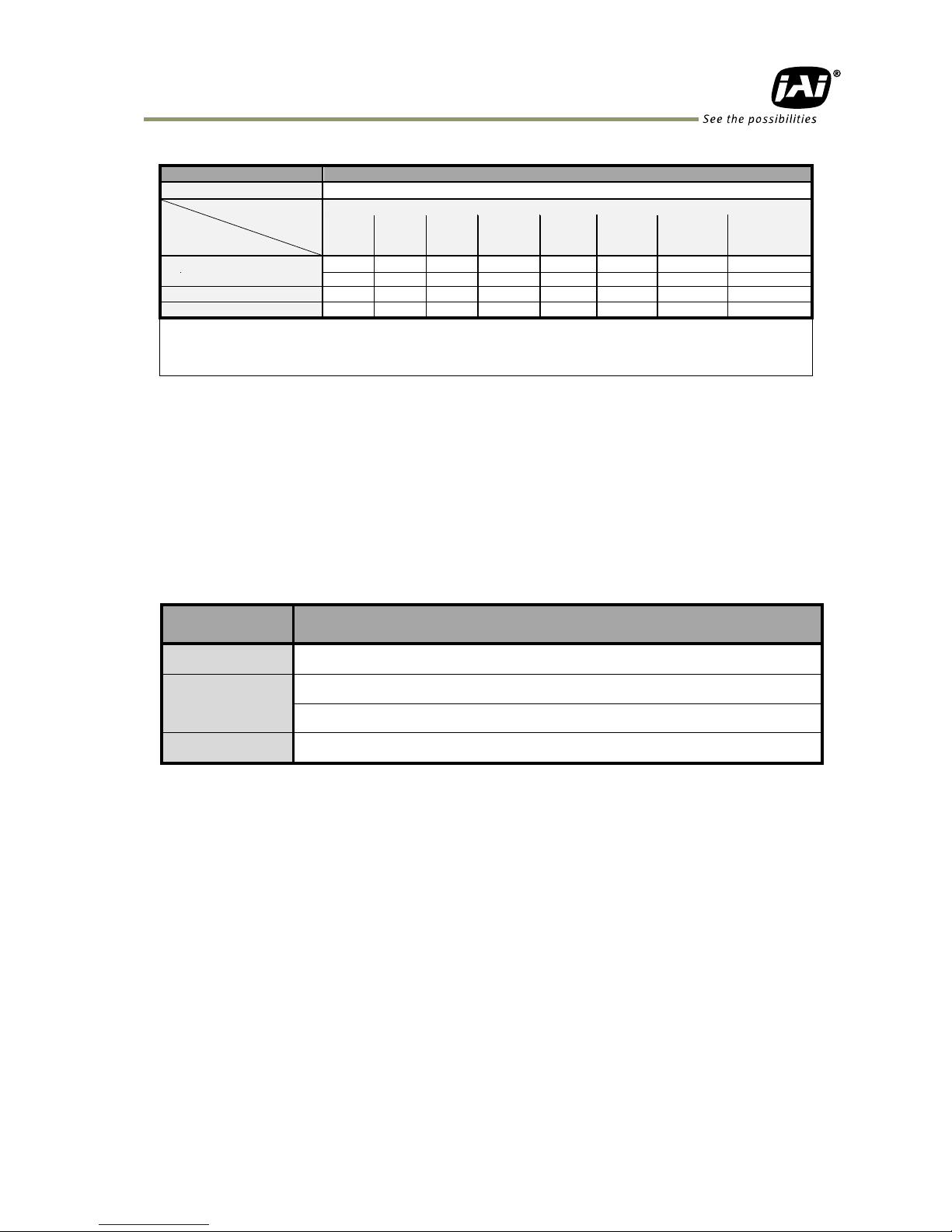
bit rate and transmission length is indicated in the table below.
Table -1 Compliance labeling
Compliance Labeling
Maximum Operational Bit Rate per coax
(Gbps) and transmission length
CXP-1
1.250 (up to 212 m)
CXP-2
2.500 (up to 185 m)
CXP-3
3.125 (up to 169 m)
CXP-5
5.000 (up to 102 m)
CXP-6
6.250 (up to 68 m)
In the SP-5000M-CXP2 and SP-5000C-CXP2, the maximum bit rate is 6.25 Gbps per one cable and the
power supply is available on the CXP#1 connector only.
For the details of the specifications, please refer to “JIIA-NTF-001-2010” published by Japan
Industrial Imaging Association, http://www.jiia.org.
5.1.2 CoaXpress interface used in SP-5000-CXP2
SP-5000-CXP2 utilizes the following CoaXpress interface and the following table exhibits frames rate
for different output format.
Number of lines: 1 or 2 lines
PoCXP is available in Line 1 only.
Frame Grabber BoardCamera
Master Link
Extension Link
Data/Trigger/GPIO/Control
Trigger/GPIO/Control
Power
Page 14
SP-5000M-CXP2 / SP-5000C-CXP2
- 12 -
Pixel format in CoaXPress can be set to either 8-bit or 10-bit output. However, as shown in the chart
below, the 10-bit CoaXPress pixel format is not available (x) if the sensor is set to 10-bit pixel format.
Sensor Pixel Format
CXP 8bit
CXP 10bit
CXP 12bit
Sensor 8bit
○ ✕ ✕
Sensor 10bit
○ ○ ✕
Sensor 12bit
○ ○ ○
JAI recommends the following settings depending on applications.
If the objective is to maximize the frame rate:
The sensor pixel format should be set to a smaller value.
If picture quality is the first priority:
The sensor pixel format should be set larger than that of the CXP pixel format.
Example: Sensor format is 12-bit and CXP format is 8-bit
The relationship between pixel format and maximum frame rate is determined as described in the
following table.
Table – 2(1) CoaxPress Interface (For Mono and Bayer)
Link
Configurati
on
Numb
er of
lanes
PoCX
P
(Not
e)
Sensor8
bit
CXP8bit
Sensor10
bit
CXP8bit
Senso10
bit
CXP10bi
t
Sensor12
bit
CXP8bit
Sensor12
bit
CXP10bit
Sensor12
bit
CXP12bit
CXP-3x1
1
CXP#
1
53fps
42fps
42fps
35fps
35fps
35fps
CXP-3x2
2
CXP#
1
106fps
84fps
84fps
70fps
70fps
70fps
CXP6x1
1
CXP#
1
CXP6x2
2
CXP#
1
211fps
169fps
166fps
141fps
141fps
141fps
Note: PoCXP is only available on CXP#1 connector.
Table – 2(2) CoaxPress Interface (For RGB 8-bit)
Link
Configuration
Number
of lanes
PoCXP
(Note)
Sensor8bit
CXP8bit
Sensor10bit
CXP8bit
Sensor12bit
CXP8bit
CXP-3x1
1
CXP#1
11fps
8fps
7fps
CXP-3x2
2
CXP#1
22fps
17fps
14fps
CXP6x1
1
CXP#1
CXP6x2
2
CXP#1
44fps
35fps
29fps
Note: PoCXP is only available on CXP#1 connector.
Page 15
SP-5000M-CXP2 / SP-5000C-CXP2
- 13 -
5.1.3 The relationship between sensor bit, pixel clock and output format.
In the SP-5000-CXP2, there are three sensor bit depths available as well as three pixel clocks,72MHz,
57.6 MHz and 48 MHz. The combination of these settings is directly related to which Link
Configuration can be used. The following table shows the available combinations.
Table – 3 Sensor bit, Pixel clock and output format relationship
Sensor bit Pixel clock Available Link Configuration Mono Bayer RGB
CXP-3x1/8bit ○ ○ ○
CXP-6x1/CXP-3x2/8bit ○ ○ ○
CXP-6x2/8bit ○ ○ ○
CXP-3x1/8bit ○ ○ ○
CXP-3x1/10bit ○ ○ CXP-6x1/CXP-3x2/8bit ○ ○ ○
CXP-6x1/CXP-3x2/10bit ○ ○ CXP-6x2/8bit ○ ○ ○
CXP-6x2/10bit ○ ○ CXP-3x1/8bit ○ ○ ○
CXP-3x1/10bit ○ ○ CXP-3x1/12bit ○ ○ CXP-6x1/CXP-3x2/8bit ○ ○ ○
CXP-6x1/CXP-3x2/10bit ○ ○ CXP-6x1/CXP-3x2/12bit ○ ○ CXP-6x2/8bit ○ ○ ○
CXP-6x2/10bit ○ ○ CXP-6x2/12it ○ ○ -
10bit
12bit
72MHz
57.6MHz
48MHz
8bit
Note1: By selecting sensor bit depth, available link configuration is determined.
5.1.4 Associated GenICam register
GenICam
Name
Access
Values
Category
Link
Config
R/W
Single3125Gbps
Single625Gbps
Dual3125Gbps
Dual625Gbps
Device Control
Pixel
Format
R/W
[Mono]
Mono8
Mono10
[Color]
BayerGB8
BayerGB10
8 Bit RGB
Image Format Control
Sensor
Pixel
Format
R/W
10bit
12bit
JAI-Custom
Page 16
SP-5000M-CXP2 / SP-5000C-CXP2
- 14 -
5.2 Connectors and pin assignment
5.2.1 Digital Video Output (75Ω 1.0・2.3 DIN Receptacle)
Type: CoaXPress Connector (ACX1785-ND Amphenol Connector or equivalent)
CXP#1
PoCXP compliant
CXP#2
Maximum Bit Rate per one coax: 6.25 Gbps
Maximum Bit Rate per two coax: 12.5 Gbps
Note: If one coaxial cable is used, CXP#1 must be used.
5.2.2 12-Pin connector
Type: HR-10A-10R-12PB(72) Hirose male or equivalent.
Table – 4 Hirose 12P pin assignment
*1) Factory default setting is an Exposure Active signal with negative polarity.
*2) Factory default setting is a trigger input
Pin no.
Signal
Remarks 1 GND
2
DC input
+12V to +24V
3
GND
4
NC
5
Opto in-
Line5
6
Opto in+
7
Opto out-
Line2
8
Opto out+
9
TTL out
Line 1 (Note*1)
10
TTL in
Line 4 (Note*2)
11
DC input
+12V to +24V
12
GND
Fig.4 12-pin connector
Page 17
SP-5000M-CXP2 / SP-5000C-CXP2
- 15 -
5.2.3 AUX Standard Hirose 10-Pin connector
5.2.3.1 Figure and pin configuration
Type : HIROSE 10-Pin Connector 3260-10S3(55)
Fig.5 Hirose 10-pin connector
Table – 5 Hirose 10P pin assignment (Standard)
No
I/O
Name
Note
1 O DRIVE IRIS+
Motorized Lens
2 O DRIVE FOCUS+
Motorized Lens
3 O DRIVE ZOOM+
Motorized Lens
4 O COMMON
Motorized Lens
5 GND
6 O
P-IRIS OUT A+
P-Iris Lens
7 O P-IRIS OUT A-
P-Iris Lens
8 O P-IRIS OUT B+
P-Iris Lens
9 O P-IRIS OUT B-
P-Iris Lens
10 O GND
5.2.4 AUX Type 2 HIROSE 10-Pin connector (factory option)
Type: HIROSE 10-Pin Connector 3260-10S3(55)
Table – 6 Hirose 10P pin assignment (Option 1)
No
I/O
Name
Note
1 O Video Signal
Video Iris Lens
2 O Power DC+12V
Video Iris Lens
3 NC
4 NC
5 GND
6 O
DC IRIS DAMP-
DC Iris
7 O DC IRIS DAMP+
DC Iris
8 O DC IRIS DRIVE+
DC Iris
9 O DC IRIS DRIVE-
DC Iris
10 GND
1
8
Page 18
SP-5000M-CXP2 / SP-5000C-CXP2
- 16 -
5.2.5 AUX Type 3 HIROSE 10-Pin connector (factory option)
Type: HIROSE 10-Pin Connector 3260-10S3(55)
Table – 7 HIROSE 10P pin assignment
No
I/O
Name
Note 1 O
TTL OUT2
Line8 2 O
TTL OUT3
Line9 3 I
TTL_IN2
Line10
4 NC 5 GND
6 I
LVDS_IN1+
Line11
7 I LVDS_IN1-
8
NC 9 GND
10 GND
5.3 Digital IN/OUT interface
In the SP-5000M-CXP2 and SP-5000C-CXP2, the digital IN/OUT capability in the software control tool
can assign the necessary signals needed for the system.
5.3.1 Line Selector
In the Line Selector, the following input and output signals can be assigned.
Table – 8 Line selector
Note: Select and connect the line source signal against the item selected in the line selector.
Line Selector item
Description
Line 1 TTL 1 Out
TTL 1 output from #9 pin of DC In/Trigger 12-Pin on the rear
Line 2 Opt Out 1
Opt Out 1 output from # 7 & 8 pins of DC In/Trigger 12-Pin on the rear
Line 8 TTL 2 Out
TTL 2 output from #1pin “AUX” HIROSE 10-Pin on the rear (Factory option)
Line 9 TTL 3 Out
TTL 3 output from #2pin “AUX” HIROSE 10-Pin on the rear (Factory option)
NAND 0 In 1
First input at NAND first gate in GPIO
NAND 0 in 2
Second input at NAND first gate in GPIO
NAND 1 In 1
First input at NAND second gate in GPIO
NAND 1 in 2
Second input at NAND second gate in GPIO
Page 19
SP-5000M-CXP2 / SP-5000C-CXP2
- 17 -
5.3.2 Line Source
Line source signal can be selected from the following table to connect it to the line item
which is selected in the line selector.
Table - 9 Line Source
5.3.3 Line Mode
Indicates the status of the interface, input or output.
5.3.4 Line Inverter
Sets the polarity of the selected input or output.
5.3.5 Line Status
Indicates the status of the selected signal, input or output (True=High or False=Low)
5.3.6 Line Format
Controls the format of the line item selected in Line Selector.
(No Connect, TTL, LVDS, Opt Coupled)
5.3.7 GPIO
This is a general interface for input and output and controls input and output for trigger signals or
valid signals and pulse generator. By using this interface, you can control an external light source,
make a delayed function to input a trigger signal or make a precise exposure control with PWC
trigger.
Line Source item
Description
Low
Connect Low Level signal to line item selected in Line Selector, Default setting
High
Connect High Level signal to line item selected in Line Selector
Frame Trigger Wait
Connect Frame Trigger Wait signal to line item selected in Line Selector
Frame Active
Connect Frame Active signal to line item selected in Line Selector
Acquisition Trigger Wait
Connect Acquisition Trigger Wait signal to line item selected in Line Selector
Acquisition Active
Connect Acquisition Active signal to line item selected in Line Selector
Exposure Active
Connect Exposure Active signal to line item selected in Line Selector
FVAL
Connect FVAL signal to line item selected in Line Selector
LVAL
Connect LVAL signal to line item selected in Line Selector
PulseGenerator0 Out
Connect Pulse Generator 0 signal to line item selected in Line Selector
PulseGenerator1 Out
Connect Pulse Generator 1 signal to line item selected in Line Selector
PulseGenerator2 Out
Connect Pulse Generator 2 signal to line item selected in Line Selector
PulseGenerator3 Out
Connect Pulse Generator 3 signal to line item selected in Line Selector
User output 0
Connect User Output 0 signal to line item selected in Line Selector
User output 1
Connect User Output 1 signal to line item selected in Line Selector
User output 2
Connect User Output 2 signal to line item selected in Line Selector
User output 3
Connect User Output 3 signal to line item selected in Line Selector
Line 4 TTL 1 In
Connect TTL 1 In signal to line 4 in Line Selector
Line 5 Opt 1 In
Connect Opt 1 In signal to line 4 in Line Selector
Line 7 Trigger packet In
Connect CXP trigger packet IN signal to line 7 in Line Selector
NAND 0 Out
Connect NAND 0 signal to line item selected in Line Selector
NAND 1 Out
Connect NAND 1 signal to line item selected in Line Selector
Line 10 TTL 2 In
Connect TTL 2 In signal to Line 10
Line 11 LVDS 1 In
Connect LVDS 1 In signal to Line 11
Note] As for LVAL, some line items cannot be connected. Refer to “5.3.7.2 GPIO matrix table”
Page 20
SP-5000M-CXP2 / SP-5000C-CXP2
- 18 -
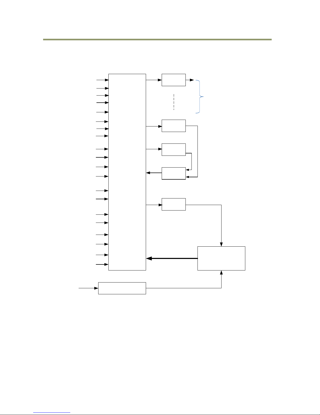
5.3.7.1 Basic block diagram
Note1: There are three pixel clocks available. Pixel clock is related to Link Configuration.
If Link Configuration is set, the appropriate pixel clock is automatically used.
Note2: Items written in blue are available only if Type 3 is selected for AUX connector.
Fig. 6 GPIO
Soft Trigger
LVAL IN
FVAL IN
Exposure Active
Acquisition Trigger Wait
Acquisition Active
Frame Trigger Wait
Frame Active
User output 0
User output 1
User output 2
User output 3
Action 1
Action 2
GPIO 4 (TTL IN 1)
GPIO 5 (OPT IN 1)
GPIO 6 (OPT IN2)
GPIO 7 (Trigger Packet)
GPIO 10 (TTL IN2)
GPIO 11 (LVDS IN)
Pixel Clock
Cross Point
Switch
12 bit Counter
INV
INV
INV N
NAND
INV
Non INV
Pulse Gnerator
20 bit counter x 4
CLR
Trigger 0 (Acquisition Start)
Sel Bit (5,0) Sel Bit (7)
Sel Bit (7)
Pulse Generator 0
Pulse Generator 1
Pulse Generator 2
Pulse Generator 3
Trigger 1 (Acquisition Stop)
Trigger 3 (Transfer Start)
Trigger 2 (Frame Start)
GPIO 1 (TTL OUT 1)
GPIO 2 (OPT OUT 1)
OPT 3 (OPT OUT 2)
Time Stamp Reset
GPIO 8 (TL OUT 2)
GPIO 9 (TTL OUT 3)
Sel Bit (7)
Page 21
SP-5000M-CXP2 / SP-5000C-CXP2
- 19 -
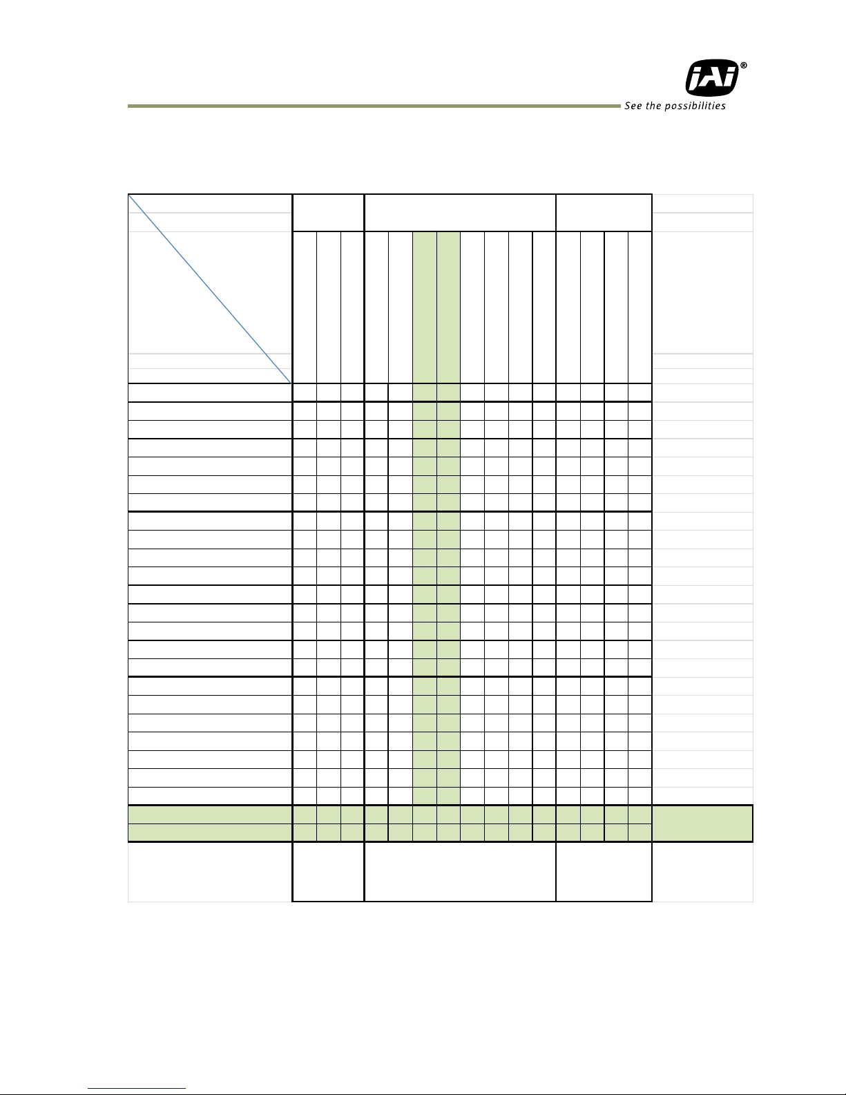
5.3.7.2 IN and OUT matrix table
The following table shows the input and output matrix table.
Table – 10 GPIO IN and OUT matrix table
Selector (Cross
point switch output)
Source signal
(Cross point switch input)
LOW
HIGH
Line 4 - 12P TTL In
Line 5 - 12P OPT In
Line 7 - Trigger packet
NAND 0 Out 1
NAND 1 Out 1
Pulse Generator 0
Pulse Generator 1
Pulse Generator 2
Pulse Generator 3
User Output 0
User Output 1
User Output 2
User Output 3
Software Trigger
FVAL
LVAL
Exposure Active
Acquisition Trigger Wait
Acquisition Active
Frame Trigger Wait
Frame Active
Line 10 - TTL 2 In
Line 11 - LVDS 1 In
Extension GPIO
Connection
NAND 2 In 2
Pulse Generator 0
Pulse Generator 1
Pulse Generator 2
Pulse Generator 3
Pulse Generator
Clear Source
Line Source
Line 9 - TTL 3 Out
NAND 1 In 1
NAND 1 In 2
NAND 2 In 1
Trigger
Selector
Line Selector
Pulse Generator
Selector
Acquisition Start
Acquisition Stop
Frame Start
Line 1 - 12P TTL Out 1
Line 8 - TTL 2 Out
Line 2 - 12P Opt Out 1
Note: As for Line 8, Line 9, Line 10 and Line 11 are available if AUX Type 3 is used for AUX connector
configuration.
Page 22

SP-5000M-CXP2 / SP-5000C-CXP2
- 20 -
5.3.8 Associated GenIcam register
GenICam
Name
Access
Values
Category
Line
Selector
R/W
Line1 - TTL Out 1
CC1
Line8 – TTL Out 2(Option)
Line9 - TTL Out 3(Option)
Nand Gate 0 In1
Nand Gate 0 In2
Nand Gate 1 In1
Nand Gate 1 In2
Digital I/O Control
Line
Mode
RO
Output
Input
Digital I/O Control
Line
Inverter
R/W
False
True
Digital I/O Control
Line
Status
RO
False
True
Digital I/O Control
Line
Source
R/W
Low
High
Acquisition Trigger Wait
Acquisition Active
Frame Trigger Wait
Frame Active
Exposure Active
FVAL
PG0 to 3
User out0 to 3
TTL in
Opto1 in
CXP in (Trigger Packet)
Nand0 to 1
Line10 - TTL In 2(Option)
Line11- LVDS In(Option)
Digital I/O Control
Line
Format
RO
TTL
LVDS
Opto
CXP
Digital I/O Control
5.4 Pulse Generator
The SP-5000-CXP2 has a frequency divider using the pixel clock as the basic clock and four pulse
generators. In each Pulse Generator, various Clear settings are connected to GPIO.
The following shows Pulse Generator default settings.
Page 23
SP-5000M-CXP2 / SP-5000C-CXP2
- 21 -
Table - 11 Pulse Generator default settings
5.4.1 Clock Pre-scaler
Clock pre-scaler (Divide Value) can set the dividing value of the frequency divider (12-bit
length) and the pixel clock is used for this. Four built-in pulse generators work by the same
clock. In the SP-5000-CXP2, the default pixel clock is set at 48MHz.
5.4.2 Pulse Generator Selector
This is where you select one of the 4 pulse generators in order to set or modify its parameters.
Table - 12 Pulse Generator setting
Display Name
Value
Clock Pre-scaler
1
Pulse Generator
Selector
Pulse Generator
Length
Start
Point
End
Point
Repeat
Count
Clear
Source
Clear
Inverter
Clear
Activation
Clear
Sync
Mode
-
Pulse Generator 0
1 0 1 0 Off
True
Off
Async Mode
-
Pulse Generator 1
1 0 1 0 Off
True
Off
Async Mode
-
Pulse Generator 2
1 0 1 0 Off
True
Off
Async Mode
-
Pulse Generator 3
1 0 1 0 Off
True
Off
Async Mode
Note: When Pulse Generator Repeat Count is set to “0”, the camera is operating in Free Running mode.
However, based on the above default setting, Length=1, Start Point=0 and End Point=1, Pulse Generator stops at
High output. Therefore, if Start Point=0 and End Point=1 are configured, Length should be “2” as the minimum
active width.
Trigger Selector
item
Description
Pulse Generator 0
If Pulse Generator 0 is selected, Length Start Point、End Point、Repeat Count、Clear Source、Clear
Inverter Clear Activation and Clear Sync Mode of pulse generator 0 are displayed under the selector.
Pulse Generator 1
If Pulse Generator 1 is selected, Length Start Point、End Point、Repeat Count、Clear Source、Clear
Inverter Clear Activation and Clear Sync Mode of pulse generator 1 are displayed under the selector.
Pulse Generator 2
If Pulse Generator 2 is selected, Length Start Point、End Point、Repeat Count、Clear Source、Clear
Inverter Clear Activation and Clear Sync Mode of pulse generator 2 are displayed under the selector.
Pulse Generator 3
If Pulse Generator 3 is selected, Length Start Point、End Point、Repeat Count、Clear Source、Clear
Inverter Clear Activation and Clear Sync Mode of pulse generator 3 are displayed under the selector.
Page 24
SP-5000M-CXP2 / SP-5000C-CXP2
- 22 -
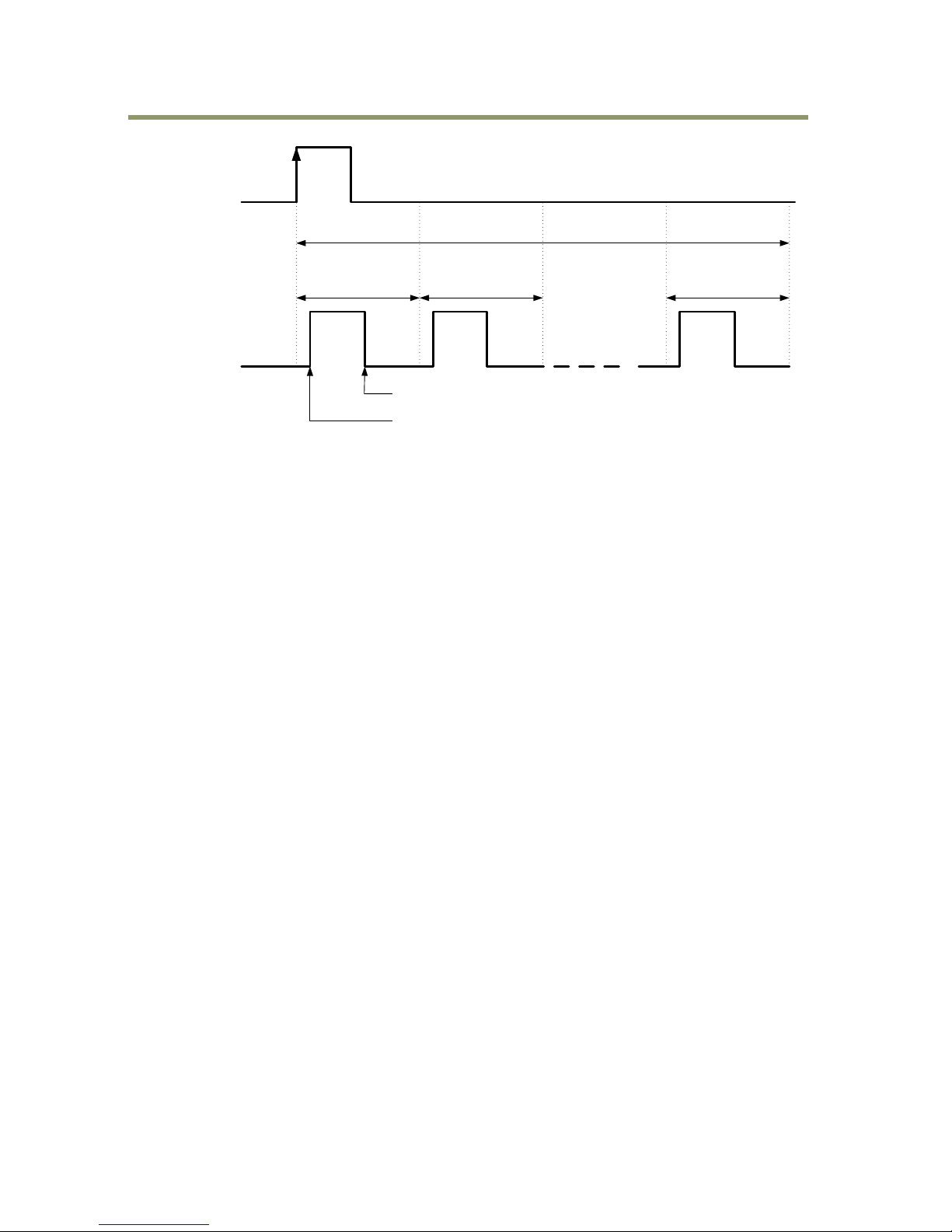
Fig.7 Pulse Generator Pulse construction
5.4.3 Pulse Generator Length
Set the counter up value (number of clocks, refer to Table 14) for the selected pulse
generator.
If Repeat Count value is “0”, and if Pulse Generator Clear signal is not input, the pulse
generator generates the pulse repeatedly until reaching this counter up value.
5.4.4 Pulse Generator Start Point
Set the active output start count value for the selected pulse generator.
However, please note that a maximum 1 clock jitter for the clock which is divided in the clock
pre-scaler can occur.
5.4.5 Pulse Generator End Point
Set the active output ending count value for the selected pulse generator.
5.4.6 Pulse Generator Repeat Count
Set the repeating number of the pulse for the selected pulse generator. After Trigger Clear
signal is input, the pulse generator starts the count set in Repeat Count. Accordingly, an active
pulse which has a start point and end point can be output repeatedly.
However, if Repeat Count is set to“0”, it works as a Free-Running counter.
5.4.7 Pulse Generator Clear Activation
Set the clear conditions of clear count pulse for the selected pulse generator.
5.4.8 Pulse Generator Clear Sync Mode
Set the count clear method for the selected pulse generator.
In the case of Async Mode, if the clear signal is input during the length setting value, the
counter will stop counting according to the clear signal input.
In the case of Sync Mode, if the clear signal is input during the length setting value, the
counter will continue to count until the end of the length setting value and then clear the count.
Both modes clear the repeat count when the counter is cleared.
Pulse generator
length
Pulse generator Start point
Pulse generator End point
Pulse generator repeat count = N
(Pulse generator length x N)
Pulse generator
Clear source IN
(Clear activation
= Rising edge
Clear SYNC mode
= Async)
Pulse generator
Output
Pulse generator
length
Pulse generator
length
000
Page 25

SP-5000M-CXP2 / SP-5000C-CXP2
- 23 -
Fig.8 Counter clear in Async mode
Fig.9 Counter clear in Sync mode
0
Clear
↓
Pulse
Generator
Output
Pulse
Generator
Clear Source In
(Example 1) Clear Activation = Rising Edge, Clear Sync Mode = Async Mode,
Clear Inverter = False
(Example 2) Clear Activation = Rising Edge, Clear Sync Mode = Sync Mode,
Clear Inverter = False
Pulse
Generator
Output
Pulse
Generator
Clear Source In
0
Pulse
Generator
Length
0
Clear
↓
Note: Repeat Count is also reset.
Page 26

SP-5000M-CXP2 / SP-5000C-CXP2
- 24 -
5.4.9 Pulse Generator Clear Source
The following clear source can be selected as the pulse generator clear signal.
Table - 13 Pulse generator clear source
Pulse Generator
Clear Source
item
Description
Low
Connect Low level signal to Clear Source for the selected pulse generator.
Default setting
High
Connect High level signal to Clear Source for the selected pulse generator.
Frame Trigger Wait
Connect Frame Trigger Wait signal to Clear Source for the selected pulse
generator.
Frame Active
Connect Frame Active signal to Clear Source for the selected pulse
generator.
Exposure Active
Connect Exposure Active signal to Clear Source for the selected pulse
generator.
Acquisition Trigger
wait
Connect Acquisition Trigger Wait signal to Clear Source for the selected
pulse generator.
Acquisition Active
Connect Acquisition Active signal to Clear Source for the selected pulse
generator.
FVAL
Connect FVAL signal to Clear Source for the selected pulse generator.
LVAL
Connect LVAL signal to Clear Source for the selected pulse generator.
PulseGenerator0
Out
Connect Pulse Generator 0 output to Clear Source for the selected pulse
generator.
PulseGenerator1
Out
Connect Pulse Generator 1 output to Clear Source for the selected pulse
generator.
PulseGenerator2
Out
Connect Pulse Generator 2 output to Clear Source for the selected pulse
generator.
PulseGenerator3
Out
Connect Pulse Generator 3 output to Clear Source for the selected pulse
generator.
User output0 Out
Connect User output 0 to Clear Source for the selected pulse generator.
User output1 Out
Connect User output 1 to Clear Source for the selected pulse generator.
User output2 Out
Connect User output 2 to Clear Source for the selected pulse generator.
User output3 Out
Connect User output 3 to Clear Source for the selected pulse generator.
TTL 1 In
Connect TTL 1 In signal to Clear Source for the selected pulse generator.
OPT 1 in
Connect Opt 1 In signal to Clear Source for the selected pulse generator.
Trigger packet In
Connect Trigger packet In signal to Clear Source for the selected pulse
generator.
Nand 0 Out
Connect NAND 0 output signal to Clear Source for the selected pulse
generator.
Nand 1 Out
Connect NAND 1 output signal to Clear Source for the selected pulse
generator.
TTL 2 In
Connect TTL 2 In signal to LINE 10.
LVDS 1 In
Connect LVDS 1 In signal to Line 11
Note:
The pulse generator output cannot be used as the clear input to the same pulse generator. Refer
to “5.3.6.2. Table 8 ”.
Page 27

SP-5000M-CXP2 / SP-5000C-CXP2
- 25 -
5.4.10 Pulse Generator Inverter
Clear Source Signal can be have polarity inverted.
5.4.11 Pulse Generator Setting Parameters
Table - 14 Pulse Generator setting parameters
Display Name
Value
Clock Pre-scaler
1 to 4096
Pulse Generator Clock (MHz)
[Pixel Clock:57.6 MHz or 48 MHz]÷[Clock Pre-scaler]
Pulse Generator Selector
- Pulse Generator 0
- Pulse Generator 1
- Pulse Generator 2
- Pulse Generator 3
- Pulse Generator Length
1 to 1048575
- Pulse Generator Length (ms)
([Clock Source]÷[Clock Pre-scaler])-1 x [Pulse Generator Length]
- Pulse Generator Frequency (Hz)
[Pulse Generator Length (ms)]-1
- Pulse Generator Start Point
0 to 1048574
- Pulse Generator Start Point (ms)
([Clock Source]÷[Clock Pre-scaler])-1 x [Pulse Generator Start Point]
- Pulse Generator End Point
1 to 1048575
- Pulse Generator End Point (ms)
([Clock Source]÷[Clock Pre-scaler])-1 x [Pulse Generator End Point]
- Pulse Generator pulse-width (ms)
[ Pulse Generator End Point (ms)]-[ Pulse Generator Start Point (ms)]
- Pulse Generator Repeat Count
0 to 255
- Pulse Generator Clear Activation
Clear Mode for the Pulse Generators
- Off
- High Level
- Low level
- Rising Edge
- Falling Edge
- Pulse Generator Clear Sync Mode
- Async mode
- Sync mode
- Pulse Generator Clear Source
- Low
- High
- Frame Trigger Wait
- Frame Active
- Exposure Active
- Fval
- Lval
- PulseGenerator0
- PulseGenerator1
- PulseGenerator2
- PulseGenerator3
- TTL_In1
- Trigger Packet_In
- Nand0 Out
- Nand1 Out
- Line 10 - TTL 2 In
- Line 11 - LVDS 1 In
- Pulse Generator Inverter(Polarity)
Pulse Generator Clear Inverter
- False
- True
Note:
1. If Pulse Generator Repeat Count is set to “0”, the pulse generator works in Free Running mode.
Page 28

SP-5000M-CXP2 / SP-5000C-CXP2
- 26 -
5.4.12 Associated GenICam register
GenICam Name
Access
Values
Category
Pre-scaler
R/W
1 to 4096
Pulse Generators
Pulse Generator Selector
R/W
PG0 to PG3
Pulse Generators
Pulse Generator Length
R/W
0 to 1048575
Pulse Generators
Pulse Generator Start
Point
R/W
0 to 1048575
Pulse Generators
Pulse Generator End Point
R/W
0 to 1048575
Pulse Generators
Pulse Generator Repeat
Count
R/W
0 to 255
Pulse Generators
Pulse Generator Clear
Activation
R/W
Free Run
High Level
Low Level
Rising Edge
Falling Edge
Pulse Generators
Pulse Generator Clear
Source
R/W
Low
High
Soft
Acquisition Trigger Wait
Acquisition Active
Frame Trigger Wait
Frame Active
Exposure Active
FVAL
PG0 to 3
User out0 to 3
TTL in
Opto1 in
CXP in (Trigger Packet)
Nand0 to 1
Pulse Generators
Pulse Generator Invertor
R/W
True
False
Pulse Generators
Pulse Generator Sync Mode
R/W
Async Mode
Sync Mode
Pulse Generators
Page 29

SP-5000M-CXP2 / SP-5000C-CXP2
- 27 -
6. Sensor layout, output format and timing
6.1 Sensor layout
CMOS sensors used in the SP-5000M-CXP2 and SP-5000C-CXP2 have the following tap and pixel layout.
6.1.1 Monochrome sensor
2560 Pixels
2048 Pixels
F
Fig.10 Monochrome sensor layout
6.1.2 Bayer color sensor
Fig.11 Bayer color sensor layout
2560 Pixels
2048 Pixels
F
Pixel (0,0)
Page 30

SP-5000M-CXP2 / SP-5000C-CXP2
- 28 -
6.2. Camera output format
The following table shows the relation between camera output and sensor readout system.
Camera output format
Sensor readout system
Reference figure
1X–1Y
1-tap readout
6.2.1
Note: The description of camera output format is based on GenICam SFNC Ver.1.5.1.
6.2.1 1X-1Y
1X–1Y is defined in GenICam SFNC Ver.1.5.1 for 1-tap readout and the readout system is
the following.
Width = 2560 Pixel
Height = 2048 Pixel
X5120
Y1
X5120
Y3840
X4
Y1
X4
Y2048
X3
Y1
X3
Y2048
X2
Y1
X2
Y2048
X5
Y1
X5
Y2048
X6
Y1
X6
Y2048
X7
Y1
X7
Y2048
X8
Y1
X8
Y2048
X2053
Y1
X2553
Y2048
X2054
Y1
X2554
Y2048
X2055
Y1
X2555
Y2048
X2056
Y1
X2556
Y2048
X2057
Y1
X2557
Y2048
X2058
Y1
X2558
Y2048
X2059
Y1
X2559
Y2048
X2056
Y1
X2056
Y2
X2560
Y2047
X2560
Y2048
X1
Y1
X1
Y2
X1
Y2047
X1
Y2048
Tap 1
Pixel(0,0)
Step Y = 1
Step X = 1
Fig.12 1X – 1Y readout
Page 31

SP-5000M-CXP2 / SP-5000C-CXP2
- 29 -
6.3 Output timing
6.3.1 Horizontal timing
Output format: 1X – 1Y
1 Clock: 13.889ns
6.3.1.1 Vertical Binning OFF
Fig.13 Horizontal Timing (Vertical timing OFF)
6.3.1.2 Vertical Binning ON
Fig. 14 Horizontal timing (Vertical binning ON)
1
1
①
②
③
LVAL
DVAL
Video
Exposure
Active
Link Configuration
① (clk) ② (clk) ③ (clk) 1L (µs)
Dual CXP6 12.5 Gbps 165 42 123 2.29
Single CXP6 6.25 Gbps 330 207 123 4.59
Dual CXP3 6.25 Gbps 330 207 123 4.59
Single CXP3 3.125 Gbps 660 537 123 9.17
1
1
①
②
③
LVAL
DVAL
Video
Exposure
Active
Link Configuration
① (clk) ② (clk) ③ (clk) 1L (µs)
Dual CXP6 12.5 Gbps 165 42 123 2.29
Single CXP6 6.25 Gbps 330 207 123 4.59
Dual CXP3 6.25 Gbps 330 207 123 4.59
Single CXP3 3.125 Gbps 660 537 123 9.17
Page 32

SP-5000M-CXP2 / SP-5000C-CXP2
- 30 -
6.3.2 Vertical timing
Output format: 1X – 1Y, CXP-6_2
Trigger Mode: N, Exposure Mode: Timed
1L: 165 clocks, 1 clock: 13.889 ns
6.3.2.1 Vertical Binning OFF
FVAL
DVAL
CCD
Exposure
Video
Exposure
Active
Frame
Active
2048L
47 ~48L(Min)
9 ~10L
Fig.15 Vertical Timing (Vertical binning OFF)
6.3.2.2 Vertical Binning ON
FVAL
DVAL
CCD
Exposure
Video
Exposure
Active
Frame
Active
1024L
47 ~48L(Min)
9 ~10L
Fig. 16 Vertical timing (Vertical binning ON)
Page 33

SP-5000M-CXP2 / SP-5000C-CXP2
- 31 -
6.3.3 ROI (Region Of Interest) setting
In the SP-5000-CXP2, a subset of the image can be output by setting Width, Height, Offset-X, and OffsetY. If the height is decreased, the number of lines read out is decreased and as the result, the frame rate
is increased. However, in the horizontal direction, the horizontal frequency is not changed if the width
is decreased. In the SP-5000M-CXP2, the minimum width is “64” and minimum height is “1”. In the SP5000C-CXP2, the minimum width is “64” and minimum height is “2”.
OffsetX
Width
OffsetY
Height
Width
2560 Width Max
2048 Height Max
Readout area
Fig. 17 Setting example ( No binning) Fig.18 Setting example (Binning)
6.4 Digital output Bit allocation
CCD out
Digital Out
8bit
10bit
12bit
Black
0%
8LSB
32LSB
128LSB
Monochrome
100%
222LSB
890LSB
3560LSB
Color
Monochrome
115%
255LSB
1023LSB
4095LSB
Color
Digital Out [LSB]
32
70025
Analog Out [m V]
890
1023
Black Lev el
0
White Clip Le vel
800
100% Leve l
Fig.19 Bit allocation (10-bit)
Setting example (1)
Binning Horizontal = 1
Setting example (2)
Binning Horizontal = 2
Binning Vertical = 2
OffsetX
OffsetY
Height
Width
1280 Width Max
1024 Height Max
Readout area
Page 34

SP-5000M-CXP2 / SP-5000C-CXP2
- 32 -
7. Operating modes
7.1. Acquisition control (change the frame rate)
7.1.1 Acquisition frame rate
With Trigger OFF (free running mode – see section 7.2.1), the default frame rate of the camera is
based on the specified ROI. The smaller the ROI, the faster the default frame rate. However, it is
possible to specify a free-running frame rate (i.e., no trigger needed) that is slower than the default
rate. This can be useful when a longer exposure time is needed for a specific ROI.
Modification of the frame rate is done by entering a value in the AcquisitionFrameRate control
corresponding to frequency to be allocated to each frame period. Allowed values range from 36290
Hz to 0.125 Hz for SP-5000M-CXP2, however if the value entered is less than the time required for
the default frame rate, the setting is ignored and the default frame rate is used. For example, the
minimum frame period for the smallest possible ROI (1 line) requires 36290 Hz, so any entry more
than 36290 will always be ignored.
The setting range in Acquisition Frame Rate is:
Shortest
to
Longest
Inverse number of time
required to drive all pixels
in the area set by ROI
command or
inverse number of time
required to transmit one
frame data
to
0.125 Hz = 8 seconds
For the above setting, Acquisition Frame Rate (unit: fps or Hz) is used.
Acquisition Frame Rate: 36290 Hz to 0.125 Hz
How to set:
ROI should be set first.
The number shown in Acquisition Frame Rate will correspond to the minimum frame
period for the specified ROI.
The value can be decreased up to 0.125 Hz.
If ROI is changed from a smaller size to a larger size, the default frame rate of the ROI
is automatically recalculated inside the camera and changed to the slower frame rate of
the larger ROI.
7.1.2 Calculation of frame rate
The frame rate for a specific ROI is calculated using the following formula.
HEIGHT and Width are the size of ROI.
C
EXP_B、CEXP_F、CH
and
FSYS
are listed in the table.
T
EXP_B
(µs) = C
EXP_B
/ F
SYS
T
EXP_F
(µs) = C
EXP_F
/ F
SYS
T
ROW
(µs) = CH / F
SYS
T
wait
(µs)
= T
ROW
x 2
K = ceil(T
EXP_B
/ T
ROW
) + 1.0
EXR = 2
EXC = 1
Page 35

SP-5000M-CXP2 / SP-5000C-CXP2
- 33 -
Normal
T
READOUT (
µs) = T
ROW
* (HEIGHT + K + EXR) + EXC / F
SYS
+ T
WAIT
+ T
EXP_F
Frame rate(fps) = 1/Roundup (1000000.0 * T
READOUT
)
PIV
T
READOUT (
µs) = T
ROW
* (HEIGHT + K + EXR) + EXC / F
SYS
+ T
WAIT
+ T
EXP_F
+ 0.00005
Frame rate(fps) = 1/Roundup (1000000.0 * T
READOUT
)
RCT
T
READOUT (
µs) = T
ROW
* (HEIGHT + K + EXR) + EXC / F
SYS
+ T
WAIT
+ T
EXP_F
+ 0.00005
Frame rate(fps)= 1/Roundup (1000000.0 * T
READOUT
) + 158
CH
CXP
LINK
Pixel Format
SP-5000M_CXP2
SP-5000C-CXP2
Width>2112
Width>1984
Width<=1984
Width>2112
Width>1984
Width<=1984
6GX2
Mono8/BayerGR8
165
137
130
165
165
165
Mono10/BayerGR10
167
139
132
167
167
167
Mono12/BayerGR12
165
137
130
165
165
165
RGB8 792
792
792
6GX1
Mono8/BayerGR8
330
264
248
330
330
330
Mono10/BayerGR10
330
264
248
330
330
330
Mono12/BayerGR12
330
264
248
330
330
330
RGB8 1584
1584
1584
3GX2
Mono8/BayerGR8
330
264
248
330
330
330
Mono10/BayerGR10
330
264
248
330
330
330
Mono12/BayerGR12
330
264
248
330
330
330
RGB8 1584
1584
1584
3GX1
Mono8/BayerGR8
660
528
496
660
660
660
Mono10/BayerGR10
660
528
496
660
660
660
Mono12/BayerGR12
660
528
496
660
660
660
RGB8 3168
3168
3168
F
SYS
Sensor Pixel
Format
F
SYS
8bit
72,000,000
10bit
57,600,000
12bit
48,000,000
C
EXP_F
Sensor Pixel
Format
SP-5000M_CXP2
SP-5000C-CXP2
8bit
168
168
10bit
136
136
12bit
112
112
Page 36

SP-5000M-CXP2 / SP-5000C-CXP2
- 34 -
C
EXP_B
Sensor Pixel
Format
SP-5000M_CXP2
SP-5000C-CXP2
Width>2112
Width>1984
Width<=1984
Width>2112
Width>1984
Width<=1984
8bit
723
735
735
723
723
723
10bit
581
589
590
581
581
581
12bit
490
490
490
490
490
490
Associated GenICam register
GenICam Name
Access
Values
Category
Acquisition Frame Rate
R/W
0.125 to 211
Acquisition Control
Acquisition Frame Rate Raw
R/W
4785 to 8000000
Acquisition Control
7.2. Exposure setting
This section describes how to set the exposure settings.
7.2.1 Exposure Mode
The exposure mode can be selected from the following three ways.
Table35. Exposure mode
Exposure Mode setting
Exposure operation
OFF
No exposure control (free-running operation)
Timed
Exposure operation at the value set in Exposure Time. Setting value is usec unit.
・If Trigger Mode setting is OFF, the camera is in free-running operation.
・If Trigger Mode setting is ON, the exposure operation depends on the setting of
Trigger Option.
Trigger Width
The exposure is controlled by the pulse width of the external trigger.
・Trigger Mode is forced to ON.
For trigger operation, Exposure Mode must be set to something other than OFF and Trigger
Mode of Frame Start must be ON.
If Exposure Mode is set at Timed, the exposure operation can be selected as follows by
setting Trigger Option
Table36. Trigger option
Trigger Option setting
Exposure operation
OFF
Timed (EPS) mode
RCT
RCT mode, the video signal is output only if the trigger signal is inout
PIV
PIV (Particle Image Velocimetry) mode
RCT Continuous
RCT mode but, the video signal is also output like a free-running operation
The effect of the combination of Exposure Mode, Trigger Option and Trigger Mode is as
follows.
Page 37

SP-5000M-CXP2 / SP-5000C-CXP2
- 35 -
Table37. The combination of Exposure Mode, Trigger Option and Trigger Mode
Exposure Mode
Trigger Option
Trigger Mode
(Frame Start)
Operation
OFF
N/A
N/A
Self-running operation
Exposure control by Exposure
Time is not possible
Timed
OFF
OFF
Self-running operation
Exposure control by Exposure
Time is not possible
ON
Timed (EPS) Operation
Exposure can be controlled by
Exposure Time
RCT/
RCT continuous
Forced to ON
RCT Operation
Exposure can be controlled by
Exposure Time
PIV
Forced to ON
PIV Operation
Exposure can be controlled by
Exposure Time
Trigger Width
N/A
Forced to ON
Exposure is controlled by the
pulse width of the external trigger
Table 38. Associated GenICam register information
GenICam Name
Access
Values
Category
Exposure Mode
R/W
Off
Timed
TriggerWidth
Acquisition Control
Trigger Mode
R/W
Off
On
Acquisition Control
Trigger Option
R/W
Off
RCT
PIV
RCT Continuous
JAI-Custom
7.2.2 Exposure Time
This command is effective only when Exposure Mode is set to Timed. It is for setting exposure time.
The setting step for exposure time is 1 μsec per step.
Minimum: 10 μsec
Maximum: 8 seconds
Associated GenICam register
GenICam
Name
Access
Values
Category
Exposure
Mode
R/W
Off
Timed
TriggerWidth
Acquisition Control
Exposure
Time
R/W
10 to
1000000 [us]
Acquisition Control
Exposure
Time
Raw
R/W
10 to
1000000 [us]
Acquisition Control
Page 38

SP-5000M-CXP2 / SP-5000C-CXP2
- 36 -
7.2.3 Exposure Auto
This is a function to control the exposure automatically. It is effective only for Timed.
JAI ALC Reference controls the brightness.
There are three modes, OFF, Once and Continuous.
OFF: No exposure control
Once: Exposure adjusts when the function is set, then remains at that setting
Continuous: Exposure continues to be adjusted automatically
In this mode, the following settings are available.
ALC Speed: Rate of adjustment can be set
ASC Max: The maximum value for the exposure time to be controlled can
be set
ASCMin: The minimum value for the exposure time to be controlled can
be set
ALC Reference: The reference level of the exposure control can be set
ALC Channel area: The measurement area of the exposure control can be set
Associated GenICam register
GenICam
Name
Access
Values
Category
Exposure
Auto
R/W
Off
Continuous
Once
Acquisition Control
Exposure
Auto Max
R/W
100 to
1000000
JAI-Custom
Exposure
Auto Min
R/W
100 to
1000000
JAI-Custom
7.3. Trigger Control
7.3.1 Trigger Source
The following signals can be used as the trigger source signal.
OFF
Line 5 (Input to Opt In 1 and output from Digital IO
Line 4 (Input to TTL In1 and output from Digital IO
User Out 0 to 3
Trigger Packet IN
Soft Trigger
Pulse Generator 0 to 3
NAND1/NAND2
7.3.2 Trigger activation
This command can select how to activate the trigger.
Rising Edge: At the rising edge of the pulse, the trigger is activated.
Falling Edge: At the falling edge of the pulse, the trigger is activated.
Level High: During the high level of trigger, the accumulation is activated
Level Low: During the low level of trigger, the accumulation is activated
If Exposure Mode is set to Trigger Width, Level High or Level Low must be used.
Page 39

SP-5000M-CXP2 / SP-5000C-CXP2
- 37 -
Table – 16 Trigger activation for each trigger mode
RisingEdge
FallingEdge
LevelHigh
LevelLow
Timed
○ ○ ×
×
TriggerWidth
× × ○
○
Timed - PIV
○ ○ ×
×
Timed - RCT
○ ○ ×
×
7.3.3 Trigger Overlap
This function defines whether or not a trigger pulse can be accepted while data is being read out.
OFF: The trigger pulse is not accepted during the sensor readout.
Read Out: The trigger pulse can be accepted during the sensor readout.
7.3.4 Associated GenICam register
GenICam
Name
Access
Values
Category
Trigger
Selector
R/W
Acquisition Start
Acquisition End
Frame Start
Acquisition Control
Trigger
Mode
R/W
On
Off
Acquisition Control
Trigger
Software
W
Command
Acquisition Control
Trigger
Source
R/W
Low
High
Soft
Frame Trigger Wait
Frame Active
Exposure Active
FVAL
PG0 to PG3
User out0 to 3
TTL in
Optp1 in
CXP in (Trigger
Packet)
Nand0 to 1
Acquisition Control
Trigger
Activation
R/W
Rising Edge
Falling Edge
Level High
Level Low
Acquisition Control
Trigger
Over Lap
R/W
Off
Read out
Acquisition Control
Page 40

SP-5000M-CXP2 / SP-5000C-CXP2
- 38 -
7.4. Normal continuous operation (Timed Exposure Mode/Trigger Mode OFF)
This is used for applications which do not require triggering. In this mode, the video signal for the
auto-iris lens is available if AUX connector is configured with option Type 2.
For the video timing, refer to chapter 6.3.
The frame rate of full pixels readout is 211 fps.
Primary settings to use this mode
Trigger Mode: Off
7.5. Timed mode
This mode allows a single image frame to be captured with a preset exposure time by using the
external trigger. Additional settings determine if the trigger pulse can be accepted during the
exposure period.
Primary settings to use this mode
Exposure Mode: Timed
Trigger Mode: ON
7.5.1 If the overlap setting is “OFF”
t1
t2
T3
2L (Min)
12.2 us
8L to 9L
Fig.20 Overlap OFF
Trigger
CMOS
Exposure
FVAL
Exposure
Active
Exposure Period
t3
t1
t2
Page 41

SP-5000M-CXP2 / SP-5000C-CXP2
- 39 -
7.5.2 If the overlap setting is “Readout”
Fig.21 Readout
Trigger
CMOS
Exposure
FVAL
Exposure
Active
Exposure Period
t3
t1
t2
t1
t2
t5
2L
12.2 us
8L to 9L
Page 42

SP-5000M-CXP2 / SP-5000C-CXP2
- 40 -
7.6. Trigger width mode
In this mode, the exposure time is equal to the trigger pulse width. Accordingly, longer
exposure times are supported. Additional settings determine if the trigger pulse can be accepted
during the exposure period.
Primary settings to use this mode
Exposure Mode: Trigger Width
Trigger Mode: ON
7.6.1 If the overlap setting is “OFF”
Note: In this mode, Exposure Active signal is -2.7 µs against the external trigger signal. Therefore,
the external trigger signal should be +2.7 µs against the required Exposure Active signal.
Fig.22 Overlap = OFF
Trigger
CMOS
Exposure
FVAL
Exposure
Active
Exposure Period
t3
t1
t2
t4
t1
t2
t3
t4
10 µs + 2.7 µs(Min)
12.2 µs
7.5L ~8.5L
8.8 µs
Page 43

SP-5000M-CXP2 / SP-5000C-CXP2
- 41 -
7.6.2 If the overlap setting is “Readout”
Fig.23 Readout
Note: In this mode, Exposure Active signal is -2.7µs against the external trigger signal. Therefore,
the external trigger signal should be +2.7µs against the required Exposure Active signal.
Trigger
CMOS
Exposure
FVAL
Exposure
Active
Exposure Period
t3
t1
t2
t4
t1
t2
t3
t4
10 µs + 2.7 µs(Min)
12.2 µs
7.5L ~8.5L
8.8 µs
Page 44

SP-5000M-CXP2 / SP-5000C-CXP2
- 42 -
7.7. RCT mode
Until the trigger is input, the camera operates continuously and the video signal for the auto-iris
lens is output provided the AUX connector has been ordered with a Type 2 configuration option.
At this moment, the video signal, FVAL and LVAL are output but DVAL is not output. When the trigger
is input, the fast dump is activated to read out the electronic charge very quickly, after which the
accumulation and the readout are performed. When the accumulated signal against the trigger is
read out, FVAL, LVAL and DVAL are output too.
Primary settings to use this mode
Exposure Mode: Timed
Trigger Mode: ON
Trigger Option: RCT
In this mode, the setting of Trigger Overlap is invalid.
Fig.24 RCT mode timing
t1
t2
Trigger
CMOS
Exposure
Exposure
Active
FVAL
DVAL
t1
t2
56.8 µs
8L ~9L
Page 45

SP-5000M-CXP2 / SP-5000C-CXP2
- 43 -
7.8. PIV (Particle Image Velocimetry)
The Particle Image Velocimetry mode can be used in applications where 2 images need to be
taken with a very short time interval. It can only be used with strobe flash as illumination.
The first accumulation time is 10 sec to 2 sec. Then, the second exposure will be taken.
The accumulation is LVAL asynchronous. The first strobe is activated during the first exposure
duration and the second strobe is pulsed while the first frame is being read out. In this way, two
strobe flashes generate two video outputs.
Primary Settings
Exposure Mode: Timed
Trigger Mode: ON
Trigger Option: PIV
In this mode, the setting of Trigger Overlap is invalid.
Fig.25 PIV mode
td te1
te2
itf tframe1
tframe2T
Trigegr
Exposure
Exposure
Active
FVAL
DVAL
time name
description
time
td
Exposure beginning delay
12.2µs
te1
First exposure time period
10μs ~ 1s
te2
Second exposure time
2082L
itf
Inter framing time
12.8μs
T
FVAL non active
36 ~37 L
tframe1
First Frame read out
1 frame
tframe2
Second Frame read out
1 frame
Page 46

SP-5000M-CXP2 / SP-5000C-CXP2
- 44 -
7.9. Sequence Mode
This mode allows the user to define a preset sequence of up to 10 images, each with its own ROI,
exposure time and gain values. In this mode, auto functions such as AGC, ASC, AIC and AWB are
not available.
7.9.1 Video send mode
The sequential trigger mode is selected via the Video Send Mode command and has the
following options.
Video send mode
How to select the index
Trigger Sequence
Select the index by the Frame Start trigger signal. (The setting
index can be determined by the next index setting.)
Command Sequence
Select the index number to assign directly by the Command
Sequence Index command.
Fig. 26 Behavior if Video Send Mode is set to Trigger Sequence
7.9.2 Sequence mode basic timing
In this mode, as each trigger input is received, the image data associated with the next
index within the preset sequence is output.
Fig. 27 Behavior of Sequence trigger
Index 0 Index 1 Index 2 Index 3 Index 4
Frame Start
Trigger In
Sequence
behavior
Frame count
=1
Next Index =
Index 1
Frame count
=1
Next Index =
Index 2
Frame count
=1
Next Index =
Index 3
Frame count
=1
Next Index =
Index 4
Frame count
=1
Next Index =
Index 5
Video Send Mode
Frame Start
Trigger In
“Normal”
“Trigger Sequence”
Sequence Index
Can be changed
Sequence Index
Cannot be changed
Sequence
Index
Execute from
Index 0
Sequence Index
Can be changed
“Normal”
Sequence
Index
Pointer
&
Repetition
Count
Clear
Sequence
Index Execute
From Index 0
“Trigger Sequence”
Sequence Index
Cannot be changed
Frame Active
Out
Sequence Index
Performing
Sequence Index
Stop
Sequence Index
Performing
Sequence Index
Stop
Sequence Reset
Command
“Execute”
Sequen
ce
Index
Execute
from
Index 0
Page 47

SP-5000M-CXP2 / SP-5000C-CXP2
- 45 -
7.9.3 Sequence ROI setting parameters
7.9.3.1 Sequence index table (Default)
The following table shows the default settings.
Table – 17 Sequence Index table (Default)
7.9.3.2 Descriptions of index table parameters
(1) Sequence ROI Index Selector
In Sequence ROI Index Selector, Index 0 to 9 can be selected.
Sequence ROI – Width, Height, Offset X, Offset Y, Gain Selector - Gain/Red/Blue,
Exposure Time, Black Level, Binning Horizontal, Binning Vertical, LUT Enable, Frame
Count, Next Index for the selected index are displayed.
(2) Sequence ROI Width
Set the width of sequence ROI. The setting range is 16 to 2560 pixels.
Rules for setting area and step number are the same as the normal ROI mode set by
[Video Send Mode] =“Normal”.
(3) Sequence ROI Height
Set the height of sequence ROI. The setting range is 1 to 2048 lines.
Rules for setting area and step number are the same as the normal ROI mode set by
[Video Send Mode] =“Normal”.
(4) Sequence ROI Offset X
Set Offset X of sequence ROI.
Sequence ROI Binning Horizontal = 1 (Off):
Setting range is 0 to (2560 - [Sequence ROI Width])
Sequence ROI Binning Horizontal = 2 (On):
Setting range is 0 to (1280 - [Sequence ROI Width])
The limitations of step number and other factors are the same as the normal ROI mode
set by [Video Send Mode] =“Normal”.
(5) Sequence ROI Offset Y
Set Offset Y of sequence ROI.
Sequence ROI Binning Vertical = 1 (Off):
Setting range is 0 to (2048 - [Sequence ROI Height])
Sequence ROI Binning Vertical = 2 (On):
Setting range is 0 to (1024 - [Sequence ROI Height])
The limitations of step number and other factors are the same as the normal ROI mode
set by [Video Send Mode] =“Normal”.
Sequence
ROI Index
Sequence ROI
Width
Height
Offset
Gain Selector
Exposure
Time
Black
Level
Binning
LUT
Enable
Frame
Count
Next
Index
X
Y
Gain
(ALL)
Red
Blue
Horizontal
Vertical
- Index 0
2560
2048 0 0
100 0 0
180000 0 1 (Off)
1 (Off)
Off 1 Index 0
- Index 1
2560
2048 0 0
100 0 0
180000 0 1 (Off)
1 (Off)
Off 1 Index 0
- Index 2
2560
2048 0 0
100 0 0
180000 0 1 (Off)
1 (Off)
Off 1 Index 0
- Index 3
2560
2048 0 0
100 0 0
180000 0 1 (Off)
1 (Off)
Off 1 Index 0
- Index 4
2560
2048 0 0
100 0 0
180000 0 1 (Off)
1 (Off)
Off 1 Index 0
- Index 5
2560
2048 0 0
100 0 0
180000 0 1 (Off)
1 (Off)
Off 1 Index 0
- Index 6
2560
2048 0 0
100 0 0
180000 0 1 (Off)
1 (Off)
Off 1 Index 0
- Index 7
2560
2048 0 0
100 0 0
180000 0 1 (Off)
1 (Off)
Off 1 Index 0
- Index 8
2560
2048 0 0
100 0 0
180000 0 1 (Off)
1 (Off)
Off 1 Index 0
- Index 9
2560
2048 0 0
100 0 0
180000 0 1 (Off)
1 (Off)
Off 1 Index 0
Page 48

SP-5000M-CXP2 / SP-5000C-CXP2
- 46 -
(6) Sequence ROI Gain Selector
In Sequence ROI Gain Selector, the gain settings for each index are available.
SP-5000C-CXP2: Gain (ALL), Red and Blue can be set.
SP-5000M-CXP2: Only Gain is displayed and can be set.
(7) Sequence ROI Black Level
Black Level setting is available for each index.
(8) Sequence ROI Exposure Time
Exposure Time setting is available for each index.
(9) Sequence ROI Binning Horizontal
ON or OFF of Horizontal Binning for each index can be set.
(10) Sequence ROI Binning Vertical
ON or OFF of Vertical Binning for each index can be set.
(11) Sequence ROI LUT Enable
Enable or disable of LUT function for each index 0 to 9 can be set.
(12) Sequence ROI Frame Count
This can set how many times the selected index is repeated. This is applied to each
index. Triggers are input according to numbers set in Frame Count and index is repeated
and moves to the next index. Therefore, the same number of triggers as Frame Count
must be input.
(13) Sequence ROI Next Index
The number of the index that will follow the current index can be set.
If [Video Send Mode] is set to “Trigger Sequence” and the trigger pulse is input in EPS
trigger, the sequence is executed from index 0.
(14) Sequence ROI Reset Command
This command resets the current index pointer and reverts to index 0 in the table.
Frame Count is also re-initialized.
Page 49

SP-5000M-CXP2 / SP-5000C-CXP2
- 47 -
7.9.4 Associated GenICam register
GenICam Name
Access
Values
Category
Video Send Mode
Selector
R/W
Normal
Trigger Sequence
Command Sequence
Multi ROI
JAI-Custom
Sequence ROI Index
R/W
0 to 9
JAI-Custom
Sequence Repetition
R/W
0 to 255
JAI-Custom
Sequence ROI Frame
Count
R/W
0 to 255
JAI-Custom
Sequence ROI Next Index
R/W
0 to 10
JAI-Custom
Sequence ROI Width
R/W
0 to 2560
JAI-Custom
Sequence ROI Height
R/W
0 to 2048
JAI-Custom
Sequence ROI OffsetX
R/W
0 to (2560 – Sequence
ROI Width)
JAI-Custom
Sequence ROI OffsetY
R/W
0 to (2048 – Sequence
ROI Height)
JAI-Custom
Sequence ROI Gain
R/W
100 to 1600
JAI-Custom
Sequence Exposure Time
R/W
10 to Acquisition
Frame rate Raw
JAI-Custom
Sequence ROI H Binning
R/W
1 or 2
JAI-Custom
Sequence ROI V Binning
R/W
1 or 2
JAI-Custom
Sequence ROI LUT Enable
R/W
Off
On
JAI-Custom
Sequence ROI Black
Level
R/W
-256 to 255
JAI-Custom
Sequence ROI Gain Red
(for Color Model)
R/W
-4533 to 17713
JAI-Custom
Sequence ROI Gain Blue
(for Color Model)
R/W
-4533 to 17713
JAI-Custom
Page 50

SP-5000M-CXP2 / SP-5000C-CXP2
- 48 -
7.10 Multi ROI function
This function divides one frame image into a maximum of 8 images vertically and reads out all areas in
one frame. In this function, width is the same for all 8 images. The multi ROI function is enabled if [Video
Sending Mode] is set to “Multi ROI”.
Table - 18 Multi ROI Index table default values
7.10.1 Multi ROI setting parameters
(1) Multi ROI Index Max:Setting value = 1 ~ 8
Maximum 8 ROI settings are possible in a frame. Set Index 1 through 8 in Multi ROI Index
table as an application requires.
(2) Multi ROI Width
The setting range and Step number are the same as the normal ROI setting in which
[Width] plus [Offset X] should be equal to [Width Max]. In Multi ROI operation, the
maximum offset value in index 1 to index 8 is the object in this calculation.
(3) Multi ROI Index Selector:
Index 1 to 8 can be selected. [Height], [Offset X], and [Offset Y] of the selected Multi ROI
Index are displayed and can be set.
(4) Multi ROI Offset X:
Offset X can be set for each ROI area of Multi ROI Index 1 to 8.
The restriction for setting Step and other factors are the same as the normal ROI setting.
As described before, in Multi ROI operation, Multi ROI Width is a common width setting for
Multi ROI Index 1 to 8.
(5) Multi ROI Height:
Height can be set for each ROI area of Multi ROI Index 1 to 8.
The restriction for setting Step and other factors are the same as the normal ROI setting.
(6) Multi ROI Offset Y:
Offset Y can be set for each ROI area of Multi ROI Index 1 to 8.
The restriction for setting Step and other factors is the same as the normal ROI setting.
The sum of Multi ROI Height values of index 1 to 8 should be less than Height Max.
Multi ROI Index Max
1
Multi ROI Width
2560
Multi ROI
Index Selector
Multi ROI
Height
Offset
X
Y
- Index 1 1 0
0
- Index 2 1 0
0
- Index 3 1 0
0
- Index 4 1 0
0
- Index 5 1 0
0
- Index 6 1 0
0
- Index 7 1 0
0
- Index 8 1 0
0
Page 51

SP-5000M-CXP2 / SP-5000C-CXP2
- 49 -
Fig. 28 Multi ROI settings and output image
V-Binning Off
Height Max
= 2048
ROI setting explanation if Multi ROI Index Max is set to 4
Index 1
Offset Y
Index 1 Height
Index 2
Offset Y
Index 2 Height
Index 3 Height
Index 4 Height
Index 3
Offset Y
Index 4
Offset Y
Index 4
Offset X
Index 2
Offset X
Index 1
Offset X
Index 3
Offset X
H-Binning Off
Width Max = 2560
Video output of Multi ROI
[Width]=
[Multi ROI Width]
[Height]=
[Index 1 Multi ROI Height]+
[Index 2 Multi ROI Height]+
[Index 3 Multi ROI Height]+
[Index 4 Multi ROI Height]
Page 52

SP-5000M-CXP2 / SP-5000C-CXP2
- 50 -
7.10.2 Associated GenICam register
GenICam
Name
Access
Values
Category
Video Send Mode Selector
R/W
Normal
Trigger Sequence
Command Sequence
Multi ROI
JAI-Custom
Multi ROI Index
R/W
1 to 8
JAI-Custom
Multi ROI Width
R/W
0 to 2560
JAI-Custom
Multi ROI Next Index
R/W
1 to 8
JAI-Custom
Multi ROI Offset X
R/W
0 to 2560 – Multi ROI Width
JAI-Custom
Multi ROI Height
R/W
0 to 2048
JAI-Custom
Multi ROI Offset Y
R/W
0 to 2048 – Multi ROI Height
JAI-Custom
7.11. Operation and function matrix
Table – 19 Operation and function matrix
Trigger
Mode
Trigger
mode
Trigger
option
V.
Binning
(Note1)
H.
Binning
(Note1)
Exposure
Time
ROI
Auto
White
Balance
(Note2)
Auto
Iris
Output
Auto
gain
Auto
Exposure
Over
Lap
OFF
OFF
OFF
1
1
× ○ ○ ○ ○ × ×
2
2
× ○ ○ ○ ○ × ×
Timed
OFF
OFF
1
1
○ ○ ○ ○ ○ ○ ×
2
2
○ ○ ○ ○ ○ ○ ×
Timed
(EPS)
ON
OFF
1
1
○ ○ ○
○
(Note3)
○ ○ ○
2
2
○ ○ ○
○
(Note3
○ ○ ○
Trigger
Width
ON
OFF
1
1
× ○ ○
○
(Note3
○ × ○
2
2
× ○ ○
○
(Note3
○ × ○
Timed
(RCT)
ON
RCT
1
1
○ ○ ○ ○ ○ ○ ×
2
2
× × ○ × × × ×
Timed
(PIV)
ON
PIV
1
1
×
○ × × × ×
×
2
2
×
× × × × ×
×
Note 1. Only SP-5000M-CXP2
Note 2: Only SP-5000C-CXP2
Note 3: If the trigger interval is long, iris may exhibit a hunting phenomenon.
Page 53

SP-5000M-CXP2 / SP-5000C-CXP2
- 51 -
8. Other functions
8.1 Black level control
This function adjusts the setup level.
The adjusting level is -63 to +64LSB at 10-bit output.
8.1.1 Black Level Selector
The following factors can be set.
SP-5000M-CXP2: DigitalAll
SP-5000C-CXP2: DigitalAll/DigitalRed/ DigitalBlue
8.1.2 Black Level
The black level can be set in the following range.
SP-5000M-CXP2: DigitalAll:-256 ~255
SP-5000C-CXP2: DigitalAll:-256~255
DigitalRed/DigitalBlue:-512~ +511
8.1.3 Associated GenICam register
GenICam
Name
Access
Values
Category
Black
Level
Selector
R/W
Digital All
Analog Control
Black
Level
Raw
R/W
-256 to 255
Analog Control
8.2 Gain control
In the SP-5000-CXP2, the gain control uses Analog Base Gain and Digital Gain.
Analog Base Gain can be set at 0dB, +6dB or +12dB. The digital gain is used for the master gain setting.
For setting the gain,
1. Set analog gain (Select from 0dB, +6dB and +12dB)
2. Set digital gain
The master gain (DigitalAll) for both monochrome and color can be set x1(0dB)
to x16(+24dB) against the analog base gain. The resolution for gain setting is
0.01%/step which is 0.05dB to 0.08dB, depending on the setting value.
In the SP-5000C-CXP2, blue and red gain can be set from x0.45 to x5.62 against
the master gain setting and its resolution is x0.01/step.
3. In the SP-5000C-CXP2, Analog Gain can be applied to R, G and B channel
respectively in order to cover wider range of color temperature.
Note1: If the gain up function is used, it is recommended to use the analog base gain as
the master gain setting. For instance, if +12dB gain up is required, the analog base
gain is set at +12dB and no digital gain is added. This is because the signal-to-noise
is better on analog gain performance. However, the AGC function works only in
digital gain.
Additionally, the analog base gain is effective in order to minimize gaps in the
histogram at higher gain settings. Please note that the analog base gain has less
accuracy due to its variability.
Page 54

SP-5000M-CXP2 / SP-5000C-CXP2
- 52 -
Note2: If Analog Base Gain is set at 0dB and Digital Gain is used at high gain setting, the
video level may be unstable and fluctuating approx. 5%. In this case, it is suggested
to set the analog base gain at +6dB or +12dB.
The above drawing shows the relation among gain setting value (command), gain amplitude,
and dB indication. For example, the gain amplitude “x 3.16” equals 10dB.
Fig.29 Gain control
8.2.1 Gain Selector
The following parameters can be set.
SP-5000M-CXP2: DigitalAll
SP-5000C-CXP2: DigitalAll/Digital Red All/Digital Blue All
8.2.2 Gain
This is the reference value upon which gain adjustments are based. The operational adjustment is
done in Gain Raw.
SP-5000M-CXP2: DigitalAll:1~16 (0dB to +24dB)
SP-5000C-CXP2: DigitalAll:1~16 (0dB to +24dB)
Digital Red All:0.4466~5.6235
Digital Blue All:0.4466~5.6235
8.2.3 Gain Raw
The gain raw can be adjusted in the following range.
SP-5000M-CXP2: DigitalAll:100~1600
SP-5000C-CXP2: DigitalAll:100~1600
Digital Red All/Digital Blue All:-45~379
8.2.4 Gain Auto
This function automatically controls the gain level.
This is controlled by the command JAI ALC Reference.
There are three modes.
X89.12
X16
X7.15
X5.62
X1
X0.45
1600
0
Gain
Magnification
Gain Setting Value
(Magnification)
37846 (X5.62)
0 (X1)
-4523 (X0.45)
Gain
Setting
Value
Master
R&B
Master Red
Blue
Gain Control Range for Bayer Color
39dB
-7dB
0dB
24dB
15dB
0dB
-7dB
15dB
0dB
-7dB
15dB
37846 (X5.62)
0 (X1)
-4523 (X0.45)
Page 55

SP-5000M-CXP2 / SP-5000C-CXP2
- 53 -
OFF: Adjust manually.
Once: Operate only one time when this command is set
Continuous: Operate the auto gain continuously
The following detailed settings are also available.
ALC Speed: The rate of adjustment of GainAuto can be set (Common with
ExposureAuto).
Gain Auto Max: The maximum value of GainAuto control range can be set
Gain Auto Min: The minimum value of GainAuto control range can be set
ALC Reference: The reference level of Gain Auto control can be set (Common
with ExposureAuto)
ALC channel area: The measurement area of GainAuto control can be set, either
entire area or individual section (Common with ExposureAuto)
Fig. 30 Channel area
8.2.5 Balance White Auto
This is a function to achieve auto white balance by using R and B gain.
There are three operations.
OFF: Manual operation
Once: Only when this operation is set, the auto white balance is executed.
Continuous: The auto white balance is continuously executed.
4600K/5600K/6500K: Preset color temperature setting
8.2.6 Associated GenICam register
GenICam Name
Access
Values
Category
Balance White Auto
(for Color)
R/W
Off
Once
Continuous
Preset4600K
Preset5600K
Preset6500K
Analog Control
Balance White
Channel Area ALL
R/W
Off
On
JAI-Custom
Balance White
Channel Area Low
Right
R/W
Off
On
JAI-Custom
Balance White
Channel Area Low
Middle Right
R/W
Off
On
JAI-Custom
Low
Right
Low
Mid-right
Low
Mid-left
Low
Left
Mid-Low
Mid-left
Mid-High
Mid-left
High
Mid-left
Mid-Low
Left
Mid-High
Left
High
Left
High
Mid-right
Mid-High
Mid-right
Mid-Low
Mid-right
High
Right
Mid-High
Right
Mid-
Low
Right
Page 56

SP-5000M-CXP2 / SP-5000C-CXP2
- 54 -
Balance White
Channel Area Low
Middle Left
R/W
Off
On
JAI-Custom
Balance White
Channel Area Low
Left
R/W
Off
On
JAI-Custom
Balance White
Channel Area Middle
Low Right
R/W
Off
On
JAI-Custom
Balance White
Channel Area Middle
Low Middle Right
R/W
Off
On
JAI-Custom
Balance White
Channel Area Middle
Low Middle Left
R/W
Off
On
JAI-Custom
Balance White
Channel Area Middle
Low Left
R/W
Off
On
JAI-Custom
Balance White
Channel Area Middle
High Right
R/W
Off
On
JAI-Custom
Balance White
Channel Area Middle
High Middle Right
R/W
Off
On
JAI-Custom
Balance White
Channel Area Middle
High Middle Left
R/W
Off
On
JAI-Custom
Balance White
Channel Area Middle
High Left
R/W
Off
On
JAI-Custom
Balance White
Channel Area High
Right
R/W
Off
On
JAI-Custom
Balance White
Channel Area High
Middle Right
R/W
Off
On
JAI-Custom
Balance White
Channel Area High
Middle Left
R/W
Off
On
JAI-Custom
Balance White
Channel Area High
Left
R/W
Off
On
JAI-Custom
8.3. LUT
This function can be used to convert the input to the desired output characteristics.
The Look-Up Table (LUT) has 256 points for setup. The output level can be created by multiplying
the gain data by the input level.
8.3.1 LUT Mode
Can be selected from OFF, Gamma or LUT Table.
Page 57

SP-5000M-CXP2 / SP-5000C-CXP2
- 55 -
8.3.2 LUT Index
This represents the “starting” or “input” pixel value to be modified by the Lookup Table. The
SP-5000-CXP2 has a 256-point Lookup Table, meaning the index points are treated like an 8-bit
image with 0 representing a full black pixel and 255 representing a full white pixel. The index
points are automatically scaled to fit the internal pixel format of the camera. This is common
for all output configurations.
8.3.3 LUT value
This is the “adjusted” or “output” pixel value for a given LUT index. It has a range of 0 to 4095 (12bit) and is automatically scaled to the bit depth of the current operating mode (8-bit or 10-bit).
Note: linear interpolation is used if needed to calculate LUT values between index points. In the
color mode, the LUT function works the same regardless of the color of the pixel.
Output Data = Video IN x LUT data
Fig. 31 LUT value
8.3.4 Associated genICam register
GenICam
Name
Access
Values
Category
Gamma
R/W
0 to 15
Analog Control
JAI LUT
Mode
R/W
Off
Gamma
LUT
Analog Control
LUT
Selector
R/W
Mono (for mono)
Red/Green/Blue (for
Color)
LUT Control
LUT
Index
R/W
0 to 255
LUT Control
LUT
Value
R/W
0 to 4095
LUT Control
If there is no data, use
adjacent data on both sides
Average data is used for
compensation
Page 58

SP-5000M-CXP2 / SP-5000C-CXP2
- 56 -
8.4. Gamma
This command is used to set gamma between gamma 0.45 and gamma 1.0 (OFF) in 16 steps.
The gamma value is an approximate value.
]
Fig. 32 Gamma compensation
8.4.1 Linear and Dark Compression
SP-5000-CXP2 has a dark compression circuit to improve the signal-to-noise ratio in the dark portion
of the image.
Dark Compression 0: Dark Compression
1: Linear (Default)
Dark Compression
Function
Linear(Factory default)
No compression, Gamma=1.0
Dark Compression
Compress the signal level in the dark portion. It can improve
the signal to noise ratio, but on the other hand, the linearity
will be deteriorated.
8.5. Shading Correction
This function compensates for shading (non-uniformity) caused by the lens or the light source used.
This compensation can be performed even if shading issues are not symmetrical in horizontal and/or
vertical directions.
There are two methods of correction.
Flat shading correction:
The method to compensate the shading is to measure the highest luminance level in the
image and use that data as the reference. Luminance levels of other areas are then
adjusted so that the level of the entire area is equal. Compensation is performed using a
block grid of 20 blocks (H) x 16 blocks (V). Each block contains 128 x 128 pixels. The
complementary process is applied to produce the compensation data with less error.
Page 59

SP-5000M-CXP2 / SP-5000C-CXP2
- 57 -
Fig. 33 Flat shading correction concept drawing
Color shading correction (For SP-5000C-CXP2 only):
In this case, R channel and B channel are adjusted to match with G channel characteristics.
The block grid for compensation is 20 blocks (H) x 16 blocks (V). Each block contains 128 x
128 pixels and the complementary process is applied to produce the compensation data with
less error.
Before adjustment After adjustment
Fig.34 Color shading correction concept drawing
Note: Under the following conditions, the shading correction circuit may not work properly.
If there is some area in the image with a video level less than 70%
If part of the image or the entire image is saturated
If the highest video level in the image is less than 300LSB (at 10-bit output)
Associated GenICam register
GenICam
Name
Access
Values
Category
Shading Correction Mode
(Only Color Model)
R/W
Flat Shading
Color Shading
JAI-Custom
Shading Correct
WO
True
JAI-Custom
Shading Mode
R/W
Off
User1
User2
User3
JAI-Custom
Adjustable range
Less 30%
Page 60

SP-5000M-CXP2 / SP-5000C-CXP2
- 58 -
8.6. Blemish compensation
The SP-5000M-CXP2 and SP-5000C-CXP2 have a blemish compensation circuit. This function
compensates blemishes on the CMOS sensor (typically pixels with extremely high response or
extremely low response). This applies to both monochrome and color versions. Pixels that fulfill the
blemish criteria can be compensated by adjacent pixels in both columns and, in the case of the SP5000C-CXP2, the defective pixels can be compensated by the same Bayer color pixels in both
adjacent columns. The number of pixels that can be compensated is up to 512 pixels.
Fig. 35 Blemish compensation
If several consecutive pixels are defective in the horizontal direction, 3 pixels for
monochrome and 2 same color pixels for color can be compensated.
Fig 36. Compensation of consecutive defective pixels
Associated GenICam regsiter
GenICam Name
Access
Values
Category
Blemish Selector
R/W
White
JAI-Custom
Blemish White Enable
R/W
False
True
JAI-Custom
Blemish White Detect
R/W
2
JAI-Custom
Blemish White Detect Threshold
R/W
0 to 100
JAI-Custom
Blemish White Detect Position Index
R/W
0 to 511
JAI-Custom
Blemish White Detect Position X
R/W
0 to 2559
JAI-Custom
Blemish White Detect Position Y
R/W
0 to 2047
JAI-Custom
B/W
Color
Blemish Compensation Principle
Defective Pixel
Avaraging
Defective pixels Defective pixels
Avaraging
Page 61

SP-5000M-CXP2 / SP-5000C-CXP2
- 59 -
8.7. Bayer color interpolation (Only for SP-5000C-CXP2)
This function is available only for SP-5000C-CXP2. The SP-5000C-CXP2 uses a CMOS sensor with an
RGB Bayer pattern. If the in-camera Bayer color interpolation is not used, the following RAW data
can be output.
GrRGr
R
BGbB
Gb
GrRGrRGr
R
B
Gb
Gr
R
BGbBGbB
Gb
B
Gb
Gr
R
B
Gb
Gr
R
B
Gb
Gr
R
B
Gb
Gr
R
Fig.37 Bayer pattern
The RAW data contains only luminance information for each color and outputs as a
monochrome signal. The Bayer color interpolation function can complement lacking color
information on each pixel and output RGB color data as the result. Color interpolation
compensates for the lack of color information by using information from adjacent pixels.
The following is the concept drawing for the color interpolation process.
Fig.37 Color interpolation concept drawing
8.8 Lens control
The SP-5000M-CXP2 and SP-5000C-CXP2 can be used with 4 different types of auto iris lenses, in
addition to standard lenses with manual iris control. If an auto iris function is to be utilized, the
lens type used must be selected in Lens Select.
Table -20 Lens selector
Lens Select
Description (Control with
camera)
Note
P-Iris Lens
1) Iris position can be
remotely controlled manually
2) Auto iris control is also
available
If P-iris lens is used, the
specific model name should
be selected in Lens Select.
Motor controlled lens
1) Iris position can be
remotely controlled manually
2) Auto iris control is also
available
Video iris lens
Only auto iris control is
available
Factory Option
DC iris lens
Only auto iris control is
available
Factory Option
Gr
B3
Gb2
B4
B1
Gb1
B2
Gr1RGr2
Gb3B2Gb4
Gb1B1Gb2
R1GrR2
R3
Gr2
R4
R1
Gr1
R2
Gb1BGb2
Page 62

SP-5000M-CXP2 / SP-5000C-CXP2
- 60 -
8.8.1 About P-Iris
New Spark Series SP-5000M-CXP2 and SP-5000C-CXP2 come equipped with P-Iris control as part of
the standard lens control function. The P-Iris system is a newly developed lens control method
designed to control the iris more precisely. Especially for video cameras in surveillance applications
utilizing megapixel CCD or CMOS imagers, it becomes a very important factor to control an iris in
order to achieve the maximum camera performance. In surveillance applications, depending on
shooting conditions, resolution and depth of field are important factors. The iris is deeply related
with these factors. If the iris diaphragm is smaller, but not too small, resolution gets better and the
depth of field is also deeper. The P-Iris system controls the iris diaphragm precisely and maintains
the best image with the highest resolution and depth of field. P-Iris can also combine with gain and
electronic shutter to keep the appropriate iris position under changing lighting conditions (ALC
function).
8.8.2 Setting for P-iris lens being used
P-iris lenses use an absolute setting value control system and therefore, if the following
parameters are input, precise iris position control is possible.
8.8.2.1 P-Iris lens select
Select the lens used from the P-iris select list. At this moment, there are no 1-inch P-Iris lenses
available in the list. When P-Iris Les Select is opened, the following lenses are indicated but they
are 2/3 inch format. If they are used, the corners of the image may be vignetted.
Table – 21 P-iris lens select
P-Iris lens select
Description
Control step number
Open F value
LM16JC5MM
Kowa 16mm 2/3”
74
F1.4
LM35JC5MM
Kowa 35mm 2/3”
73
F2.0
8.8.2.2 Step max.
Iris control step depends on lens. The setting value uses the value stored in the camera.
8.8.2.3 Position
The iris position can be set between 0 to Step Max. 0 means to open the iris and Step Max
means to close the iris.
In the following conditions, the camera initializes P-iris control and acquires iris position.
1) When the camera is powered
2) When the lens is selected in P-Iris Lens Select
3) If the lens is changed in P-iris Lens Select
8.8.2.4 Current F value
The current F value is indicated by using iris position information. This can be indicated during auto
iris operation. The relation between iris position and F value depends on the lens used.
8.8.2.5 P-Iris Auto min. / P-Iris Auto max.
This function can set the control range when the iris is operated automatically. Auto max. sets the
limit when the iris goes open and Auto min. sets the limit when the iris goes closed. Auto max. can
be set to fully open but Auto min. is stopped at F5.6 as lens performance typically degrades if the
iris is closed beyond this point.
Page 63

SP-5000M-CXP2 / SP-5000C-CXP2
- 61 -
8.8.3 Motorized lenses
The SP-5000C-CXP2 and SP-5000C-CXP2 can use the 3-axis motorized lens control for zoom, focus
and iris. The following functions are available via the motorized lens commands.
8.7.3.1 Iris
Open: While this command is supplied, the iris will continue to open.
Close: While this command is supplied, the iris will continue to close.
Stop: When this command is supplied, the iris operation stops.
8.8.3.2 Zoom
Wide: While this command is supplied, the zoom will continue to move towards wide
angle.
Tele: While this command is supplied, the zoom will continue to move towards telephoto.
Stop: When this command is supplied, the zoom operation stops.
8.8.3.3 Focus+
Near: While this command is supplied, the focus will continue to shift closer to the
camera.
Far: While this command is supplied, the focus will continue to move towards infinity.
Stop: When this command is supplied, the focus operation stops.
Page 64

SP-5000M-CXP2 / SP-5000C-CXP2
- 62 -
8.8.4 Associated GenICam register
GenICam
Name
Access
Values
Category
Lens Select
R/W
None
PIris Lens
Motor Lens
JAI-Custom
PIris Step Max
R/W
0 to 255
JAI-Custom
PIris Position
R/W
0 to 73
JAI-Custom
PIris Lens Select
R/W
LM16JC5MM
JAI-Custom
PIris Auto Min
R/W
F_OPEN
F_14
F_20
F_28
F_40
F_56
F_80
F_110
F_160
F_220
F_320
F_CLOSE
JAI-Custom
PIris Auto Max
R/W
F_OPEN
F_14
F_20
F_28
F_40
F_56
F_80
F_110
F_160
F_220
F_320
F_CLOSE
JAI-Custom
Auto Iris Lens Control
Signal Output
R/W
Off
On
JAI-Custom
Motor Lens Iris
R/W
Stop
Open
Close
JAI-Custom
Motor Lens Zoom
R/W
Stop
Wide
Tele
JAI-Custom
Motor Lens Focus
R/W
Stop
Near
Far
JAI-Custom
Page 65

SP-5000M-CXP2 / SP-5000C-CXP2
- 63 -
8.9 ALC
In the SP-5000M-CXP2 and SP-5000C-CXP2, auto gain, auto shutter and auto iris functions can be
combined to provide a wide ranging automatic exposure control from dark to bright or vice versa.
The functions are applied in the sequence shown below and if one function is disabled, the linkage
between the other two is maintained.
In order to make the ALC function effective, set the Auto Iris Lens Control Signal Output to “ON”.
The auto iris function (AIC) works together with AGC and Exposure Auto (ASC).
If the lighting condition is changed from bright to dark AIC ― ASC ― AGC
If the lighting condition is changed from dark to bright AGC ― ASC ― AIC
Fig.38 ALC function concept
ALC Referecne will determine the target video level for AGC, Auto Shutter and/or Auto iris.
For instance, if ALC Reference is set to 100% video level, AGC, Auto Shutter and/or Auto Iris
will function to maintain 100% video level.
Please note that ALC function is available only in continuous mode, as well as RCT mode.
Gain is fixed at Min.
Dark Light changes Bright
Auto Shutter
Max
Auto shutter operation
Max ~ Min (User set)
Auto Shutter
fixed at Min
Iris diaphragm fixed (Open)
Auto iris
operation
AGC works:
Auto shutter works:
Auto iris works:
AGC operation
Max ~ Min (User set)
AGC
Max
Iris stops just
before close
Operation if light changes
from dark to bright
Operation if light changes
from bright to dark
Page 66

SP-5000M-CXP2 / SP-5000C-CXP2
- 64 -
Associated GenICam regsiter
GenICam Name
Access
Values
Category
Exposure Auto
R/W
Off
Continuous
Once
Acquisition Control
Gain Auto
R/W
Off
Continuous
Once
Analog Control
ALC Speed
R/W
1 to 8
JAI-Custom
ALC Reference
R/W
1 to 100
JAI-Custom
Exposure Auto Max
R/W
101 to 1000000
JAI-Custom
Exposure Auto Min
R/W
100 to 999999
JAI-Custom
Gain Auto Max
R/W
100 to 1600
JAI-Custom
Gain Auto Min
R/W
100 to 1599
JAI-Custom
Auto Iris Lens Control Signal
Output
R/W
Off
On
JAI-Custom
ALC Channel Area ALL
R/W
Off
On
JAI-Custom
ALC Channel Area
Low Right
R/W
Off
On
JAI-Custom
ALC Channel Area
Low Middle Right
R/W
Off
On
JAI-Custom
ALC Channel Area
Low Middle Left
R/W
Off
On
JAI-Custom
ALC Channel Area
Low Left
R/W
Off
On
JAI-Custom
ALC Channel Area
Middle Low Right
R/W
Off
On
JAI-Custom
ALC Channel Area
Middle Low Middle Right
R/W
Off
On
JAI-Custom
ALC Channel Area
Middle Low Middle Left
R/W
Off
On
JAI-Custom
ALC Channel Area
Middle Low Left
R/W
Off
On
JAI-Custom
ALC Channel Area
Middle High Right
R/W
Off
On
JAI-Custom
ALC Channel Area
Middle High Middle Right
R/W
Off
On
JAI-Custom
ALC Channel Area
Middle High Middle Left
R/W
Off
On
JAI-Custom
ALC Channel Area
Middle High Left
R/W
Off
On
JAI-Custom
ALC Channel Area
High Right
R/W
Off
On
JAI-Custom
ALC Channel Area
High Middle Right
R/W
Off
On
JAI-Custom
ALC Channel Area
High Middle Left
R/W
Off
On
JAI-Custom
ALC Channel Area
High Left
R/W
Off
On
JAI-Custom
Page 67

SP-5000M-CXP2 / SP-5000C-CXP2
- 65 -
8.10 HDR (High Dynamic Range) (SP-5000M-CXP2 only)
HDR sensing mode can be set when HDR Mode is set to ON while Exposure Mode is Timed.
The parameters to configure dynamic range are HDR_SLOPE Level 1, Level 2, Level 3 and
Level 4.
The user can select any one of those parameters as required for their application.
In this mode, the timed exposure is used as the reference and the value selected in
HDR_SLOPE will compensate to get an appropriate dynamic range by changing the exposure
time.
Notes:
1. If the exposure mode is OFF and the HDR mode is set to ON, the exposure mode is
automatically changed to Timed.
2. If horizontal binning and/or vertical binning are set to ON, the HDR mode cannot be set.
In this case, the HDR mode must be set first before H-Binning and/or V-Binning are set.
3. In this mode, exposure overlapped behavior is not available and the frame rate is slower than
the normal operation.
4. The exposure time value is fixed at the value when HDR Mode is activated. When the exposure
time is changed, HDR Mode should be off. Once the exposure time is changed, the HDR Mode
can be set to ON again.
5. In this mode, Exposure Auto function is disabled.
Fig. 39 HDR characteristics
Knee Slope
Dynamic Range [%]
1
(200)
2
(400)
3
(800)
4
(1600)
Page 68

SP-5000M-CXP2 / SP-5000C-CXP2
- 66 -
Associated GenICam register
GenICam
Name
Access
Values
Category
HDR
Enable
R/W
Disable
Enable
JAI-Custom
HDR
Slope
R/W
HDR Slope 200%
HDR Slope 400%
HDR Slope 800%
HDR Slope 1600%
JAI-Custom
Page 69

SP-5000M-CXP2 / SP-5000C-CXP2
- 67 -
9. Camera setting
9.1 Camera Control Tool
In the SP-5000M-CXP2 and SP-5000C-CXP2, control of all camera functions is done by the JAI SDK
and Control Tool software. All controllable camera functions are stored in an XML file inside of the
camera. The JAI SDK and Control Tool software can be downloaded from www.jai.com.
9.2 Camera Default settings
When the camera is connected to a PC and the JAI_SDK is started up, camera setting data (XML file)
is downloaded from the camera.
The following table shows default settings of basic functions.
Image Format
Bit allocation
8-bit
Width
2560
Height
2048
Binning Horizontal
1(OFF)
Binning Vertical
1(OFF)
Link Configuration
CXP-3_2
(Dual, 6.25Gbps))
Acquisition Control
Acquisition mode
Continuous
Trigger Selector
Acqusition Start
Trigger Mode
OFF
Trigger Activation
Rising Edge
Trigger Source
Low
Trigger Overlap
OFF
Exposure Control
Exposure Mode
OFF
Gain
Gain
1
Gain Auto
OFF
Gamma
1 Video Send Mode
Normal
Page 70

SP-5000M-CXP2 / SP-5000C-CXP2
- 68 -
10. External appearance and dimensions
Dimensions tolerance: ± 0.3mm
Unit: mm
Fig. 40 Outside dimensions
Page 71

SP-5000M-CXP2 / SP-5000C-CXP2
- 69 -
11. Specifications
11.1 Spectral response
Fig. 41 Spectral response (SP-5000M-CXP2)
Fig.42 Spectral response (SP-5000C-CXP2) (With IR Cut Filter)
Page 72

SP-5000M-CXP2 / SP-5000C-CXP2
- 70 -
11.2 Specifications table
Specifications
SP-5000M-CXP2
SP-5000C-CXP2
Scanning system
Progressive scan, 1-tap
Synchronization
Internal
Interface
CoaXPress (JIIA NIF-001-2010 CoaXPress Standard First Edition)
6.25 Gbps, 2 links, Compliant with PoCXP
Image sensor
1 inch Monochrome CMOS
1 inch Bayer color CMOS
Aspect Ratio
5:4
Image size(Effective Image)
12.8 (h) x 10.24 (v) mm, 16.39 mm diagonal
Pixel size
5 (h) x 5 (v) m
Effective Image output
Pixels
2560 (h) x 2048 (v)
2560 (h) x 2048 (v)
Pixel Clock
57.6 MHz and 48 MHz
Note: The details of pixel clock and link configuration relationship is described in
section 5.1.3
Acquisition
Frame
Rate
Tap
Geometry
CXP-6_2
Mono/
Bayer
Full pixels
Sensor 8bit
211 fps (max) to 0.125 fps(min)
Sensor 10bit
169 fps (max) to 0.125 fps(min)
Sensor 12bit
141 fps (max) to 0.125 fps(min)
CXP-6_2
RGB
Full pixels
Sensor 8bit — 44 fps (max) to 0.125 fps(min
Sensor 10bit — 35 fps (max) to 0.125 fps(min
Sensor 12bit — 29 fps(max) to 0.125 fps(min)
Binning
CXP-6_2
Sensor
8bit
H1,V2
421 fps (Max) ~0.125 fps (Min)
-
H2,V1
211 fps (Max) ~0.125 fps (Min)
-
H2,V2
421 fps (Max) ~0.125 fps (Min)
-
EMVA 1288 Parameters
Absolute sensitivity
Maximum SNR
At 10-bit output
23.50 p (λ = 525 nm)
41.48 dB
At 10-bit output
36.08 p (λ = 525 nm)
38.00 dB
SN ratio
55 dB (Typical)
(0dB gain, Black)
53 dB (Typical)
(0dB gain, Green Black)
Image
Output
format
Digital
Full pixels
2560 (h) x 2048 (v)
Bayer 2560 (h) x 2048 (v)
ROI
Width
64 ~2560, 64 pixels/step
64 ~2560, 64 pixels/step
OFFSET X
0 ~2496, 64 pixels/step
0 ~2496, 64 pixels/step
Height
1 ~2048 lines,1 line/step
2 ~2048 lines,1 line/step
OFFSET Y
0 ~2047 lines, 1 line/step
0 ~2046 lines, 1 line/step
Binning ゙
H
1
2560 (H)
2560 (H)
2
1280 (H)
-
V
1
2048 (V)
2048 (V)
2
1024 (V)
-
CXP output bit assignment
8-bit, 10-bit, 12-bit
BayerRG 8-bit, BayerRG 10-bit, BayerRG 12-bit,
RGB 8-bit
Acquisition mode
Continuous / Single Frame / Multi Frame (1 ~255)
Acquisition Frame Rate
211 fps (Max) ~ 0.125 fps (Min), at 8-bit output
Trigger Selector
Acquisition Start/ Acquisition End /Frame Start
Page 73

SP-5000M-CXP2 / SP-5000C-CXP2
- 71 -
Trigger mode
OFF, Continuous, Timed (EPS), Timed (PIV), Trigger Width, Timed (RCT)
(w/ALC)
Trigger option
Trigger Overlap ON/OFF, Long time exposure
Trigger Input Signal
Line4 (TTL in), Line7 (Trigger packet), NAND0, NAND1, SW, Pulse Generator (4),
User Output (4)
Exposure
Mode
Timed
(EPS,RCT,PIV
Sequential)
10 μs (Min.) ~ 8 second (Max.), Variable unit: 1 μs
Trigger Width
10 μs (Min.) ~ ∞ (Max.)
Auto Exposure
OFF / Once / Continuous
Auto Exposure Response Speed
1 ~ 8
Digital I/O
Line Selector (12P): GPIO IN / GPIO OUT
Black
Level
Adjust.
Ref. level
33.5LSB 10-bit (Average value of 100*100)
Adj. range
-256 ~ 255LSB 10-bit
Resolution
1 STEP = 0.25LSB
Sensor Base Gain
0dB, 6dB, 12dB
0dB
Gain
Control
Manual
Adj. range
-0dB ~+24dB
1 step=0.01%(0.005dB to 0.08dB)
Varies by setting value
-0dB ~+24dB
1 step=0.01%(0.005dB to 0.08dB)
Varies by setting value
WB Gain
—
R / B : -7dB to +15dB, 1 step = 0.01dB
WB Area
—
4 x 4
Color Temp.
Range (Preset)
—
4600K, 5600K, 6500K
WB Range
—
3000K ~ 9000K
White Balance — OFF, Once, Continuous
Blemish
Comp.
Detection
Detect white blemish above the threshold value
(Black blemish is detected only by factory )
Compensation
Complement by adjacent pixels (Continuous blemishes are not compensated)
Numbers
512 pixels
ALC
AGC, auto exposure, iris control can be combined and automatically controlled
Gamma
0.45 ~ 1.0 (16 steps settings are available)
LUT
OFF: γ=1.0, ON=256 points can be set
HDR Correction
4 settings
Level 1, 2, 3 and 4
—
Shading Compensation
Flat Field
Block Comp. (20 x 16 blocks)
Block size: 128 x 128 pixels
Flat Field, Color shading
Block comp. (20 x 16 blocks)
Block size: 128 x 128 pixels
Bayer Color Interpolation
—
3 x 3 matrix, Linear compensation
Power
PoCXP
Complies with
Input range
DC+12V to +24V ± 10% (At the input terminal)
Power consumption
490mA (At 12V input, Full pixels)
5.9W (At 12V input, Full pixels)
565mA (At 12V input, Full pixels)
6.8W (At 12V input, Full pixels)
Lens mount
C mount
Rear protrusion of the lens is less than 10 mm
Flange back
C mount : 17.526 mm, Tolerance: 0 to -0.05 mm
Optical filter
Protection glass: Not provided
IR cut filter (Half value is 670 nm)
Operating temperature/Humidity
Performance guaranteed
-5C to +45C / 20 – 80% (No-condensing)
Operating Temperature / Humidity
-45C to +70C/20% to 80% (No-condensing)
Page 74

SP-5000M-CXP2 / SP-5000C-CXP2
- 72 -
Storage Temp. / Humidity
-45C to +70C/20% to 80 % (no-condensing)
Regulation
CE (EN61000-6-2 and EN61000-6-3), FCC part 15 class B, RoHS, WEEE
Housing Dimensions
62 x 62 x 55.5 mm (W x H x D) (excluding protrusion)
Weight
215g
Note1): Approximately 5 minutes pre-heating is required to achieve these specifications.
Note2): The above specifications are subject to change without notice.
Page 75

SP-5000M-CXP2 / SP-5000C-CXP2
- 73 -
Appendix
1. Precautions
Personnel not trained in dealing with similar electronic devices should not service this camera.
The camera contains components sensitive to electrostatic discharge. The handling of these devices
should follow the requirements of electrostatic sensitive components.
Do not attempt to disassemble this camera.
Do not expose this camera to rain or moisture.
Do not face this camera towards the sun, extreme bright light or light reflecting objects.
When this camera is not in use, put the supplied lens cap on the lens mount.
Handle this camera with the maximum care.
Operate this camera only from the type of power source indicated on the camera.
Power off the camera during any modification such as changes of jumper and switch setting.
2. Typical Sensor Characteristics
The following effects may be observed on the video monitor screen. They do not indicate any fault
of the camera, but are associated with typical sensor characteristics.
V. Aliasing
When the CMOS camera captures stripes, straight lines or similar sharp patterns, jagged edges
may appear on the monitor.
Blemishes
All cameras are shipped without visible image sensor blemishes.
Over time some pixel defects can occur. This does not have a practical effect on the operation
of the camera. These will show up as white spots (blemishes).
Exposure to cosmic rays can cause blemishes to appear on the image sensor. Please take care
to avoid exposure to cosmic rays during transportation and storage. It is recommended using
sea shipment instead of air flight in order to limit the influence of cosmic rays on the camera.
Pixel defects/blemishes also may emerge due to prolonged operation at elevated ambient
temperature, due to high gain setting, or during long time exposure. It is therefore
recommended to operate the camera within its specifications.
Patterned Noise
When the sensor captures a dark object at high temperature or is used for long time integration,
fixed pattern noise may appear on the video monitor screen.
3. Caution when mounting a lens on the camera
When mounting a lens on the camera dust particles in the air may settle on the surface of the lens
or the image sensor of the camera. It is therefore important to keep the protective caps on the lens
and on the camera until the lens is mounted. Point the lens mount of the camera downward to
prevent dust particles from landing on the optical surfaces of the camera. This work should be done
in a dust free environment. Do not touch any of the optical surfaces of the camera or the lens.
4. Caution when mounting the camera
When you mount the camera on your system, please make sure to use screws of the recommended
length described in the following drawing. Longer screws may cause serious damage to the PCB
inside the camera.
Page 76

SP-5000M-CXP2 / SP-5000C-CXP2
- 74 -
If you mount the tripod mounting plate, please use the provided screws.
5. Exportation
When exporting this product, please follow the export regulation of your own country.
6. References
1. This manual can and datasheet for SP-5000M-CXP2 / SP-5000C-CXP2 can be downloaded
from www.jai.com
2. Camera control software can be downloaded from www.jai.com
Camera chassis
Fixing plate
Mounting the camera to fixing plate
5.0mm ± 0.2mm
Camera chassis
Tripod mount
5.0mm ± 0.2mm
Attaching the tripod mount
4.5mm ± 0.2mm
4.5mm ± 0.2mm
Page 77

SP-5000M-CXP2 / SP-5000C-CXP2
- 75 -
Manual change history
Date
Revision
Changes
Nov. 2013
1.0
New release
Nov. 2013
1.1
Correct figures for HBlanking_cycle, t
exp_B
and t
exp_F
in the
section 7.1.2. Add RGB8 frame rate in the specification table.
Nov. 2013
1.2
Add the caution for non- uniformity of sensor performance
Correct TYPO.
Mar. 2014
1.3
On chapter 5.1.3, add the note for setting 12bit output
Correct the pin assignment of P-Iris
June 2014
1.4
Review overall
July 2014
1.5
Correct the relations between Sensor pixel bit and output pixel
bit. Due to this, the fastest frame rate is revised.
Sept. 2014
1.6
Revise Spectral Response
Oct. 2014
1.7
Revise B/W Spectral response with wider wave length,
Add 8-bit Sensor pixel format, Add CXP 12-bit output,
Add description of Dark Compression
Page 78

SP-5000M-CXP2 / SP-5000C-CXP2
- 76 -
User's Record
Camera type: SP-5000M-CXP2 / SP-5000C-CXP2
Revision: ……………..
Serial No. ……………..
Firmware version. ……………..
For camera revision history, please contact your local JAI distributor.
User's Mode Settings.
User's Modifications.
Company and product names mentioned in this manual are trademarks or registered trademarks of their respective owners.
JAI A-S cannot be held responsible for any technical or typographical errors and reserves the right to make changes to products
and documentation without prior notification.
Europe, Middle East & Africa
Asia Pacific
Americas
Phone +45 4457 8888
Fax +45 4491 3252
Phone +81 45 440 0154
Fax +81 45 440 0166
Phone (toll-free) +1 800 445 5444
Phone +1 408 383 0300
Visit our web site at www.jai.com
 Loading...