

Page 1

1045J-1304
Spark Series
SP-20000M-PMCL
SP-20000C-PMCL
20M CMOS Digital Progressive Scan
Monochrome and Color Camera
Document Version: Ver.1.6
SP-20000-PMCL_Ver.1.6_June2014
User Manual
Page 2

SP-20000M-PMCL / SP-20000C-PMCL
- 2 -
Notice
The material contained in this manual consists of information that is proprietary to JAI Ltd., Japan and
may only be used by the purchasers of the product. JAI Ltd., Japan makes no warranty for the use of its
product and assumes no responsibility for any errors which may appear or for damages resulting from the
use of the information contained herein. JAI Ltd., Japan reserves the right to make changes without
notice.
Company and product names mentioned in this manual are trademarks or registered trademarks of their
respective owners.
Warranty
For information about the warranty, please contact your factory representative.
Certifications
CE compliance
As defined by the Directive 2004/108/EC of the European Parliament and of the Council, EMC
(Electromagnetic compatibility), JAI Ltd., Japan declares that SP-20000M-PMCL and SP-20000C-PMCL
comply with the following provisions applying to its standards.
EN 61000-6-3 (Generic emission standard part 1)
EN 61000-6-2 (Generic immunity standard part 1)
FCC
This equipment has been tested and found to comply with the limits for a Class B digital device, pursuant
to Part 15 of the FCC Rules. These limits are designed to provide reasonable protection against harmful
interference in a residential installation. This equipment generates, uses and can radiate radio
frequency energy and, if not installed and used in accordance with the instructions, may cause harmful
interference to radio communications. However, there is no guarantee that interference will not occur
in a particular installation. If this equipment does cause harmful interference to radio or television
reception, which can be determined by turning the equipment off and on, the user is encouraged to try
to correct the interference by one or more of the following measures:
- Reorient or relocate the receiving antenna.
- Increase the separation between the equipment and receiver.
- Connect the equipment into an outlet on a circuit different from that to which the receiver is
connected.
- Consult the dealer or an experienced radio/TV technician for help.
Warning
Changes or modifications to this unit not expressly approved by the party
responsible for FCC compliance could void the user’s authority to operate the
equipment.
Page 3
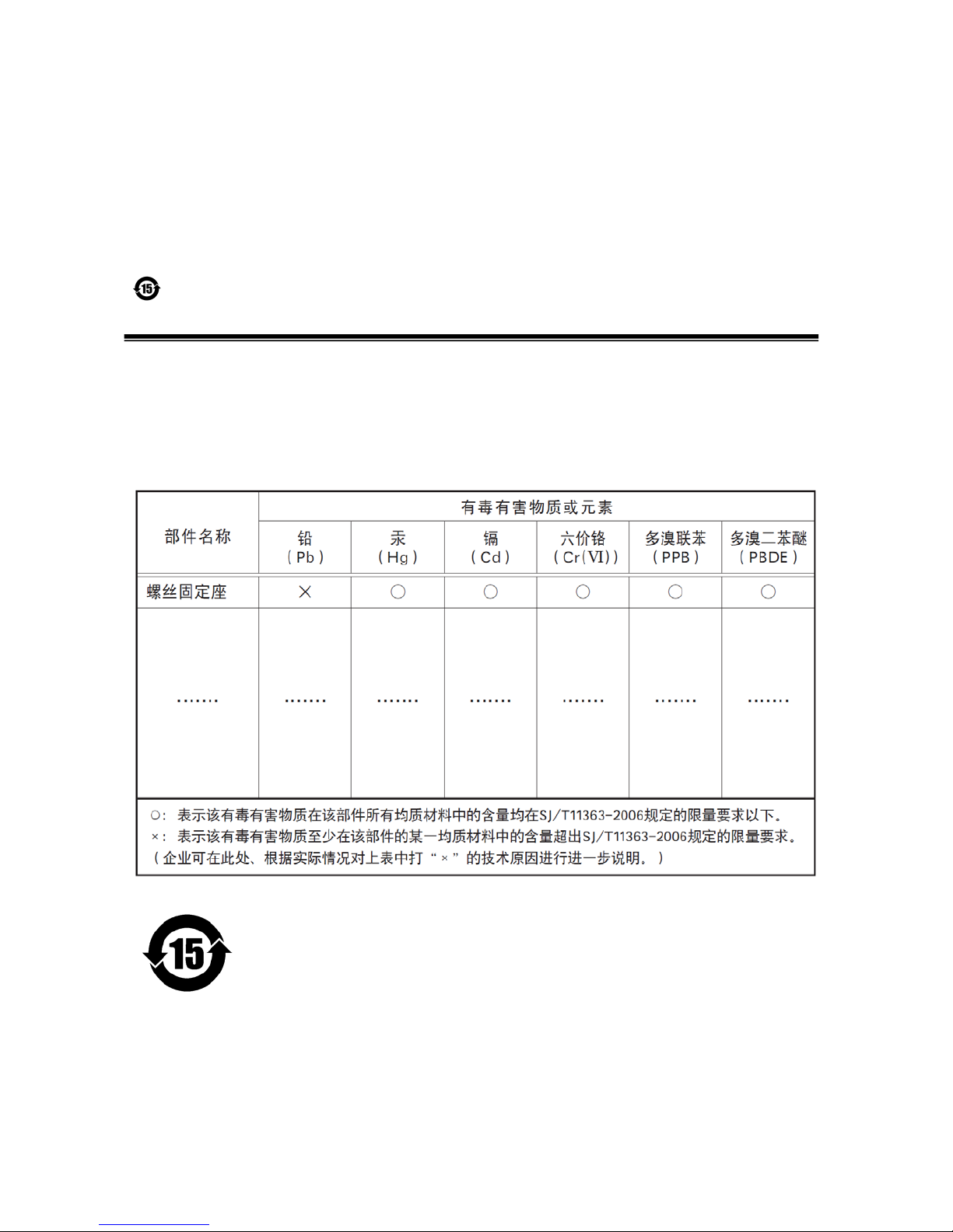
SP-20000M-PMCL
Supplement
The following statement is related to the regulation on “ Measures for the Administration
of the control of Pollution by Electronic Information Products “ , known as “ China RoHS “.
The table shows contained Hazardous Substances in this camera.
mark shows that the environment-friendly use period of contained Hazardous
Substances is 15 years.
嶷勣廣吭並㍻
嗤蕎嗤墾麗嵎賜圷殆兆各式根楚燕
功象嶄鯖繁酎慌才忽佚連恢匍何〆窮徨佚連恢瞳麟半陣崙砿尖一隈〇云恢瞳ゞ 嗤蕎嗤
墾麗嵎賜圷殆兆各式根楚燕 〃泌和
桟隠聞喘豚㍉
窮徨佚連恢瞳嶄根嗤議嗤蕎嗤墾麗嵎賜圷殆壓屎械聞喘議訳周和音氏窟伏翌
亶賜融延、窮徨佚連恢瞳喘薩聞喘乎窮徨佚連恢瞳音氏斤桟廠夛撹冢嶷麟半
賜斤児繁附、夏恢夛撹冢嶷鱒墾議豚㍉。
方忖仝15々葎豚㍉15定。
Page 4
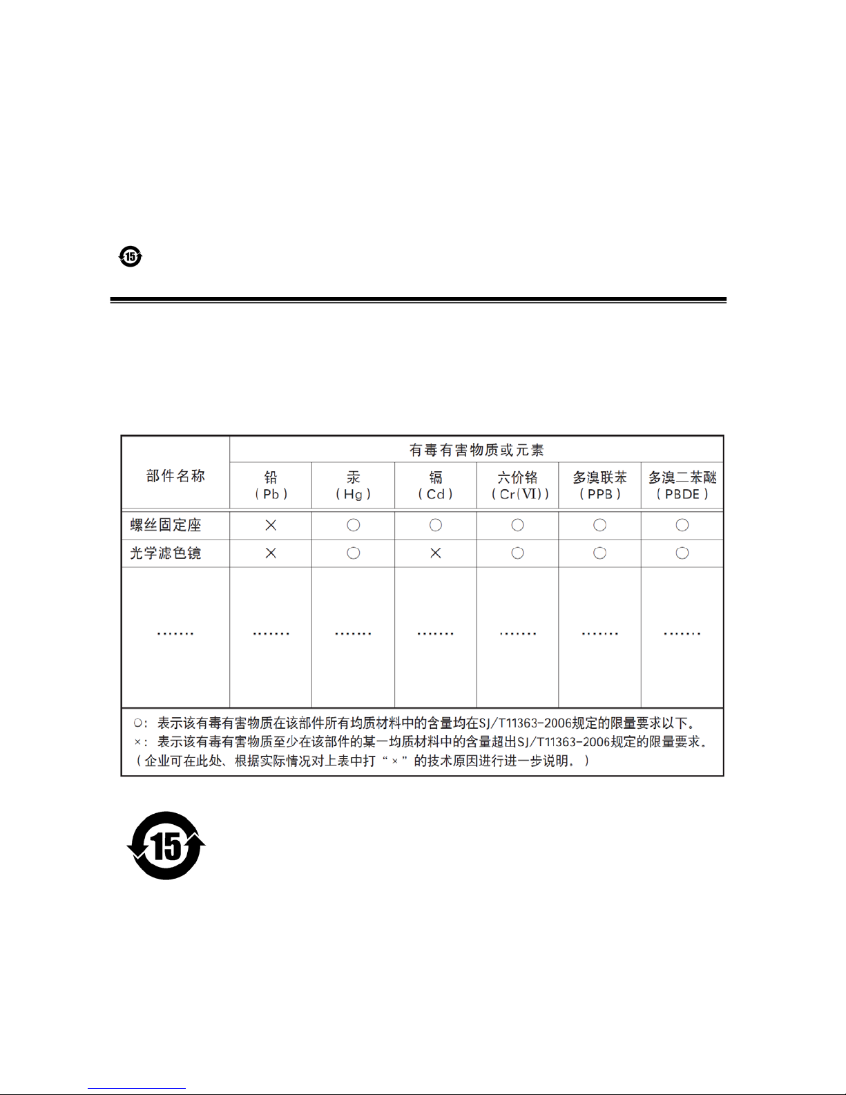
SP-20000C-PMCL
Supplement
The following statement is related to the regulation on “ Measures for the Administration
of the control of Pollution by Electronic Information Products “ , known as “ China RoHS “.
The table shows contained Hazardous Substances in this camera.
mark shows that the environment-friendly use period of contained Hazardous
Substances is 15 years.
嶷勣廣吭並㍻
嗤蕎嗤墾麗嵎賜圷殆兆各式根楚燕
功象嶄鯖繁酎慌才忽佚連恢匍何〆窮徨佚連恢瞳麟半陣崙砿尖一隈〇云恢瞳ゞ 嗤蕎嗤
墾麗嵎賜圷殆兆各式根楚燕 〃泌和
桟隠聞喘豚㍉
窮徨佚連恢瞳嶄根嗤議嗤蕎嗤墾麗嵎賜圷殆壓屎械聞喘議訳周和音氏窟伏翌
亶賜融延、窮徨佚連恢瞳喘薩聞喘乎窮徨佚連恢瞳音氏斤桟廠夛撹冢嶷麟半
賜斤児繁附、夏恢夛撹冢嶷鱒墾議豚㍉。
方忖仝15々葎豚㍉15定。
Page 5

SP-20000M-PMCL / SP-20000C-PMCL
- 3 -
- Contents -
Before using this camera ..................................................................... - 6 -
1. General .................................................................................... - 7 -
2. Camera composition .................................................................... - 7 -
3. Main features .............................................................................. - 8 -
4. Locations and functions ................................................................. - 9 -
4.1 Locations and functions ..................................................................................... - 9 -
4.2 Rear Panel .................................................................................................. - 10 -
5. Input and output .......................................................................... - 11 -
5.1 Connectors and pin assignment ........................................................................ - 11 -
5.1.1 12-Pin connector ..................................................................................... - 11 -
5.1.1.1 Figure ............................................................................................. - 11 -
5.1.1.2 Pin Assignment .................................................................................. - 11 -
5.1.2 Camera Link Connector ............................................................................. - 11 -
5.1.2.1 Figure ............................................................................................. - 11 -
5.1.2.2 Pin assignment .................................................................................. - 12 -
5.1.3 AUX connector HIROSE 10-Pin connector .................................................... - 12 -
5.2 Camera Link interface ................................................................................... - 13 -
5.2.1 Camera Link Interface .............................................................................. - 13 -
5.2.2 Camera Link Pixel clock ............................................................................ - 14 -
5.3 Digital IN/OUT Inteface .................................................................................. - 15 -
5.3.1 Line Selector ......................................................................................... - 15 -
5.3.2 Line Source ........................................................................................... - 15 -
5.3.3 Line Mode ............................................................................................. - 15 -
5.3.4 Line Inverter .......................................................................................... - 15 -
5.3.5 Line Status ............................................................................................ - 15 -
5.3.6 Line Format ........................................................................................... - 16 -
5.3.7 GPIO .................................................................................................... - 16 -
5.3.7.1 Basic block diagram ............................................................................ - 16 -
5.3.7.2 Input and output matrix table ............................................................... - 17 -
5.4 Pulse Generator ........................................................................................... - 18 -
5.4.1 Clock Pre-scaler ...................................................................................... - 18 -
5.4.2 Pulse Generator Selector ........................................................................... - 18 -
5.4.3 Pulse Generator Length ............................................................................ - 19 -
5.4.4 Pulse Generator Start Point........................................................................ - 19 -
5.4.5 Pulse Generator End Point ......................................................................... - 19 -
5.4.6 Pulse Generator Repeat Count .................................................................... - 19 -
5.4.7 Pulse Generator Clear Activation ................................................................. - 19 -
5.4.8 Pulse Generator Clear Sync Mode ................................................................. - 19 -
5.4.9 Pulse Generator Clear Source ..................................................................... - 21 -
5.4.10 Pulse Generator Inverter ......................................................................... - 22 -
5.4.11 Pulse Generator setting parameters ............................................................ - 22 -
6. Sensor layout, output format and timing ........................................ - 23 -
6.1 Sensor layout .............................................................................................. - 23 -
6.1.1 Monochrome sensor ................................................................................. - 23 -
6.1.2 Bayer sensor .......................................................................................... - 23 -
6.2 Camera output format ................................................................................... - 24 -
6.2.1 1X2-1Y ................................................................................................. - 24 -
6.2.2 1X4–1Y ................................................................................................. - 25 -
6.2.3 1X8–1Y ................................................................................................. - 25 -
6.3 Output timing .............................................................................................. - 26 -
6.3.1 Horizontal timing .................................................................................... - 26 -
6.3.2 Vertical timing ....................................................................................... - 30 -
Page 6

SP-20000M-PMCL / SP-20000C-PMCL
- 4 -
6.3.3 ROI (Region Of Interest) ............................................................................ - 33 -
6.3.4 Mirroring function ................................................................................... - 36 -
6.3.5 Multi ROI function ................................................................................... - 37 -
6.3.5.1 Multi ROI setting parameters ................................................................. - 37 -
6.4 Digital output bit allocation ............................................................................ - 39 -
7. Operating modes ...................................................................... - 40 -
7.1. Acquisition control (change the frame rate) ........................................................ - 40 -
7.1.1 Acquisition control .................................................................................. - 40 -
7.1.2 Interval calculation of frame rate(In Continuous Trigger mode) ........................ - 41 -
7.2. Exposure control ......................................................................................... - 43 -
7.2.1 Exposure Mode ....................................................................................... - 43 -
7.2.2 ExposureTime ........................................................................................ - 44 -
7.2.3 Behavior if Trigger Overlap is set to Readout .................................................. - 44 -
7.2.4 ExposureAuto ......................................................................................... - 49 -
7.3. Trigger Mode .............................................................................................. - 49 -
7.3.1 Trigger Selector ...................................................................................... - 49 -
7.3.2 Trigger Mode ......................................................................................... - 49 -
7.3.3 TriggerSource ........................................................................................ - 50 -
7.3.4 TriggerActivation .................................................................................... - 50 -
7.3.5 Trigger overlap ....................................................................................... - 50 -
7.4. Normal continuous operation (Timed Exposure Mode/Trigger Mode OFF) ..................... - 51 -
7.5. Timed (EPS) mode ....................................................................................... - 51 -
7.5.1 If Overlap setting is” OFF” ......................................................................... - 52 -
7.5.2 If Overlap setting is “Readout” ................................................................... - 53 -
7.5.3 Calculation formula for the minimum trigger interval if Trigger Overlap is OFF ........ - 54 -
7.5.4 Calculation formula for the minimum trigger interval if Trigger Overlap is Readout ... - 55 -
7.5.5 GPIO TTL output timing if Trigger Overlap is OFF ............................................. - 56 -
7.5.6 GPIO TTL output timing if Trigger Overlap is Readout ........................................ - 59 -
7.6 Trigger width mode....................................................................................... - 61 -
7.6.1 If Overlap setting is “OFF” ......................................................................... - 62 -
7.6.2 If Overlap setting is “Readout” ................................................................... - 63 -
7.6.3 Minimum trigger interval calculation formula (Trigger Overlap = OFF) .................... - 64 -
7.6.4 Minimum trigger interval calculation formula (Trigger Overlap = Readout) .............. - 65 -
7.7 PIV (Particle Image Velocimetry) ...................................................................... - 66 -
7.8 Sequential Timed Exposure mode...................................................................... - 71 -
7.8.1 Sequence ROI setting parameters ................................................................ - 72 -
7.9. Operation and function matrix ........................................................................ - 74 -
8. Other functions ........................................................................ - 75 -
8.1 Black level control ........................................................................................ - 75 -
8.1.1 Black Level Selector................................................................................. - 75 -
8.1.2 Black Level ............................................................................................ - 75 -
8.1.3 Auto black control ................................................................................... - 75 -
8.2 Gain control ................................................................................................ - 76 -
8.2.1 Gain Selector ......................................................................................... - 76 -
8.2.2 Gain .................................................................................................... - 76 -
8.2.3 Gain Auto ............................................................................................. - 76 -
8.2.4 Balance White Auto ................................................................................. - 77 -
8.3. LUT ......................................................................................................... - 77 -
8.3.1 LUT Mode ............................................................................................. - 77 -
8.3.2 LUT Index ............................................................................................. - 77 -
8.3.3 LUT Value ............................................................................................. - 77 -
8.4 Gamma...................................................................................................... - 78 -
8.5 Shading Correction ....................................................................................... - 78 -
8.6 Blemish compensation ................................................................................... - 79 -
8.7 ALC .......................................................................................................... - 80 -
8.8 HDR function (SP-20000M-PMCL only) ................................................................. - 81 -
Page 7

SP-20000M-PMCL / SP-20000C-PMCL
- 5 -
9. Camera Settings......................................................................... - 83 -
9.1 Camera Control Tool ..................................................................................... - 83 -
9.2 Camera Default Settings ................................................................................. - 83 -
10. External appearance and dimensions .......................................... - 84 -
11. Specifications ........................................................................ - 85 -
11.1. Camera spectral response ............................................................................ - 85 -
11.2. Specification table ..................................................................................... - 86 -
Appendix 1 Short ASCII Command Communication Protocol ................ - 88 -
1 Communication setting ................................................................. - 88 -
2 Protocol(Short ASCII Command) ............................................... - 88 -
2.1 Transmit the setting command to camera ........................................................... - 88 -
2.2 Transmit the request command to camera .......................................................... - 88 -
2.3 Switching baud rate between PC and camera ....................................................... - 88 -
2.4 Command list (Short ASCII command) ................................................................. - 89 -
2.4.1 GenCP Bootstrap Register .......................................................................... - 89 -
2.4.2 Tecnology Specific Bootstrap Register ........................................................... - 89 -
2.4.3 Device Control ....................................................................................... - 89 -
2.4.4 Image Format Control............................................................................... - 90 -
2.4.5 Acquistion Control ................................................................................... - 90 -
2.4.6 Digital I/O Control ................................................................................... - 91 -
2.4.7 Analog Control ....................................................................................... - 94 -
2.4.8 LUT Control ........................................................................................... - 95 -
2.4.9 Transport Layer Control ............................................................................ - 95 -
2.4.10 User Set Control .................................................................................... - 96 -
2.4.11 JAI Custom .......................................................................................... - 96 -
Appendix 2 .................................................................................. - 112 -
1. Precautions .................................................................................................. - 112 -
2. Typical Sensor Characteristics ............................................................................ - 113 -
3. Caution when mounting a lens on the camera ........................................................ - 113 -
4. Caution when mounting the camera .................................................................... - 113 -
5. Exportation .................................................................................................. - 114 -
6. References ................................................................................................... - 114 -
Manual change history .................................................................... - 115 -
User's Record ............................................................................... - 116 -
Page 8

SP-20000M-PMCL / SP-20000C-PMCL
- 6 -
Before using this camera
EMVA 1288
With regard to signal-to-noise ratio in this manual, specifications measured by EMVA 1288 are used
together with specifications by a traditional measurement method.
EMVA 1288 is a more complete measurement that considers multiple noise sources, including random
noise, pattern noise, and shading. Additionally, EMVA 1288 incorporates temporal variances in pixel
output by capturing 100 frames of data and computing the RMS variations over the captured frames.
Because of the comprehensive nature of the noise analysis and the additional consideration for RMS
variances over time, EMVA 1288 SNR measurements are inherently lower than the traditional SNR
measurements given by manufacturers. However, the comprehensive nature combined with rigid test
parameters, means that all manufacturers’ are measuring their products equally and EMVA 1288 tested
parameters can be compared among different manufacturers’ products.
In order to learn more about EMVA 1288, please visit http://www.emva.org
Frame grabber board
The SP-20000M-PMCL and SP-20000C-PMCL comply with “Power over Camera Link” which enables power
to be supplied to the camera through the Camera Link cable(s). Because the power requirements of the
camera exceed the amount of power which can be provided over a single PoCL connection, power must
be supplied via both Camera Link cables in order to utilize the PoCL capabilities. If you plan to use this
function, please be sure that the frame grabber board you are using also complies with this specification.
Alternatively, the camera can be powered via a separate power supply connected to the 12-pin Hirose
connector.
The SP-20000M-PMCL and SP-20000C-PMCL employ output formats which comply with the GenICam
Ⓡ
standard. They are 1X8-1Y (8-Tap output), 1X4–1Y (4-Tap output) and 1X2–1Y (2-Tap output). 1X8–1Y,
1X4-1Y and 1X2–1Y are available for 8-bit and 10-bit. Please check if the frame grabber used in the
system complies with the mentioned formats.
Computer used for SP-20000 series
In order to get proper performance from this camera, it is necessary to use a PC equipped with a PCIe
2.0 slot with a size and capacity of 16 lanes or higher (x16 or x32).
Camera control tool
The SP-20000M-PMCL and SP-20000C-PMCL are designed to use the JAI SDK and Control Tool software to
control camera functions. All controllable functions are stored in the camera’s XML file. The JAI SDK can
be downloaded from www.jai.com .
A camera control tool for using the Short ASCII command protocol is not available on the JAI website.
Please contact your local JAI representative if this is required.
Page 9

SP-20000M-PMCL / SP-20000C-PMCL
- 7 -
1. General
The SP-20000M-PMCL and SP-20000C-PMCL are among the first new “Spark Series” cameras to be
introduced. They provide both high resolution and a high frame rate with excellent image quality for
machine vision applications. The SP-20000M-PMCL is a monochrome progressive scan CMOS camera and
the SP-20000C-PMCL is the equivalent Bayer mosaic progressive scan CMOS camera. Both are equipped
with CMOS sensors offering a 35 mm full size image format, a resolution of 20 million pixels, and a 4:3
aspect ratio. They provide 30 frames per second for 1X8–1Y output format continuous scanning with 5120
x 3480 full pixel resolution for both monochrome and raw Bayer output.
8-bit or 10-bit output can be selected for both monochrome and raw Bayer formats. The new cameras
feature a Mini Camera Link interface which is capable of supporting a “Power over Camera Link”
capability. A full pixel readout or partial scan readout mode can be selected depending on applications.
The readout format is available from 8-tap, 4-tap or 2-tap output.
The SP-20000M-PMCL and SP-20000C-PMCL have various comprehensive functions needed for automated
optical inspection applications, such as solid state device inspection or material surface inspection. They
incorporate video processing functions such as a look-up table, flat field shading compensation and
blemish compensation in addition to fundamental functions such as trigger, exposure setting and video
level control. They also provide a new HDR (High Dynamic Range) function.
The latest version of this manual can be downloaded from: www.jai.com
The latest version of the JAI SDK for the SP-20000M-PMCL and SP-20000C-PMCL can be downloaded from:
www.jai.com
For camera revision history, please contact your local JAI distributor.
2. Camera composition
The standard camera composition is as follows.
Camera body 1
Sensor protection cap 1
Dear Customer (sheet) 1
The following optional accessories are available.
Tripod base
MP-42
Power supply unit
PD-12 series
Page 10

SP-20000M-PMCL / SP-20000C-PMCL
- 8 -
3. Main features
New Spark Series, 35mm full size, CMOS 20-megapixel progressive scan camera with global
shutter
Utilizes Mini Camera Link interface in Medium or Full configurations
Aspect ratio 4:3, 5120(H) x 3480(V) - 20 million effective pixels
6.4 μm square pixels
S/N 53dB for monochrome and 51dB for color
8-bit or 10-bit output for monochrome and Bayer
30 frames/second with full resolution in continuous operation for 8-tap output,
15 frames/second for 4-tap output and 7.5 fps for 2-tap output for both monochrome and Bayer
Vertical and horizontal binning on monochrome model
Supports ROI (Region Of Interest) modes for faster frame rate
0dB to +24dB gain control for both SP-20000M-PMCL and SP-20000C-PMCL
304 μs (1/3290) to 8 seconds exposure control in 1 μs step
Auto exposure control
Timed and trigger width exposure control
PIV and sequential trigger modes for specific applications
ALC control with combined function of AGC and auto exposure
HDR (High Dynamic Range) function is available (SP-20000M-PMCL only)
Various pre-processing circuits are provided
Programmable LUT
Gamma correction from 0.45 to 1.0
Shading correction
Bayer white balance with manual or one-push auto (SP-20000C-PMCL only)
Blemish compensation
Auto iris lens video output with H-sync
New Hirose 10P connector for TTL IN and OUT and LVDS IN interface
F-mount for lens mount
Accepts power over Mini Camera Link or via 12-pin connector
Setup by Windows XP/Vista/7/8 via serial communication
Page 11
SP-20000M-PMCL / SP-20000C-PMCL
- 9 -
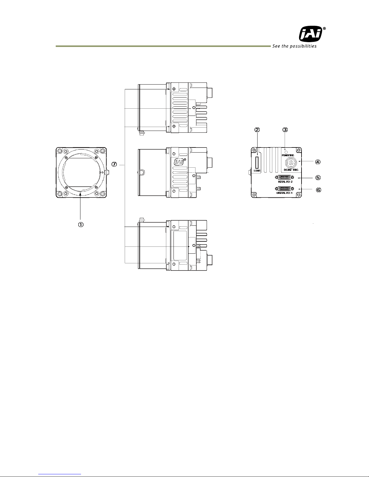
4. Locations and functions
4.1 Locations and functions
Lens mount F-mount (Note *1)
10-pin connector AUX connector for TTL IN/OUT and LVDS IN
LED Indication for power and Trigger input
12-pin connector DC+12V and Trigger input
Camera Link Connector 2 Digital video output (Medium and Full configuration) (Note *2)
Camera Link Connector 1 Digital video output (Base, Medium and Full config.) (Note *2)
Mounting holes M3 depth 5 mm for fixing the camera to the tripod base or
direct installation (Note *3)
*1) Note: Rear protrusion on F-mount lens must be less than 40.0 mm.
*2) Note: When a Camera Link cable is connected to the camera, please do not excessively tighten
screws by using a driver. The Camera Link receptacle on the camera might be damaged.
For security, the strength to tighten screws is less than 0.147 Newton meter (Nm).
Tightening by hand is sufficient in order to achieve this.
*3) Note: The part number for the tripod adapter plate (with 1/4"-20 thread) is MP-42 (option).
Fig. 1 Locations
Page 12

SP-20000M-PMCL / SP-20000C-PMCL
- 10 -
4.2 Rear Panel
The rear panel mounted LED provides the following information:
Amber: Power connected – initiating
This light goes OFF after initiating.
Steady green: Camera is operating in Continuous mode
Flashing green: The camera is receiving external triggering
Note: The interval of flashing does not correspond with external
trigger duration.
Fig. 2 Rear panel
Page 13
SP-20000M-PMCL / SP-20000C-PMCL
- 11 -
5. Input and output
5.1 Connectors and pin assignment
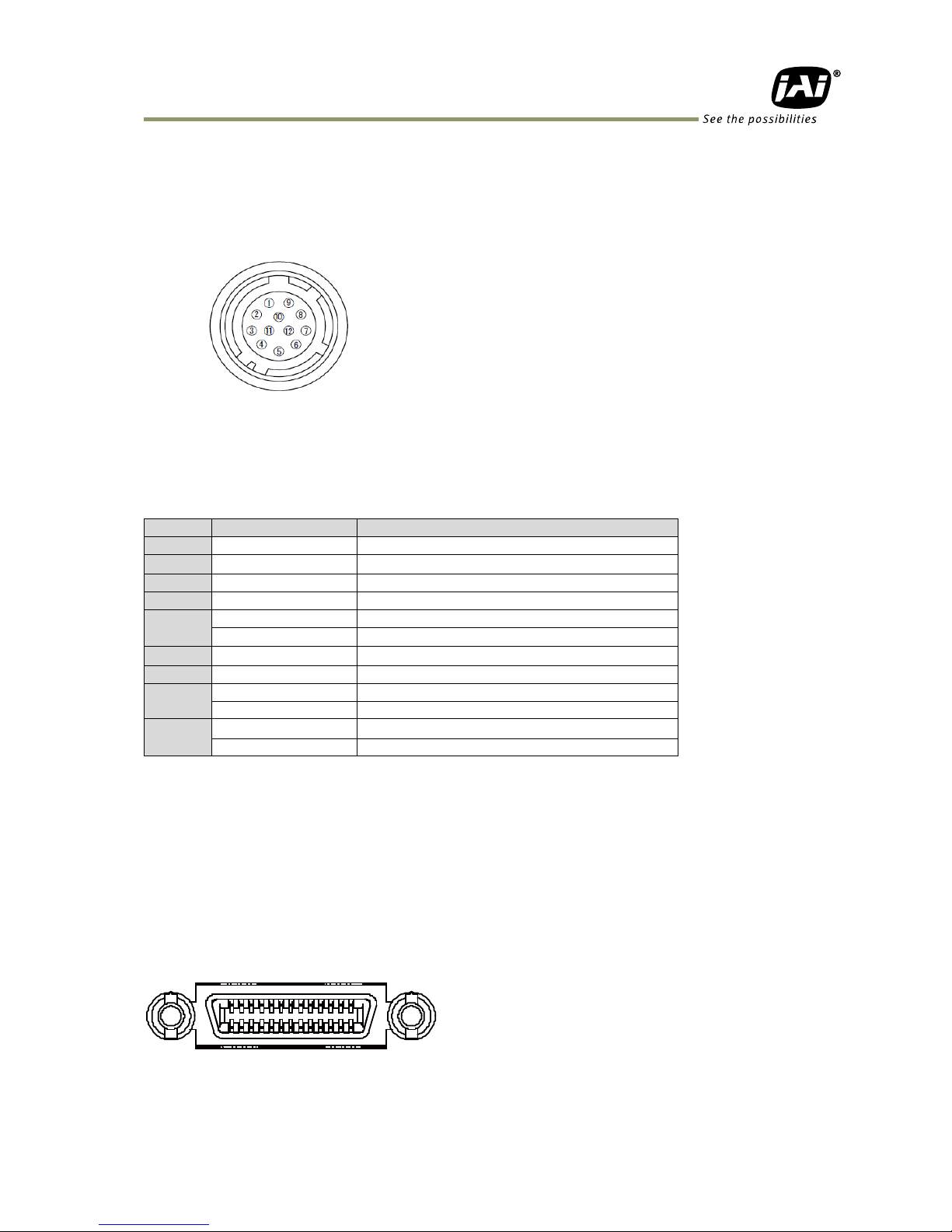
5.1.1 12-Pin connector
5.1.1.1 Figure
Type: HR-10A-10R-12PB(72) Hirose male or equivalent
Use the part number HR10A-10P-12S or equivalent for the cable
side.
5.1.1.2 Pin Assignment
Table 1 12-pin configuration
Note 1) Factory default setting is Exposure Active and negative
Although Exposure Active is positive in the inside of the camea, it is output from TTL Out 1
after being inverted to negative.
Note 2) Factory default setting is trigger input.
Note 3) See page 6 for notes about power options for these cameras
5.1.2 Camera Link Connector
5.1.2.1 Figure
Type: 26-pin Mini Camera Link connector (Honda HDR-EC26FYTG2-SL+)
See page 6 for notes about Power over Camera Link (PoCL) options for this camera.
Fig.4 Camera Link connector
1
14
13
26
Pin no.
Signal
Remarks 1 GND
2
DC input
+12V ~ +24V (note 3)
3
GND
4
Video Iris
For lens auto iris
5
NC
6
NC
7
NC
8
NC
9
TTL Out 1
Line1 (note 1)
10
TTL In 1
Line4 (note 2)
11
DC input
+12V ~ +24V (note 3)
12
GND
Fig.3 Hirose 12-pin connector
Page 14
SP-20000M-PMCL / SP-20000C-PMCL
- 12 -
5.1.2.2 Pin assignment
Table-2 Camera link pin configuration – connector 1
Pin No
In/Out
Name
Note
1,26 Power
Power
2(-),15(+)
O
X_OUT0
Data output
3(-),16(+)
O
X_OUT1
4(-),17(+)
O
X_OUT2
5(-),18(+)
O
X_Clk
Clock for CL
6(-),19(+)
O
X_OUT3
Data output
7(+),20(-)
I
SerTC (RxD)
LVDS serial control
8(-),21(+)
O
SerTFG (TxD)
9(-),22(+)
I
CC1 (Trigger)
Trigger input
10(+),23(-)
CC1 (Reserved)
11,24 N.C
12,25 N.C
13,14
Shield
Power Return
Camera Link connector 2
Pin No
In/Out
Name
Note
1,26 Power
Power
2(-),15(+)
O
Y_OUT0
Data output
3(-),16(+)
O
Y_OUT1
4(-),17(+)
O
Y_OUT2
5(-),18(+)
O
Y_Clk
Clock for CL
6(-),19(+)
O
Y_OUT3
Data output
7(+),20(-)
I
N.C
8(-),21(+)
O
Z_OUT0
Data output
9(-),22(+)
I
Z_OUT1
10(+),23(-)
Z_OUT2
11,24 Z_Clk
Clock for CL
12,25
Z_OUT3
Data output
13,14
Shield
Power Return
5.1.3 AUX connector HIROSE 10-Pin connector
Type: HIROSE 10-Pin Connector 3260-10S3(55)
Fig. 5 Hirose 10p connector
Table-3 Pin configuration for Hirose 10P AUX connector
No
I/O
Name
Note 1 O
TTL OUT2
Line8 2 O
TTL OUT3
Line9 3 I
TTL IN2
Line10 4
NC
5
GND
6 I
LVDS IN1+
Line11
7
I
LVDS IN1-
8
NC
9
GND
10
GND
1
8
Page 15
SP-20000M-PMCL / SP-20000C-PMCL
- 13 -
5.2 Camera Link interface
5.2.1 Camera Link Interface
Table-4 Camera Link interface
Base Medium Full 80bit
2Tap / 10bit 4Tap / 10bit 8 Tap / 8b it 8 Tap / 10 bit
1X2 - 1Y 1X4 - 1Y 1x8 - 1Y 1X8 - 1Y
Port A0 TxIN 0 Tap 1 D0 Tap 1 D0 Tap 1 D0 T ap 1 D2
Port A1 TxIN 1 Tap 1 D1 Tap 1 D1 Tap 1 D1 T ap 1 D3
Port A2 TxIN 2 Tap 1 D2 Tap 1 D2 Tap 1 D2 T ap 1 D4
Port A3 TxIN 3 Tap 1 D3 Tap 1 D3 Tap 1 D3 T ap 1 D5
Port A4 TxIN 4 Tap 1 D4 Tap 1 D4 Tap 1 D4 T ap 1 D6
Port A5 TxIN 6 Tap 1 D5 Tap 1 D5 Tap 1 D5 T ap 1 D7
Port A6 Tx IN 27 Tap 1 D6 Tap 1 D6 Tap 1 D6 T ap 1 D8
Port A7 TxIN 5 Tap 1 D7 Tap 1 D7 Tap 1 D7 T ap 1 D9
Port B0 TxIN 7 Tap 1 D8 Tap 1 D8 Tap 2 D0 T ap 2 D2
Port B1 TxIN 8 Tap 1 D9 Tap 1 D9 Tap 2 D1 T ap 2 D3
Port B2 TxIN 9 ― ― Tap 2 D2 Tap 2 D4
Port B3 TxIN 12 ― ― Tap 2 D3 Tap 2 D5
Port B4 TxIN 13 Tap 2 D8 Tap 2 D8 T ap 2 D4 T ap 2 D6
Port B5 TxIN 14 Tap 2 D9 Tap 2 D9 T ap 2 D5 T ap 2 D7
Port B6 TxIN 10 ― ― Tap 2 D6 Tap 2 D8
Port B7 TxIN 11 ― ― Tap 2 D7 Tap 2 D9
Port C0 TxIN 15 Tap 2 D0 Tap 2 D0 Tap 3 D0 T ap 3 D2
Port C1 TxIN 18 Tap 2 D1 Tap 2 D1 Tap 3 D1 T ap 3 D3
Port C2 TxIN 19 Tap 2 D2 Tap 2 D2 Tap 3 D2 T ap 3 D4
Port C3 TxIN 20 Tap 2 D3 Tap 2 D3 Tap 3 D3 T ap 3 D5
Port C4 TxIN 21 Tap 2 D4 Tap 2 D4 Tap 3 D4 T ap 3 D6
Port C5 TxIN 22 Tap 2 D5 Tap 2 D5 Tap 3 D5 T ap 3 D7
Port C6 TxIN 16 Tap 2 D6 Tap 2 D6 Tap 3 D6 T ap 3 D8
Port C7 TxIN 17 Tap 2 D7 Tap 2 D7 Tap 3 D7 T ap 3 D9
- TxIN 24 LVAL LVAL LVAL LVAL
- TxIN 25 FVAL FVAL FVAL FVAL
(Port I0) TxIN 26 DVAL DVAL DVAL Tap 1 D0
(Port I1) TxIN 23 Exposure Active Exposure Active Exposure Active Tap 1 D1
SP-20000M/C-PMCL
Camera Link Configuration
Camera Link port/bit
GenICam Tap Geometry
D
i
g
i
t
a
l
I
/
O
-
1
Port
Base Medium Full 80bit
2Tap / 10bit 4Tap / 10bit 8 Tap / 8b it 8 Tap / 10 bit
1X2 - 1Y 1X4 - 1Y 1x8 - 1Y 1X 8 - 1Y
Port D0 TxIN 0 ― Tap 4 D0 Tap 4 D0 T ap 4 D2
Port D1 TxIN 1 ― Tap 4 D1 Tap 4 D1 T ap 4 D3
Port D2 TxIN 2 ― Tap 4 D2 Tap 4 D2 T ap 4 D4
Port D3 TxIN 3 ― Tap 4 D3 Tap 4 D3 T ap 4 D5
Port D4 TxIN 4 ― Tap 4 D4 Tap 4 D4 T ap 4 D6
Port D5 TxIN 6 ― Tap 4 D5 Tap 4 D5 T ap 4 D7
Port D6 TxI N 27 ― Tap 4 D6 Tap 4 D6 Tap 4 D8
Port D7 TxIN 5 ― Tap 4 D7 Tap 4 D7 T ap 4 D9
Port E0 TxIN 7 ― Tap 3 D0 Tap 5 D0 T ap 5 D2
Port E1 TxIN 8 ― Tap 3 D1 Tap 5 D1 T ap 5 D3
Port E2 TxIN 9 ― Tap 3 D2 Tap 5 D2 T ap 5 D4
Port E3 TxI N 12 ― Tap 3 D3 T ap 5 D3 T ap 5 D5
Port E4 TxI N 13 ― Tap 3 D4 T ap 5 D4 T ap 5 D6
Port E5 TxI N 14 ― Tap 3 D5 T ap 5 D5 T ap 5 D7
Port E6 TxI N 10 ― Tap 3 D6 T ap 5 D6 T ap 5 D8
Port E7 TxI N 11 ― Tap 3 D7 T ap 5 D7 T ap 5 D9
Port F0 TxIN 15 ― T ap 3 D8 T ap6 D0 T ap 6 D2
Port F1 TxIN 18 ― T ap 3 D9 T ap6 D1 T ap 6 D3
Port F2 TxIN 19 ― ― Tap6 D2 Tap 6 D4
Port F3 TxIN 20 ― ― Tap6 D3 Tap 6 D5
Port F4 TxIN 21 ― T ap 4 D8 T ap6 D4 T ap 6 D6
Port F5 TxIN 22 ― T ap 4 D9 T ap6 D5 T ap 6 D7
Port F6 TxIN 16 ― ― Tap6 D6 Tap 6 D8
Port F7 TxIN 17 ― ― Tap6 D7 Tap 6 D9
- TxIN 24 ― LVAL L VAL LVAL
(Port I2) TxIN 25 ― FVAL FVAL Tap 2 D0
(Port I3) TxIN 26 ― DVAL DVAL T ap 2 D1
(Port I4) TxIN 23 ― Ex posure Active Exposure Active Tap 3 D0
D
i
g
i
t
a
l
I
/
O
-
2
(
1
/
2
)
SP-20000M/C-PMCL
Port
Camera Link Configuration
Camera Link port/bit
GenICam Tap Geometry
Page 16
SP-20000M-PMCL / SP-20000C-PMCL
- 14 -
Note
1. In this table, all Tap Geometry items are not described. For instance, 1X2–1Y and 1X4–1Y show only
10-bit. In case of 8-bit, upper 2 bits (D8 and D9) are not used.
2. Please check whether the frame grabber complies with those formats if you use 80-bit (8Tap/10-bit)
camera configuration.
3. If you use 80-bit (8Tap/10-bit) camera configuration, DVAL and Exposure Active (JAI custom) are
not output through the Camera Link interface. FVAL is only output via Digital I/O-1 connector.
5.2.2 Camera Link Pixel clock
The SP-20000M-PMCL and SP-20000C-PMCL use the Camera Link pixel clock of 80 MHz as the
default setting. It can be changed.
Table – 5 Camera Link pixel clock
Camera Link
Pixel Clock
Tap
Geometry
Camera Link
Configuration
Note
80 MHz
1X8-1Y
80-bit, Full
Defaut setting
1X4-1Y
Medium
1X2-1Y
Base
60 MHz
1X8-1Y
80-bit, Full
1X4-1Y
Medium
1X2-1Y
Base
[Note]
If the Camera Link pixel clock is changed, the output is immediately changed but it may
take a few seconds for the output signal to be stable.
Base Medium Full 80bit
2Tap / 10bit 4Tap / 10 bit 8 Tap / 8b it 8 Tap / 10bit
1X2 - 1Y 1X 4 - 1Y 1x8 - 1Y 1X 8 - 1Y
Port G0 TxIN 0 ― ― Tap 7 D0 Tap 7 D2
Port G1 TxIN 1 ― ― Tap 7 D1 Tap 7 D3
Port G2 TxIN 2 ― ― Tap 7 D2 Tap 7 D4
Port G3 TxIN 3 ― ― Tap 7 D3 Tap 7 D5
Port G4 TxIN 4 ― ― Tap 7 D4 Tap 7 D6
Port G5 TxIN 6 ― ― Tap 7 D5 Tap 7 D7
Port G6 TxIN 27 ― ― Tap 7 D6 Tap 7 D8
Port G7 TxIN 5 ― ― Tap 7 D7 Tap 7 D9
Port H0 TxIN 7 ― ― Tap 8 D0 Tap 8 D2
Port H1 TxIN 8 ― ― Tap 8 D1 Tap 8 D3
Port H2 TxIN 9 ― ― Tap 8 D2 Tap 8 D4
Port H3 TxIN 12 ― ― T ap 8 D3 T ap 8 D5
Port H4 TxIN 13 ― ― T ap 8 D4 T ap 8 D6
Port H5 TxIN 14 ― ― T ap 8 D5 T ap 8 D7
Port H6 TxIN 10 ― ― T ap 8 D6 T ap 8 D8
Port H7 TxIN 11 ― ― T ap 8 D7 T ap 8 D9
(Port I5) TxIN 15 ― ― ― Tap 3 D1
(Port I6) TxIN 18 ― ― ― Tap 4 D0
(Port I7) TxIN 19 ― ― ― Tap 4 D1
(Port K0) TxIN 20 ― ― ― Tap 5 D0
(Port K1) TxIN 21 ― ― ― Tap 5 D1
(Port K2) TxIN 22 ― ― ― Tap 6 D0
(Port K3) TxIN 16 ― ― ― Tap 6 D1
(Port K4) TxIN 17 ― ― ― Tap 7 D0
- TxIN 24 ― ― LVAL LVAL
(Port K5) TxIN 25 ― ― FVAL Tap 7 D1
(Port K6) TxIN 26 ― ― DVAL Tap 8 D0
(Port K7) TxIN 23 ― ― Exposure Active Tap 8 D1
D
i
g
i
t
a
l
I
/
O
-
2
(
2
/
2
)
SP-20000M/C-PMCL
Port
Camera Link Configuration
Camera Link port/bit
GenICam Tap Geometry
Page 17
SP-20000M-PMCL / SP-20000C-PMCL
- 15 -
5.3 Digital IN/OUT Inteface
In the SP-20000M-PMCL and SP-20000C-PMCL, the software control tool can assign the necessary
signals used in the system to digital inputs and outputs.
5.3.1 Line Selector
In the Line Selector, the following input and output signals can be assigned.
Table-6 Line selector
5.3.2 Line Source
Line source signal can be selected from the following table to connect it to the line item which
is selected in the Line Selector.
Table-7 Line Source
5.3.3 Line Mode
Indicates the status of the item selected in Line Selector. (INPUT or OUTPUT)
5.3.4 Line Inverter
Inverts the signal polarity for the item selected in Line Selector.
(False=Positive, True=Negative)
5.3.5 Line Status
Indicates the status of the selected signal (input or output) (True=High,
False=Low)
Line Selector item
Description
Line 1 TTL 1 Out
TTL output from # 9 pin of DC In/Trigger 12-Pin on the rear
Line 8 TTL 2 Out
TTL output from #1pin “AUX” HIROSE 10-Pin on the rear
Line 9 TTL 3 Out
TTL output from #2pin “AUX” HIROSE 10-Pin on the rear
NAND 0 In 1
First input at NAND first gate in GPIO
NAND 0 In 2
Second input at NAND first gate in GPIO
NAND 1 In 1
First input at NAND second gate in GPIO
NAND 1 in 2
Second input at NAND second gate in GPIO
Line Source item
Description
Low
Connect Low Level signal to line item selected in Line Selector, Default setting
High
Connect High Level signal to line item selected in Line Selector
Frame Trigger Wait
Connect Frame Trigger Wait signal to line item selected in Line Selector
Frame Active
Connect Frame Active signal to line item selected in Line Selector
Exposure Active
Connect Exposure Active signal to line item selected in Line Selector
FVAL
Connect FVAL signal to line item selected in Line Selector
LVAL
Connect LVAL signal to line item selected in Line Selector
PulseGenerator0 Out
Connect Pulse Generator 0 signal to line item selected in Line Selector
PulseGenerator1 Out
Connect Pulse Generator 1 signal to line item selected in Line Selector
PulseGenerator2 Out
Connect Pulse Generator 2 signal to line item selected in Line Selector
PulseGenerator3 Out
Connect Pulse Generator 3 signal to line item selected in Line Selector
TTL 1 In
Connect TTL 1 IN signal to line item selected in Line Selector
CL CC1 In
Connect CL CC1 IN signal to line item selected in Line Selector
Nand0 Out
Connect NAND 0 signal to line item selected in Line Selector
Nand1 Out
Connect NAND 1 signal to line item selected in Line Selector
Line 10 TTL 2 In
Connect TTL 2 IN signal to Line 10
Line 11 LVDS 1 In
Connect LVDS 1 IN signal to Line 11
Note: As for LVAL, some line items can not be connected. Refer to “5.4.6.2 GPIO matrix table”
Page 18
SP-20000M-PMCL / SP-20000C-PMCL
- 16 -
5.3.6 Line Format
Controls the format of the line item selected in Line Selector.
(No Connect, TTL, LVDS, Opt Coupled)
Note: The SP-20000-PMCL does not have “Opto Coupled” in and out interface.
5.3.7 GPIO
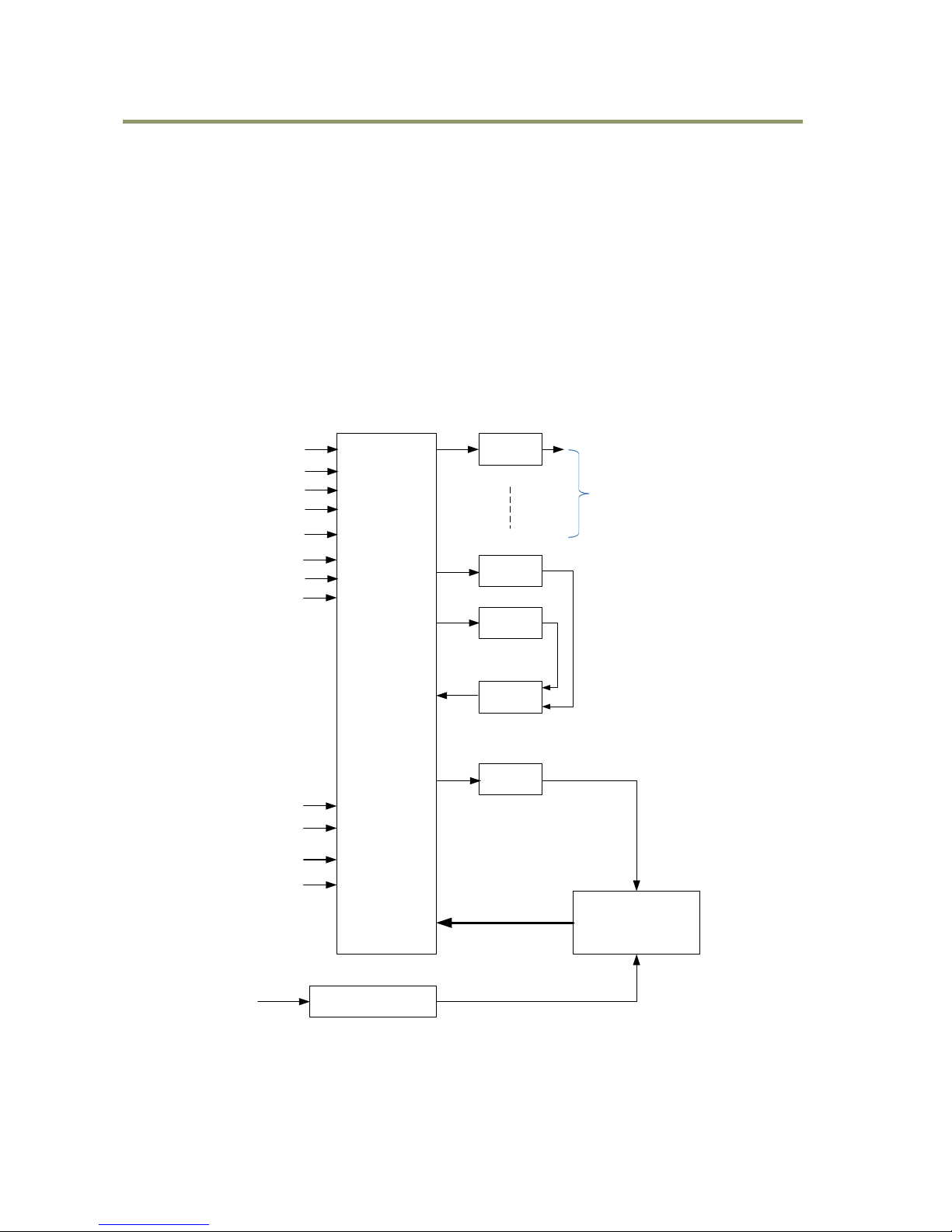
GPIO is a general interface for input and output and controls the I/O for trigger signals and
other valid signals and pulse generators. By using this interface you can control an external light
source, make a delay function for an external trigger signal, or make a precise exposure setting
together with a PWC trigger.
5.3.7.1 Basic block diagram
The basic block diagram is as follows.
Soft Trigger
LVAL IN
FVAL IN
Exposure Active
Acquisition Trigger Wait
Acquisition Active
Frame Trigger Wait
Frame Active
Line 4 (TTL IN 1)
Line 7 (CL CC1)
Line 10 (TTL IN2)
Line 11 (LVDS IN)
Pixel Clock
Cross Point
Switch
12 bit Counter
INV
INV
INV N
NAND
INV
Non INV
Pulse Generator
20 bit counter x 4
CLR
Sel Bit (5,0) Sel Bit (7)
Sel Bit (7)
Pulse Generator 0
Pulse Generator 1
Pulse Generator 2
Pulse Generator 3
Trigger 2 (Frame Start)
Line 1 (TTL OUT 1)
Line 8 (TL OUT 2)
Line 9 (TTL OUT 3)
Sel Bit (7)
Clock IN
Clear IN
Gate 1
Gate 2
Fig.6 GPIO interface
Page 19
SP-20000M-PMCL / SP-20000C-PMCL
- 17 -
5.3.7.2 Input and output matrix table
The relation between input and output is as follows.
Table-8 GPIO matrix table
Selector (Cross
point switch output)
Source signal
(Cross point switch input)
Low
High
Soft Trigger
Exposure Active
Frame Trigger Wait
Frame Active
FVAL
LVAL
Pulse Generator 0
Pulse Generator 1
Pulse Generator 2
Pulse Generator 3
Line 4 - TTL In1
Line 7 - CL CC1 in
NAND 0 Out
NAND 1 Out 1
Line 10 - TTL 2 In
Line 11 - LVDS 1 In
Trigger Source
Pulse Generator
Clear Source
Line Source
Line 9 - TTL 3 Out
NAND 1 In 1
NAND 1 In 2
NAND 2 In 1
NAND 2 In 2
Pulse Generator 0
Pulse Generator 1
Pulse Generator 2
Pulse Generator 3
Line Selector
Pulse Generator
Selector
Trigger Source
(Frame Start )
Line 1 - 12P TTL Out
Line 8 - TTL 2 Out
Trigger Selector
Page 20
SP-20000M-PMCL / SP-20000C-PMCL
- 18 -
5.4 Pulse Generator
The SP-20000-PMCL series has a frequency divider using the sensor clock as the basic clock and
four pulse generators. In each Pulse Generator, various Clear settings are connected to GPIO.
The following shows Pulse Generator default settings.
Table - 9 Pulse Generator default settings
5.4.1 Clock Pre-scaler
Clock pre-scaler (Divide Value) can set the dividing value of the frequency divider (12-bit
length) and the sensor clock is used for this. Four built-in pulse generators work by the
same clock. In the SP-20000-PMCL, the sensor pixel clock is 39.16 MHz.
5.4.2 Pulse Generator Selector
This is where you select one of the 4 pulse generators in order to set or modify its
parameters.
Table - 10 Pulse Generator setting
Display Name
Value
Clock Pre-scaler
1
Pulse Generator
Selector
Pulse Generator
Length
Start
Point
End
Point
Repeat
Count
Clear
Source
Clear
Inverter
Clear
Activation
Clear
Sync
Mode
-
Pulse Generator 0
1 0 1 0 Off
True
Off
Async Mode
-
Pulse Generator 1
1 0 1 0 Off
True
Off
Async Mode
-
Pulse Generator 2
1 0 1 0 Off
True
Off
Async Mode
-
Pulse Generator 3
1 0 1 0 Off
True
Off
Async Mode
Note:]
When Pulse Generator Repeat Count is set to “0”, the camera is operating in free-running mode.
However, based on the above default settings, Length=1, Start Point=0 and End Point=1, Pulse Generator stops at High
output. Therefore, if Start Point =0 and End Point=1 are configured, Length should be “2” as the minimum active
width.
Trigger Selector
item
Description
Pulse Generator 0
If Pulse Generator 0 is selected, Length, Start Point, End Point, Repeat Count, Clear Source, Clear
Inverter, Clear Activation and Clear Sync Mode of Pulse Generator 0 are displayed under the
selector.
Pulse Generator 1
If Pulse Generator 1 is selected, Length, Start Point, End Point, Repeat Count, Clear Source, Clear
Inverter, Clear Activation and Clear Sync Mode of Pulse Generator 1 are displayed under the
selector.
Pulse Generator 2
If Pulse Generator 2 is selected, Length, Start Point, End Point, Repeat Count, Clear Source, Clear
Inverter, Clear Activation and Clear Sync Mode of Pulse Generator 2 are displayed under the
selector.
Pulse Generator 3
If Pulse Generator 3 is selected, Length, Start Point, End Point, Repeat Count, Clear Source, Clear
Inverter, Clear Activation and Clear Sync Mode of Pulse Generator 3 are displayed under the
selector.
Page 21
SP-20000M-PMCL / SP-20000C-PMCL
- 19 -
Fig.7 Pulse Generator pulse construction
5.4.3 Pulse Generator Length
Set the counter up value (number of clocks, refer to Table 12) for the selected pulse
generator. If Repeat Count value is “0”, and if Pulse Generator Clear signal is not input,
the
pulse generator generates the pulse repeatedly until reaching this counter up value.
5.4.4 Pulse Generator Start Point
Set the active output start count value for the selected pulse generator.
However, please note that a maximum 1 clock jitter for the clock which is divided in the clock
pre-scaler can occur.
5.4.5 Pulse Generator End Point
Set the active output ending count value for the selected pulse generator.
5.4.6 Pulse Generator Repeat Count
Set the repeating number of the pulse for the selected pulse generator. After Trigger Clear
signal is input, the pulse generator starts the count set in Repeat Count. Accordingly, an
active pulse which has a start point and end point can be output repeatedly.
However, if Repeat Count is set to “0”, it works as free-running counter.
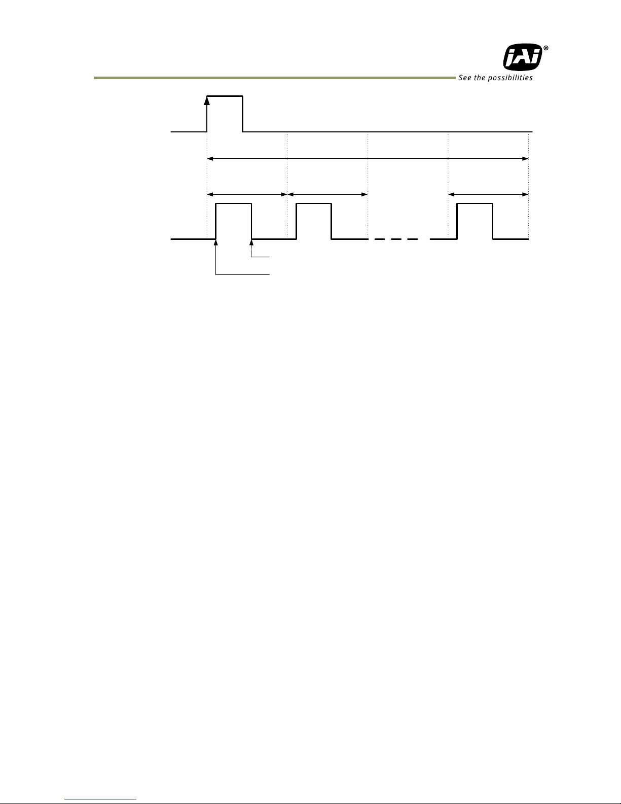
5.4.7 Pulse Generator Clear Activation
Set the clear conditions of clear count pulse for the selected pulse generator.
5.4.8 Pulse Generator Clear Sync Mode
Set the count clear method for the selected pulse generator.
In case of Async Mode, if the clear signal is input during the length setting value, the counter
will stop counting according to the clear signal input.
In case of Sync Mode, if the clear signal is input during the length setting value, the counter
will continue to count until the end of the length setting value and then clear the count.
Both modes clear the repeat count when the counter is cleared.
Pulse generator
length
Pulse generator Start point
Pulse generator End point
Pulse generator repeat count = N
(Pulse generator length x N)
Pulse generator
Clear source IN
(Clear activation
= Rising edge
Clear SYNC mode
= Async)
Pulse generator
Output
Pulse generator
length
Pulse generator
length
000
Page 22
SP-20000M-PMCL / SP-20000C-PMCL
- 20 -
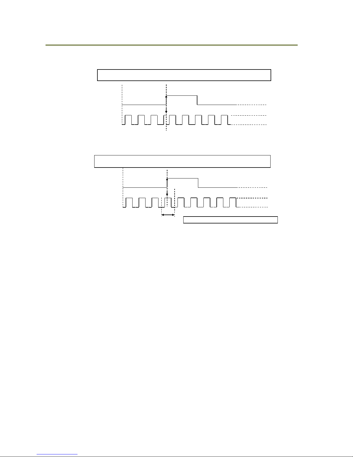
Fig.8 Counter clear in Async mode
Fig.9 Counter clear in Sync mode
0
Clear
↓
Pulse
Generator
Output
Pulse
Generator
Clear Source In
(Example 1) Clear Activation = Rising Edge, Clear Sync Mode = Async Mode,
Clear Inverter = False
(Example 2) Clear Activation = Rising Edge, Clear Sync Mode = Sync Mode,
Clear Inverter = False
Pulse
Generator
Output
Pulse
Generator
Clear Source In
0
Pulse
Generator
Length
0
Clear
↓
Note: Repeat Count is also reset.
Page 23
SP-20000M-PMCL / SP-20000C-PMCL
- 21 -
5.4.9 Pulse Generator Clear Source
The following clear source can be selected as the pulse generator clear signal.
Tabel - 11 Pulse generator clear source
Pulse Generator
Clear Source
item
Description
Low
Connect Low level signal to Clear Source for the selected pulse generator.
Default setting
High
Connect High level signal to Clear Source for the selected pulse generator.
Frame Trigger Wait
Connect Frame Trigger Wait signal to Clear Source for the selected pulse
generator.
Frame Active
Connect Frame Active signal to Clear Source for the selected pulse
generator.
Exposure Active
Connect Exposure Active signal to Clear Source for the selected pulse
generator.
FVAL
Connect FVAL signal to Clear Source for the selected pulse generator.
LVAL
Connect LVAL signal to Clear Source for the selected pulse generator.
PulseGenerator0
Out
Connect Pulse Generator 0 output to Clear Source for the selected pulse
generator.
PulseGenerator1
Out
Connect Pulse Generator 1 output to Clear Source for the selected pulse
generator.
PulseGenerator2
Out
Connect Pulse Generator 2 output to Clear Source for the selected pulse
generator.
PulseGenerator3
Out
Connect Pulse Generator 3 output to Clear Source for the selected pulse
generator.
TTL 1 In
Connect TTL 1 IN signal to Clear Source for the selected pulse generator.
CL CC1 In
Connect CL CC1 IN signal to Clear Source for the selected pulse generator.
Nand0 Out
Connect NAND 0 output signal to Clear Source for the selected pulse
generator.
Nand1 Out
Connect NAND 1 output signal to Clear Source for the selected pulse
generator.
Line 10 TTL 2 In
Connect TTL 2 IN signal to LINE 10.
Line 11 LVDS 1 In
Connect LVDS 1 IN signal to Line 11
Note:
The pulse generator output cannot be used as the clear input to the same pulse generator. Refer
to “5.4.6.2.GPIO matrix table”.
Page 24
SP-20000M-PMCL / SP-20000C-PMCL
- 22 -
5.4.10 Pulse Generator Inverter
Clear Source Signal can be have polarity inverted.
5.4.11 Pulse Generator setting parameters
Table - 12 Pulse Generator setting parameters
Display Name
Value
Clock Pre-scaler
1 to 4096
Pulse Generator Clock (MHzMHz)
[Pixel Clock:39.16 MHz]÷[Clock Pre-scaler]
Pulse Generator Selector
- Pulse Generator 0
- Pulse Generator 1
- Pulse Generator 2
- Pulse Generator 3
- Pulse Generator Length
1 to 1048575
- Pulse Generator Length (ms)
([Clock Source]÷[Clock Pre-scaler])-1 x [Pulse Generator Length]
- Pulse Generator Frequency (Hz)
[ Pulse Generator Length (ms)]-1
- Pulse Generator Start Point
0 to 1048574
- Pulse Generator Start Point (ms)
([Clock Source]÷[Clock Pre-scaler])-1 x [Pulse Generator Start Point]
- Pulse Generator End Point
1 to 1048575
- Pulse Generator End Point (ms)
([Clock Source]÷[Clock Pre-scaler])-1 x [Pulse Generator End Point]
- Pulse Generator pulse-width (ms)
[ Pulse Generator End Point (ms)]-[ Pulse Generator Start Point (ms)]
- Pulse Generator Repeat Count
0 to 255
- Pulse Generator Clear Activation
Clear Mode for the Pulse Generators
- Off
- High Level
- Low level
- Rising Edge
- Falling Edge
- Pulse Generator Clear Sync Mode
- Async mode
- Sync mode
- Pulse Generator Clear Source
- Low
- High
- Frame Trigger Wait
- Frame Active
- Exposure Active
- Fval
- Lval
- PulseGenerator0
- PulseGenerator1
- PulseGenerator2
- PulseGenerator3
- TTL_In1
- CL_CC1_In
- Nand0 Out
- Nand1 Out
- Line 10 - TTL 2 In
- Line 11 - LVDS 1 In
- Pulse Generator Inverter(Polarity)
Pulse Generator Clear Inverter
- False
- True
Note:
1. If Pulse Generator Repeat Count is set to “0”, the pulse generator works in free-running mode.
2. The output of the same pulse generator cannot be connected to Clear input.
3. If the Camera Link pixel clock is changed, the pixel clock of the pulse generator remains 39.16 MHz.
Page 25
SP-20000M-PMCL / SP-20000C-PMCL
- 23 -
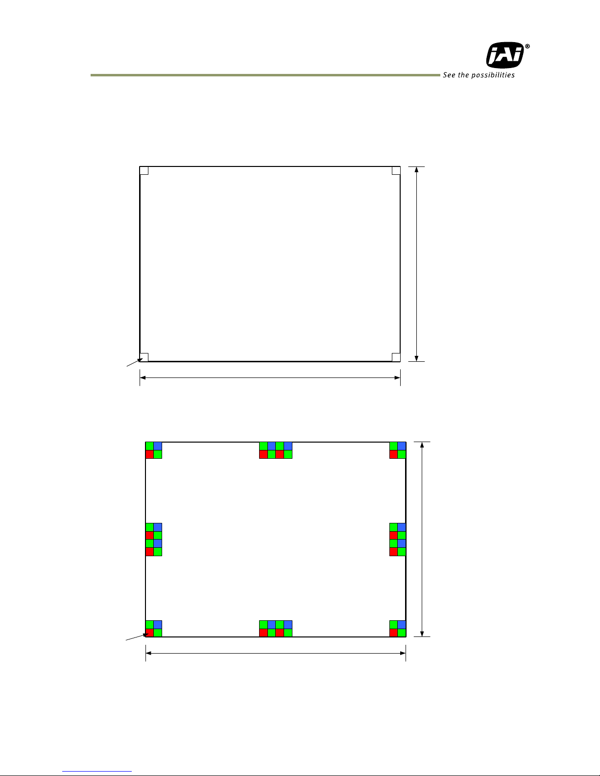
6. Sensor layout, output format and timing
6.1 Sensor layout
The CMOS sensors used in the SP-20000-PMCL have the following pixel layout.
6.1.1 Monochrome sensor
Fig. 10 Monochrome sensor layout
6.1.2 Bayer sensor
Fig. 11 Color sensor layout
5120 Pixels
3840 Pixels
F
Pixel (0,0)
5120 Pixels
3840 Pixels
F
Pixel (0,0)
Page 26
SP-20000M-PMCL / SP-20000C-PMCL
- 24 -
6.2 Camera output format
Table - 13 Output format
Camera output format
Pixel format
Refer to drawing
1X2–1Y
8-bit, 10-bit
6.2.1
1X4–1Y
8-bit, 10-bit
6.2.2
1X8–1Y
8-bit, 10-bit
6.2.3
Note: The camera output description is based on GenICam SFNC Ver.1.5.1.
6.2.1 1X2-1Y
1X2–1Y is a 2-tap readout system specified in GenICam Tap Geometry and it outputs as
follows.
Width = 5120 Pixel 2560 Pixel x 2 Taps
Height = 3840 Pixel
X5120
Y1
X5120
Y3840
X4
Y1
X4
Y3840
X3
Y1
X3
Y3840
X2
Y1
X2
Y3840
X5
Y1
X5
Y3840
X6
Y1
X6
Y3840
X7
Y1
X7
Y3840
X8
Y1
X8
Y3840
X5113
Y1
X5113
Y3840
X5114
Y1
X5114
Y3840
X5115
Y1
X5115
Y3840
X5116
Y1
X5116
Y3840
X5117
Y1
X5117
Y3840
X5118
Y1
X5118
Y3840
X5119
Y1
X5119
Y3840
X5120
Y1
X5120
Y2
X5120
Y3839
X5120
Y3840
X1
Y1
X1
Y2
X1
Y3839
X1
Y3840
Tap 1
Tap 2
Pixel(0,0)
Step Y = 1
Step X = 2
Fig. 12 1X2-1Y camera output format
Page 27
SP-20000M-PMCL / SP-20000C-PMCL
- 25 -
6.2.2 1X4–1Y
1X4–1Y is a 4-tap readout system specified in GenICam Tap Geometry and it outputs as follows.
Fig. 13 1X4–1Y output system
6.2.3 1X8–1Y
1X 8–1Y is an 8-tap readout system and outputs as follows.
Fig. 14. 1X8–1Y output sysytem
Width = 5120 Pixel 1280 Pixel x 4 Taps
Height = 3840 Pixel
X5120
Y1
X5120
Y3840
X4
Y1
X4
Y3840
X3
Y1
X3
Y3840
X2
Y1
X2
Y3840
X5
Y1
X5
Y3840
X6
Y1
X6
Y3840
X7
Y1
X7
Y3840
X8
Y1
X8
Y3840
X5113
Y1
X5113
Y3840
X5114
Y1
X5114
Y3840
X5115
Y1
X5115
Y3840
X5116
Y1
X5116
Y3840
X5117
Y1
X5117
Y3840
X5118
Y1
X5118
Y3840
X5119
Y1
X5119
Y3840
X5120
Y1
X5120
Y2
X5120
Y3839
X5120
Y3840
X1
Y1
X1
Y2
X1
Y3839
X1
Y3840
Tap 1
Tap 2
Pixel(0,0)
Step Y = 1
Step X = 4
Tap 3
Tap 4
Width = 5120 Pixel 640 Pixel x 8 Taps
Height = 3840 Pixel
X5120
Y1
X5120
Y3840
X4
Y1
X4
Y3840
X3
Y1
X3
Y3840
X2
Y1
X2
Y3840
X5
Y1
X5
Y3840
X6
Y1
X6
Y3840
X7
Y1
X7
Y3840
X8
Y1
X8
Y3840
X5113
Y1
X5113
Y3840
X5114
Y1
X5114
Y3840
X5115
Y1
X5115
Y3840
X5116
Y1
X5116
Y3840
X5117
Y1
X5117
Y3840
X5118
Y1
X5118
Y3840
X5119
Y1
X5119
Y3840
X5120
Y1
X5120
Y2
X5120
Y3839
X5120
Y3840
X1
Y1
X1
Y2
X1
Y3839
X1
Y3840
Tap 1
Tap 2
Pixel(0,0)
Step Y = 1
Step X = 8
Tap 3
Tap 4
Tap 5
Tap 6
Tap 7
Tap 8
Page 28
SP-20000M-PMCL / SP-20000C-PMCL
- 26 -
6.3 Output timing
6.3.1 Horizontal timing
This timing is for the continuous trigger. The horizontal frequency is changed by the setting of
Tap Geometry. The SP-20000M-PMCL (monochrome) supports horizontal and vertical binning.
However, the horizontal frequency does not change when horizontal binning is effective, and
therefore, the frame rate is not increased.
FVAL Active
(a) LVAL Active (b)
(c) H-Offset
FVAL
LVAL
DVAL
DATA
DVAL Active
(d)
Exposure
Active
(Camera Link
“Spare” bit)
Fig. 15 Horizontal timing per 1 tap
Page 29
SP-20000M-PMCL / SP-20000C-PMCL
- 27 -
Table – 14 Continuous trigger horizontal timing
Camera Settings
(a)
(b)
(c)
(d)
Tap Geometry Camera
Link
Pixel
Clock
ROI
Binning
LVAL
Active
LVAL
Non-Active
H-Offset
Exposure
Active Start
to
LVAL
Active Start
Step
(Typ.)
Width
Offset
X
Height
Offset Y Horiz
ontal
Verti
cal
[Unit:
Clock]
[Unit:
Clock]
[Unit:
Clock]
[Unit:
Camera Link Clock]
1X8
-1Y
80M
Hz
5120 0 3840
0
1
(Off) 1 (Off)
640
14~15 0 53
8
5120 0 1920
0
1
(Off) 2 (On)
640
669~670
0
53
or
707 8 2560 0 3840
0
2
(On) 1 (Off)
320
334~335 0 53
8
2560 0 1920
0
2
(On) 2 (On)
320
989~990
0
53
or
707
8
60M
Hz
5120 0 3840
0
1
(Off) 1 (Off)
640
19~20 0 53
10
5120 0 1920
0
1
(Off) 2 (On)
640
678~679
0
53
or
713
10
2560 0 3840
0
2
(On) 1 (Off)
320
339~340 0 53
10
2560 0 1920
0
2
(On) 2 (On)
320
998~999
0
53
or
713
10
1X4
-1Y
80M
Hz
5120 0 3840
0
1
(Off) 1 (Off)
1280
29~30 0 650
16
5120 0 1920
0
1
(Off) 2 (On)
1280
1339~1340
0
650
or
1959
16
2560 0 3840
0
2
(On) 1 (Off)
640
669~670 0 650
16
2560 0 1920
0
2
(On) 2 (On)
640
1979~1980
0
650
or
1959
16
60M
Hz
5120 0 3840
0
1
(Off) 1 (Off)
1280
38~39
0
653
22
5120 0 1920
0
1
(Off) 2 (On)
1280
1357~1358
0
653
or
1972
22
2560 0 3840
0
2
(On) 1 (Off)
640
678~679 0 653
22
2560 0 1920
0
2
(On) 2 (On)
640
1997~1998
0
653
or
1972
22
1X2
-1Y
80M
Hz
5120 0 3840
0
1
(Off) 1 (Off)
2560
58~59 0 1290
33
5120 0 1920
0
1
(Off) 2 (On)
2560
2677~2678
0
1290
or
3909
33
2560 0 3840
0
2
(On) 1 (Off)
1280
1339~1340 0 1290
33
2560 0 1920
0
2
(On) 2 (On)
1280
3957~3958
0
1290
or
3909
33
60M
Hz
5120 0 3840
0
1
(Off) 1 (Off)
2560
77~78 0 1301
44
5120 0 1920
0
1
(Off) 2 (On)
2560
2714~2715
0
1301
or
3939
44
2560 0 3840
0
2
(On) 1 (Off)
1280
1357~1358 0 1301
44
2560 0 1920
0
2
(On) 2 (On)
1280
3994~3995
0
1301
or
3939
44
Note:
1. In 1X8-1Y, 10-bit setting (80-bit Configuration), DVAL output port is used for data output and therefore, DVAL is not output through
Camera Link interface.
2. In the SP-20000-PMCL, the horizontal frequency is not doubled even if horizontal binning is ON.
3. In the SP-20000-PMCL, the horizontal frequency is 1/2 if vertical binning is ON. And if vertical binning is ON, the invalid data is output
in non-active range (H-offset range) of DVAL during LVAL being active.
4. H-Offset: Duration between LVAL Active Start and DVAL Active Start.
5. The phase of Exposure Active is described based on using the output at Camera Link Spare bit as the reference.
6. If the next exposure is done while the image of V-Binnig On is read out, the exposure control is increased or decreased by 0.5 line unit.
7. “d” ExposureActive Start to LVALActiveStart may have 1 clock difference due to the jitter in LVALNonActive period.
Page 30
SP-20000M-PMCL / SP-20000C-PMCL
- 28 -
Table – 15 Continuous trigger horizontal frequency (1X8–1Y, 1X4–1Y)
In the following table, values in “Actual operation” are real operating values. However, “1 Line Total
Clock” values in “Calculation” are used to calculate the frame rate and other. This is because jitter
occurs in “LVAL Non Active” period.
Camera Settings
Tap Geometry Camera Link Pixel
ROI
Binning
1Line
Total
Clock
Horizontal
Frequency
Horizontal
Period
Width
Offset
X
Height
Offset
Y
Horiz
ontal
Verti
cal
[Unit: Clock]
[Unit: kHz]
[Unit: us]
1X8
-1Y
80
MHz
5120 0 3840
0
1
(Off) 1 (Off)
Actual
operation
654 or 655
122.324 or
122.137
8.175 or
8.188
Calculation
654.63
122.206
8.183
5120 0 1920
0
1
(Off) 2 (On)
Actual
operation
1309 or 1310
61.115 or
61.068
16.363 or
16.375
Calculation
1309.27
61.103
16.366
2560 0 3840
0
2
(On) 1 (Off)
Actual
operation
654 or 655
122.324 or
122.137
8.175 or
8.188
Calculation
654.63
122.206
8.183
2560 0 1920
0
2
(On) 2 (On)
Actual
operation
1309 or 1310
61.115 or
61.068
16.363 or
16.375
Calculation
1309.27
61.103
16.366
60
MHz
5120 0 3840
0
1
(Off) 1 (Off)
Actual
operation
659 or 660
91.047 or
90.909
10.983 or
11.000
Calculation
659.31
91.004
10.989
5120 0 1920
0
1
(Off) 2 (On)
Actual
operation
1318 or 1319
45.523 or
45.489
21.967 or
21.983
Calculation
1318.61
45.502
21.977
2560 0 3840
0
2
(On) 1 (Off)
Actual
operation
659 or 660
91.047 or
90.909
10.983 or
11.000
Calculation
659.31
91.004
10.989
2560 0 1920
0
2
(On) 2 (On)
Actual
operation
1318 or 1319
45.523 or
45.489
21.967 or
21.983
Calculation
1318.61
45.502
21.977
1X4
-1Y
80
MHz
5120 0 3840
0
1
(Off) 1 (Off)
Actual
operation
1309 or 1310
61.115 or
61.069
16.363 or
16.375
Calculation
1309.27
61.103
16.366
5120 0 1920
0
1
(Off) 2 (On)
Actual
operation
2618 or 2619
30.558 or
30.546
32.725 or
32.738
Calculation
2618.53
30.551
32.732
2560 0 3840
0
2
(On) 1 (Off)
Actual
operation
1309 or 1310
61.115 or
61.069
16.363 or
16.375
Calculation
1309.27
61.103
16.366
2560 0 1920
0
2
(On) 2 (On)
Actual
operation
2618 or 2619
30.558 or
30.546
32.725 or
32.738
Calculation
2618.53
30.551
32.732
60
MHz
5120 0 3840
0
1
(Off) 1 (Off)
Actual
operation
1318 or 1319
45.524 or
45.489
21.967 or
21.983
Calculation
1318.61
45.502
21.977
5120 0 1920
0
1
(Off) 2 (On)
Actual
operation
2637 or 2638
22.753 or
22.745
43.950 or
43.967
Calculation
2637.23
2560 0 3840
0
2
(On) 1 (Off)
Actual
operation
1318 or 1319
45.524 or
45.489
21.967 or
21.983
Calculation
1318.61
45.502
21.977
2560 0 1920
0
2
(On) 2 (On)
Actual
operation
2637 or 2638
22.753 or
22.745
43.950 or
43.967
Calculation
2637.23
22.751
43.954
Page 31

SP-20000M-PMCL / SP-20000C-PMCL
- 29 -
Table – 16 Continuous trigger horizontal frequency (1X2–1Y)
In the following table, values in “Actual operation” are real operating values. However, “1 Line Total
Clock” values in “Calculation” are used to calculate the frame rate and other. This is because jitter
occurs in “LVAL Non Active” period.
Camera Settings
Tap Geometry Camera Link Pixel
ROI
Binning
1Line
Total
Clock
Horizontal
Frequency
Horizontal
Period
Width
Offset
X
Height
Offset
Y
Horiz
ontal
Verti
cal
[Unit: Clock]
[Unit: kHz]
[Unit: us]
1X2
-1Y
80
MHz
5120 0 3840
0
1
(Off) 1 (Off)
Actual
operation
2618
or
2619
30.558
or
30.546
32.725
or
32.738
Calculation
2618.54
30.551
32.732
5120 0 1920
0
1
(Off) 2 (On)
Actual
operation
5237
or
5238
15.276
or
15.273
65.463
or
65.475
Calculation
5237.09
15.276
65.464
2560 0 3840
0
2
(On) 1 (Off)
Actual
operation
2618
or
2619
30.558
or
30.546
32.725
or
32.738
Calculation
2618.54
30.551
32.732
2560 0 1920
0
2
(On) 2 (On)
Actual
operation
5237
or
5238
15.276
or
15.273
65.463
or
65.475
Calculation
5237.09
15.276
65.464
60
MHz
5120 0 3840
0
1
(Off) 1 (Off)
Actual
operation
2637
or
2638
25.349
or
22.745
39.450
or
43.967
Calculation
2637.25
22.751
43.954
5120 0 1920
0
1
(Off) 2 (On)
Actual
operation
5274
or
5275
11.377
or
11.374
87.900
or
87.917
Calculation
5274.49
11.376
87.908
2560 0 3840
0
2
(On) 1 (Off)
Actual
operation
2637
or
2638
25.349
or
22.745
39.450
or
43.967
Calculation
2637.25
22.751
43.954
2560 0 1920
0
2
(On) 2 (On)
Actual
operation
5274
or
5275
11.377
or
11.374
87.900
or
87.917
Calculation
5274.49
11.376
87.908
[Note]
“Actual operation” shows the real operating values that can be expected. However, in order to calculate the frame rate and so on, the
value of 1 Line Total Clock in the calculation is used. This is because jitter occurs in the LVAL Non Active period.
Page 32

SP-20000M-PMCL / SP-20000C-PMCL
- 30 -
6.3.2 Vertical timing
In Continuous Trigger operation, the output through the Camera Link interface is as follows.
However, if 80-bit (1X8-1Y, 10-bits) configuration is set, DVAL and Exposure Active
(JAI CUSTOM) are not output through Camera Link “Spare” bit because this port is used
for data output.
The SP-20000-PMCL can support H-Binning and V-Binning functions, but the frame rate is
not increased.
FVAL
LVAL
DVAL
DATA
Exposure
Active
(Camera Link
“Spare” bit)
Exposure time (Min)
FVAL Active (A)
(B)
(C) V-Offset 0 Line
DVAL Active (A)
(F) Exposure End to FVAL Active Start
(E) Exposure time (Max)
(D)
Fig. 16 Vertical timing
Page 33

SP-20000M-PMCL / SP-20000C-PMCL
- 31 -
Table – 17 Continuous trigger vertical timing (1/2)
Camera Settings
(A)
(B)
(C)
(D)
Tap Geometr
y
Camera Link Pixel Clock
Frame
Rate
(Typ.)
ROI
Binning
FVAL &
DVAL
Active
FVAL
Non
-Active
V -Offset
Exposure
Time
(Min)
Width
Offset
X
Height
Offset
Y
Horizontal
Vertical
[Unit: Line]
[Unit: Line]
[Unit: Line]
[Unit: us]
Time
1X8
-1Y
80
MHz
33333
5120 0 3840
0
1
(Off) 1 (Off)
3840
233.53
0
10.0
5120 0 1920
0
1
(Off) 2 (On)
1920
117.27
2560 0 3840
0
2
(On) 1 (Off)
3840
234.02
2560 0 1920
0
2
(On) 2 (On)
1920
117.51
60
MHz
44444
5120 0 3840
0
1
(Off) 1 (Off)
3840
204.65
0
10.0
5120 0 1920
0
1
(Off) 2 (On)
1920
102.82
2560 0 3840
0
2
(On) 1 (Off)
3840
205.13
2560 0 1920
0
2
(On) 2 (On)
1920
103.07
1X4
-1Y
80
MHz
66666
5120 0 3840
0
1
(Off) 1 (Off)
3840
233.53
0
10.0
5120 0 1920
0
1
(Off) 2 (On)
1920
117.27
2560 0 3840
0
2
(On) 1 (Off)
3840
234.02
2560 0 1920
0
2
(On) 2 (On)
1920
117.51
60
MHz
88888
5120 0 3840
0
1
(Off) 1 (Off)
3840
204.60
0
10.0
5120 0 1920
0
1
(Off) 2 (On)
1920
102.80
2560 0 3840
0
2
(On) 1 (Off)
3840
205.09
2560 0 1920
0
2
(On) 2 (On)
1920
103.04
1X2
-1Y
80
MHz
133333
5120 0 3840
0
1
(Off) 1 (Off)
3840
233.53
0
10.0
5120 0 1920
0
1
(Off) 2 (On)
1920
117.27
2560 0 3840
0
2
(On) 1 (Off)
3840
234.02
2560 0 1920
0
2
(On) 2 (On)
1920
117.51
60
MHz
177777
5120 0 3840
0
1
(Off) 1 (Off)
3840
204.62
0
10.0
5120 0 1920
0
1
(Off) 2 (On)
1920
102.81
2560 0 3840
0
2
(On) 1 (Off)
3840
205.11
2560 0 1920
0
2
(On) 2 (On)
1920
103.05
Page 34

SP-20000M-PMCL / SP-20000C-PMCL
- 32 -
Table – 18 Continuous trigger vertical timing (2/2)
Camera Settings (E)
(F)
Tap Geometry Camera Link Pixel Clock
Frame
Rate
(Typ.)
ROI
Binning
Frame
Rate
Exposure
Time
(Max.)
Exposure
End
to
FVAL
Active
Start
Width
Offset
X
Height
Offset
Y
Horizontal
Vertical
Time
[Unit: Hz]
[Unit: us]
[Unit: Line]
[Unit: us]
1X8-
1Y
80
MHz
33333
5120 0 3840
0
1
(Off) 1 (Off)
30.000
ROUNDDOWN(
[Frame Rate (Time)] -
(20600clk ÷ 80 ))
= 33075
39.10
319.96
5120 0 1920
0
1
(Off) 2 (On)
20.05
328.15
2560 0 3840
0
2
(On) 1 (Off)
39.10
319.96
2560 0 1920
0
2
(On) 2 (On)
20.05
328.15
60
MHz
44444
5120 0 3840
0
1
(Off) 1 (Off)
22.500
ROUNDDOWN(
[Frame Rate (Time)] -
(20600clk ÷ 60 ))
= 44100
39.10
429.68
5120 0 1920
0
1
(Off) 2 (On)
20.05
440.68
2560 0 3840
0
2
(On) 1 (Off)
39.10
429.68
2560 0 1920
0
2
(On) 2 (On)
20.05
440.68
1X4-
1Y
80
MHz
66666
5120 0 3840
0
1
(Off) 1 (Off)
15.000
ROUNDDOWN(
[Frame Rate (Time)] -
(20600clk ÷ 80 ))
= 66408
20.05
328.15
5120 0 1920
0
1
(Off) 2 (On)
10.53
344.51
2560 0 3840
0
2
(On) 1 (Off)
20.05
328.15
2560 0 1920
0
2
(On) 2 (On)
10.53
344.51
60
MHz
88888
5120 0 3840
0
1
(Off) 1 (Off)
11.250
ROUNDDOWN(
[Frame Rate (Time)] -
(20600clk ÷ 60 ))
= 88544
20.05
440.67
5120 0 1920
0
1
(Off) 2 (On)
10.53
462.63
2560 0 3840
0
2
(On) 1 (Off)
20.05
440.67
2560 0 1920
0
2
(On) 2 (On)
10.53
462.63
1X2-
1Y
80
M Hz
133333
5120 0 3840
0
1
(Off) 1 (Off)
7.500
ROUNDDOWN(
[Frame Rate (Time)] -
(41200clk ÷ 80 ))
= 132818
20.05
656.20
5120 0 1920
0
1
(Off) 2 (On)
10.52
688.93
2560 0 3840
0
2
(On) 1 (Off)
20.05
656.20
2560 0 1920
0
2
(On) 2 (On)
10.52
688.93
60
MHz
177777
5120 0 3840
0
1
(Off) 1 (Off)
5.625
ROUNDDOWN(
[Frame Rate (Time)] -
(41200clk ÷ 60 ))
= 177090
20.05
881.22
5120 0 1920
0
1
(Off) 2 (On)
10.52
925.17
2560 0 3840
0
2
(On) 1 (Off)
20.05
881.22
2560 0 1920
0
2
(On) 2 (On)
10.52
925.17
Note:
1. As the frame rate of the SP-20000-PMCL is 1 µs duration per 1 step, the above FVAL Non-Active conversion may have certain
tolerance.
2. In the SP-20000-PMCL, the horizontal frequency is not doubled even if horizontal binning is used. The frame rate is not increased.
3. In the SP-20000-PMCL, the horizontal frequency is 1/2 if vertical binning is used. Therefore, if the height is 1/2, the vertical frequency
is not doubled.
4. In the SP-20000-PMCL, the frame rate can be changed by 1 µs unit. In the above table, “B” FVAL Non-Active duration is
varied.
5. V-Offset : The duration between FVAL Active Start and 1st LVAL Active Start
Page 35

SP-20000M-PMCL / SP-20000C-PMCL
- 33 -
6.3.3 ROI (Region Of Interest)
In the SP-20000-PMCL, a subset of the image can be output by setting Width, Height, Offset-X,
and Offset-Y. If the height is decreased, the number of lines read out is decreased and as the
result, the frame rate is increased. However, in the horizontal directon, the horizontal
frequency is not changed if the width is decreased. In the SP-20000-PMCL, the minimum width
is “8” and minimum height is “2”.
]
Note: Binning is available only for
SP-20000M-PMCL.
Binning can be used in horizontal,
vertical, or both directions.
Fig. 17 Setting example ( No binning) Fig.18 Setting example (Binning)
Setting example (1)
Binning Horizontal = 1
Binning Vertical = 1
Mirroring = Off
Setting example (2)
Binning Horizontal = 2
Binning Vertical = 2
Mirroring = Off
OffsetX
OffsetY
Height
Width
2560 Width Max
1920 Height Max
Readout area
OffsetX
Width
OffsetY
Height
Width
5120 Width Max
3840 Height Max
Readout area
Page 36

SP-20000M-PMCL / SP-20000C-PMCL
- 34 -
Table - 19 ROI setting examples (1/2)
ROI
Camera Settings
ROI
Binning
Width
Max
Height
Max
Max
Offset
X
Value
Width and
Offset
X
Step
Max
Offset
Y
Value
Height
Step
Offset
Y
Step
Width Offset X Height Offset Y Horizontal Vertical
1X8
-1Y
1X4
-1Y
1X2
-1Y
Full Line
5120 0 3840
0
1
(Off) 1 (Off)
5120
3840 0 8 8 8 0 2
1
2/3 Screen
- Center
3408
856
2560
640
1
(Off) 1 (Off)
5120
3840
1712 8 8 8 1280 2 1
1/2 Screen
- Center
2560
1280
1920
960
1
(Off) 1 (Off)
5120
3840
2560 8 8 8 1920 2 1
1/4 Screen
- Center
1280
1920
960
1440
1
(Off) 1 (Off)
5120
3840
3840 8 8 8 2880 2 1
1/8 Screen
- Center
640
2240
480
1680
1
(Off) 1 (Off)
5120
3840
4480 8 8 8 3360 2 1
Full Line
2560 0 1920
0
2
(On) 2 (On)
2560
1920 0 8 8 8 0 1
1
2/3 Screen
- Center
1704
428
1280
320
2
(On) 2 (On)
2560
1920
856 8 8 8 640 1 1
1/2 Screen
- Center
1280
640
960
480
2
(On) 2 (On)
2560
1920
1280 8 8 8 960 1 1
1/4 Screen
- Center
640
960
480
720
2
(On) 2 (On)
2560
1920
1920 8 8 8 1440 1 1
1/8 Screen
- Center
320
1120
240
840
2
(On) 2 (On)
2560
1920
2240 8 8 8 1680 1 1
[Note : Setting restrictions
1. [Width Max] = 5120, [Height Max] = 3840 (H and V Binning Off) (If it is On, the value is 1/2)
2. [Max Offset X Value] = [Width Max] - [Width] :Maximum value which Offset X can be set
3. [Max Offset Y Value] = [Height Max] - [Height]:Maximum value which Offset Y can be set
4. [Width and Offset X Step]:The step number which Width and horizontal offset can be shifted
5. [Height and Offset Y Step]:The step number which Height and vertical offset can be shifted
Page 37

SP-20000M-PMCL / SP-20000C-PMCL
- 35 -
Table - 20 ROI setting examples (Frame rate)
ROI 考
Camera Settings
Frame Rate (Typ.)
ROI
Binning
Tap Geometry
Width
Offset X
Height
Offset Y
Horizontal
Vertica
l
1X8-1Y
1X4-1Y
1X2-1Y
Camera Link
Pixel Clock
Camera Link
Pixel Clock
Camera Link
Pixel Clock
80 MHz
60 MHz
80 MHz
60 MHz
80 MHz
60 MHz
Full Line
5120 0 3840
0
1
(Off) 1 (Off)
Setting
value
[Unit: us]
33333
44444
66666
88888
133333
177777
Output
[Unit: Hz]
30.000
22.500
15.000
11.250
7.500
5.625
2/3
Screen
- Center
3408
856
2560
640
1
(Off) 1 (Off)
Setting
value
[Unit: us]
22222
29629
44444
59259
88889
118518
Output
[Unit: Hz]
44.998
33.751
22.500
16.875
11.250
8.4375
1/2
Screen
- Center
2560
1280
1920
960
1
(Off) 1 (Off)
Setting
value
[Unit: us]
16667
22222
33333
44444
66667
88889
Output
[Unit: Hz]
59.998
45.000
30.000
22.500
15.000
11.250
1/4
Screen
- Center
1280
1920
960
1440
1
(Off) 1 (Off)
Setting
value
[Unit: us]
8428
11318
16856
22636
33713
45272
Output
[Unit: Hz]
118.64
88.352
59.325
44.176
29.662
22.088
1/8
Screen
- Center
640
2240
480
1680
1
(Off) 1 (Off)
Setting
value
[Unit: us]
4500
6043
9001
12087
18002
24174
Output
[Unit: Hz]
222.18
165.46
111.09
82.728
55.549
41.366
Full Line
2560 0 1920
0
2
(On) 2 (On)
Setting
value
[Unit: us]
33333
44444
66666
88888
133333
177777
Output
[Unit: Hz]
30.000
22.500
15.000
11.250
7.500
5.625
2/3
Screen
- Center
1704
428
1280
320
2
(On) 2 (On)
Setting
value
[Unit: us]
22222
29629
44444
59258
88889
118518
Output
[Unit: Hz]
44.998
33.751
22.500
16.875
11.250
8.4375
1/2
Screen
- Center
1280
640
960
480
2
(On) 2 (On)
Setting
value
[Unit: us]
16667
22222
33333
44444
66667
88889
Output
[Unit: Hz]
59.998
45.000
30.000
22.500
15.000
11.250
1/4
Screen
- Center
640
960
480
720
2
(On) 2 (On)
Setting
value
[Unit: us]
8412
11296
16824
22592
33648
45184
Output
[Unit: Hz]
118.87
88.521
59.437
44.262
29.719
22.132
1/8
Screen
- Center
320
1120
240
840
2
(On) 2 (On)
Setting
value
[Unit: us]
4484
6021
8968
12043
17937
24086
Output
[Unit: Hz]
222.99
166.08
111.50
83.032
55.748
41.518
[Note]
(1) This example is based on 1X8-1Y, Camera Link Pixel Clock =80MHz and 30 fps output.
(2) In case of 1/4 Partial and lower height, the maximum frame rate is described
Page 38

SP-20000M-PMCL / SP-20000C-PMCL
- 36 -
6.3.4 Mirroring function
SP-20000-PMCL has the ability to reverse the image vertically, horizontally, or both
vertically and horizontally.
If ROI readout is used, ROI image can be read out after the image is reversed.
The following drawings are setting examples of mirror image.
Setting example 1: No binning, no mirror
Setting example 2: No binning, horizontal mirror
Setting example 3: No binning, vertical mirror
Setting example 4: No binning, horizontal and vertical mirror
OffsetX
Width
OffsetY
Height
Width
5120 Width Max
3840 Height Max
OffsetXOffsetX Width
OffsetY
Height
5120 Width Max
3840 Height Max
OffsetX
Width
OffsetY
Height
5120 Width Max
3840 Height Max
OffsetX Width
OffsetY
Height
5120 Width Max
3840 Height Max
Fig 19. Mirror setting examples
Setting example 1
Binning Horizontal = 1
Binning Vertical = 1
Mirroring = Off
Setting example 2
Binning Horizontal = 1
Binning Vertical = 1
Mirroring = Horizontal
Setting example 3
Binning Horizontal = 1
Binning Vertical = 1
Mirroring = Vertical
Setting example 4
Binning Horizontal = 1
Binning Vertical = 1
Mirroring = Horizontal & Vertical
Page 39

SP-20000M-PMCL / SP-20000C-PMCL
- 37 -
6.3.5 Multi ROI function
This function divides one frame image into a maximum of 8 images vertically and reads out all
areas in one frame. In this function, width is the same for all 8 images. The multi ROI function
is enabled if [Video Sending Mode] is set to “Multi ROI”.
Table - 21 Multi ROI Index table default values
6.3.5.1 Multi ROI setting parameters
(1) Multi ROI Index Max:Setting value 1 ~ 8
Maximum 8 ROI settings are possible in a frame. Set Index 1 through 8 in Multi ROI Index
table as an application requires.
(2) Multi ROI Width
The setting range and Step number are the same as the normal ROI setting in which
[Width] plus [Offset X] should be equal to [Width Max]. In Multi ROI operation, the
maximum offset value in index 1 to index 8 is the object in this calculation.
(3) Multi ROI Index Selector:
Index 1 to 8 can be selected. [Height], [Offset X], and [Offset Y] of the selected Multi ROI
Index are displayed and can be set.
(4) Multi ROI Offset X:
Offset X can be set for each ROI area of Multi ROI Index 1 to 8.
The restriction for setting Step and other factors are the same as the normal ROI setting.
As described before, in Multi ROI operation, Multi ROI Width is a common width setting for
Multi ROI Index 1 to 8.
(5) Multi ROI Height:
Height can be set for each ROI area of Multi ROI Index 1 to 8.
The restriction for setting Step and other factors are the same as the normal ROI setting.
(6) Multi ROI Offset Y:
Offset Y can be set for each ROI area of Multi ROI Index 1 to 8.
The restriction for setting Step and other factors is the same as the normal ROI setting.
The summary of Muliti ROI Height value of index 1 to 8 should be less than Height Max.
Multi ROI Index Max
1
Multi ROI Width
5120
Multi ROI
Index Selector
Multi ROI
Height
Offset
X
Y
- Index 1 1 0
0
- Index 2 1 0
0
- Index 3 1 0
0
- Index 4 1 0
0
- Index 5 1 0
0
- Index 6 1 0
0
- Index 7 1 0
0
- Index 8 1 0
0
Page 40

SP-20000M-PMCL / SP-20000C-PMCL
- 38 -
Fig. 20 Multi ROI output image
Note:
If Multi ROI function is used, the Camera Link frame grabber board that is used should be set as
follows.
Horizontal pixel number is [Multi ROI Width]. Vertical pixel number is the aggregate of [Multi ROI
Height] as configured.
V-Binning Off
Height Max
= 3840
ROI setting explanation if Multi ROI Index Max is set to 4
Index 1
Offset X
Index 1 Height
Index 2
Offset X
Index 2 Height
Index 3 Height
Index 4 Height
Index 3
Offset X
Index 4
Offset X
Index 4
Offset Y
Index 2
Offset Y
Index 1
Offset X
Index 3
Offset X
H-Binning Off
Width Max = 5120
Video output of Multi ROI
[Width]=
[Multi ROI Width]
[Height]=
[Index 1 Multi ROI Height]+
[Index 2 Multi ROI Height]+
[Index 3 Multi ROI Height]+
[Index 4 Multi ROI Height]
Page 41

SP-20000M-PMCL / SP-20000C-PMCL
- 39 -
6.4 Digital output bit allocation
CCD out
Digital Out
8-bit
10-bit
Black
0%
8LSB
32LSB
Monochrome
100%
222LSB
890LSB
Color
Monochrome
115%
255LSB
1023LSB
Color
Digital Out [LSB]
32
70025
Anal og O ut [mV]
890
1023
Blac k L eve l
0
Whit e Cl ip Leve l
800
100% Le vel
Fig. 21 Bit allocation (10-bit)
Page 42

SP-20000M-PMCL / SP-20000C-PMCL
- 40 -
7. Operating modes
7.1. Acquisition control (change the frame rate)
7.1.1 Acquisition control
With Trigger OFF (free-running mode), it is possible to specify a free-running frame rate (i.e.,
no trigger needed) that is slower than the default rate.
Modification of the frame rate is done by entering a value in the AcquisitionFrameRate control
corresponding to the number of microseconds to be allocated to each frame period. Allowed
values range from 1697Hz to 0.125Hz depending on the ROI and the tap geometry specified.
However if the value entered is less than the time required for the default frame rate, the
setting is ignored and the default frame rate is used. For example, in 1X2 if the value entered
is less than the time required at 80MHz Camera Link pixel clock, the minimum frame period for
the smallest possible ROI (2 lines) requires 424Hz, so any entry less than 424Hz will always be
ignored in this configuration.
The setting range in Acquisition Frame Rate is:
Shortest
to
Longest
Inverse number of time
required to drive all pixels in
the area set by ROI command
or
inverse number of time
required to transmit one
frame data
to
0.125 Hz = 8 seconds
For additional details, refer to table 23.
Note: In the table 23, it is possible to set, for instance 7.8136 fps for 1X2–1Y, full frame and
80 MHzMHz of Camera Link pixel clock, but 7.8136 fps is the setting limit value. This value will
vary depending on shutter settings which will cause 1 H delay in conditions. 7.5 fps is the
performance guaranteed value.
How to set:
ROI should be set first.
The available number shown in Acquisition Frame Rate will correspond to the maximum frame
period for the specified ROI.
The value can be decreased up to 0.125Hz (fps).
If ROI is changed from a smaller size to a larger size, the default frame rate of the ROI is
automatically recalculated inside the camera and changed to the slower frame rate of the larger
ROI.
ROI setting:
Height: 2 lines to 3840 lines for SP-20000M-PMCL
2 lines to 3840 lines for SP-20000C-PMCL
As for the details of ROI settings, refer to section 6.3.3.
Page 43

SP-20000M-PMCL / SP-20000C-PMCL
- 41 -
7.1.2 Interval calculation of frame rate(In Continuous Trigger mode)
Table 22 Frame rate interval calculation formula
Camera Settings
ART Command Minimum Value Setting Calculation Formula
[Unit:us]
Tap
Geometry
Binning
Vertical
Camera
Link
Pixel
Clock
1X8-1Y
1 (Off)
80 MHz
ROUND(([Height] + 70 Line)
x 654.63÷ [Camera Link pixel clock:80MHz ] x 10^6)
60 MHz
ROUND(([Height] + 70 Line)
x 659.31÷ [Camera Link pixel clock:60MHz] x 10^6)
2 (On)
80 MHz
ROUND(([Height] + 34 Line)
x 1309.27÷ [Camera Link pixel clock:80MHz] x 10^6)
60 MHz
ROUND(([Height] + 34 Line)
x 1318.61÷ [Camera Link pixel clock:60MHz] x 10^6)
1X4-1Y
1 (Off)
80 MHz
ROUND(([Height] + 70 Line)
x 1309.50÷ [Camera Link pixel clock:80MHz] x 10^6)
60 MHz
ROUND(([Height] + 70 Line)
x 1318.93÷ [Camera Link pixel clock:60MHz] x 10^6)
2 (On)
80 MHz
ROUND(([Height] + 34 Line)
x 2618.53÷ [Camera Link pixel clock:80MHz] x 10^6)
60 MHz
ROUND(([Height] + 34 Line)
x 2637.23÷ [Camera Link pixel clock:60MHz] x 10^6)
1X2-1Y
1 (Off)
80 MHz
ROUND(([Height] + 70 Line)
x 2618.54÷ [Camera Link pixel clock:80MHz] x 10^6)
60 MHz
ROUND(([Height] + 70 Line)
x 2637.25÷ [Camera Link pixel clock:60MHz] x 10^6)
2 (On)
80 MHz
ROUND(([Height] + 34 Line)
x 5237.09÷ [Camera Link pixel clock:80MHz] x 10^6)
60 MHz
ROUND(([Height] + 34 Line)
x 5274.49 ÷ [Camera Link pixel clock:60MHz] x 10^6)
Note:
1. If Tap Geometry is changed, the minimum value of the frame rate interval is limited automatically.
Please refer to Table 17.
2. If Exposure Mode is set at Timed, the maximum value of Exposure Time is varied automatically by the
setting value of the frame rate. Refer to Table 14 Continuous trigger vertical timing (2/2).
3. The Camera Link pixel clock is 80 MHz as the default setting.
Page 44

SP-20000M-PMCL / SP-20000C-PMCL
- 42 -
Table 23 Frame rate interval setting range (typical value) in Continuous Trigger mode
Camera Settings
ART Command value (limited standard value)
Tap
Geometry
Camera
Link
Pixel Clock
Binning
Vertical
Height
Min.
Max.
Setting
value
Actual
operating
time/Actual
operating
interval
Setting
value
Actual
operating
time/Actual
operating
interval
1X8-1Y
80 MHz
1 (Off)
3840
31995
31.996 ms /
8 000 000
8 sec /
0.125 Hz
31.254 Hz
2 (On)
1920
31978
31.979 ms /
31.271 Hz
60 MHz
1 (Off)
3840
42965
42.966 ms /
23.274 Hz
2 (On)
1920
42942
42.942 ms /
23.287 Hz
1X4-1Y
80 MHz
1 (Off)
3840
63990
63.992 ms /
15.627 Hz
2 (On)
1920
63957
63.959 ms /
15.635 Hz
60 MHz
1 (Off)
3840
85929
11.637 Hz
85.933 ms
2 (On)
1920
85885
85.889 ms /
11.643 Hz
1X2-1Y
80 MHz
1 (Off)
3840
127981
127.982 ms /
7.8136 Hz
2 (On)
1920
127915
127.916 ms /
7.8176 Hz
60 MHz
1 (Off)
3840
171860
171.860 ms /
5.8187 Hz
2 (On)
1920
171772
171.771 ms /
5.8217 Hz
Note:]
1. The above reference value is the setting range to which frame interval is automatically changed if Height
is set at Height Max. In vertical ROI operation, if Height is set at less than Height Max, the minimum
setting value will be smaller. Use Table 17 to calculate the minimum Frame Rate interval in vertical ROI
operation.
2. In the SP-20000-PMCL, the frame rate in 1X8-1Y and Full Line setting can be set at a maximum of 31.250
fps. However, it is only guaranteed up to 30 fps in terms of performance.
3. In the SP-20000M-PMCL and SP-20000C-PMCL, the frame rate has maximum 1 line longer or shorter
depending on the exposure time. This happens, when the exposure executes for the next frame while
the previous video is reading out, the increment or of 1 μs for the exposure time is completed at the
exposure completion side. Refer to 7.2.3.
^
Page 45

SP-20000M-PMCL / SP-20000C-PMCL
- 43 -
7.2. Exposure control
7.2.1 Exposure Mode
Exposure mode sets which exposure mode is to be used.
If the trigger is used, Frame Start must also be used.
When Exposure mode is set to Timed or Trigger Width, the combination of Exposure Mode
and Frame Start can set various operations.
The following table shows the operation depending on the combination.
Table 24 Exposure mode and trigger control matrix table
Exposure Mode
Trigger Control
Trigger mode OFF
Trigger mode ON
Frame Start
Behavior
OFF
OFF or ON
Free running
No exposure control
-
Timed (EPS)
Timed(RCT)
Timed (PIV)
OFF
Free running
Exposure control
available
ON - Operate in EPS, RCT
or PIV
Trigger width
OFF
Free running
No exposure control
-
ON - Exposure control by
trigger width
Trigger Control select
Frame Start trigger: Sets whether the start of the frame is controlled externally or not.
Trigger mode ON: If Acquisition Active is active and Exposure Mode chooses Timed or
Trigger width, the exposure will be started by using the signal set
in Frame Trigger as the trigger.
Trigger mode OFF: If Acquisition Active is active, the camera operates in free-running mode.
Exposure mode can be selected from the following.
OFF: No shutter control
Timed: The exposure will be done in the preset period. The setting can be done in
μsec units.
Frame Start OFF: Free-running mode and exposure control is available.
Frame Start ON: EPS operation mode
In this status, if JAI_PIV is selected as the Trigger option, the camera will
operate in PIV mode.
Trigger width: The exposure will be controlled by the width of the trigger pulse.
Frame Start OFF: Not active. No exposure control
Frame Start ON: PWC operation mode
Page 46

SP-20000M-PMCL / SP-20000C-PMCL
- 44 -
7.2.2 ExposureTime
This command is effective only when Exposure Mode is set to Timed. It is for setting exposure
time. The setting step for exposure time is 1 μsec per step.
Minimum: 10 μsec (Note: The real exposure rtime is 304µs)
Maximum: 8 seconds (When Frame Start Trigger Mode is ON)
Note: The real exposure time is shown in the following table due to the sensor characteristics.
But the exposure active signal is same as the exposure time.
TapGeometry
CmaeraLink
Clock
Sensor real exposure time
1X8-1Y
1X4-1Y
80MHz
Exposure Time + 294us
1X8-1Y
1X4-1Y
60MHz
Exposure Time + 395us
1X2-1Y
80MHz
Exposure Time + 589us
1X2-1Y
60MHz
Exposure Time + 791us
7.2.3 Behavior if Trigger Overlap is set to Readout
In the SP-20000-PMCL, if the accumulation of the next frame starts while the current
image is read out, the varied value of accumulation time is changed to 1 Line period inside the
camera. This is done so that the accumulation start signal will not affect the output
signal while it is overlapped.
Table - 25 Modes where the exposure control becomes 1L if overlap occurs
As an example, the following is for Continuous Trigger.
JAI Custom Naming
Trigger Mode
Trigger Overlap
Continuous Trigger
Off
(don't care)
EPS Trigger / LVAL SYNC Reset
On
Readout
HDR
Off / On
(don't care)
Note:
In Continuous Trigger operation with Frame Start Trigger Mode OFF, the maximum Exposure Time
is limited by the frame rate setting. In 1X8–1Y camera output format and 80 MHz Camera Link
pixel clock, the maximum setting value is 7.999742 sec which is 258 µs smaller than 8 seconds,
the maximum value of frame rate setting.
In EPS Trigger operation (Frame Start Trigger Mode set to On), the maximum exposure time is not
influenced and therefore it is 8 seconds as the maximum.
Due to the characteristics of the camera’s sensor, the black level may rise if a long time
exposure is used, or if the sensor temperature increases. Although this black level variance
is compensated in the camera, the performance needed to maintain the dynamic range for a
maximum exposure of 8 seconds is guaranteed only under the following conditions.
SP-20000M-PMCL : The ambient temperature is up to 25℃.
SP-20000C-PMCL : The ambient temperature is up to 15℃.
Page 47

SP-20000M-PMCL / SP-20000C-PMCL
- 45 -
Fig. 22 Behavior in the continuous trigger operation
Fig.23 Extended figure at the exposure start side
Fig.24 Extended view for the exposure end side
Exposure Timing
FVAL
Exposure Active
Frame Rate Time
Acquisition Frame Rate
Exposure
Time
If Exposure start and Trigger readout
are overlapped, the exposure start
position is 1Line unit step.。
Extended figure(1)
At exposure start
side
Exposure Timing
LVAL
FVAL
“Active”
In overlap condition, the
exposure start timing is
changed by 1 LVAL unit.
In Continuous Trigger
operation, if the exposure
time is increased, the
exposure start point will be
increased 1 line step.
Extended figure(2)
At exposure end
side
Exposure Timing
LVAL
FVAL
“Non-Active”
In continuous trigger, if the
exposure time is increased by 1
µs, the exposure completion is
delayed by 1 µs. This delay with
1 µs step is reset if the delay
exceeds 1 li ne. This exposure
time increase of 1 li ne is
adjusted so that the exposure
start timing is 1 line ealier.
“Non-Active”
Maximum 1 line is delayed.
As the p eriod between the
exposure completion and the
next FVAL active is a fixed
value, the frame rate has a
delay of this amount.
Page 48

SP-20000M-PMCL / SP-20000C-PMCL
- 46 -
Table - 26 Calculation for the period which the exposure time is overlapped with previous trigger in
Continuous Trigger mode (1/3)
Tap
Geometry
Item
Binning
Vertical
Camera
Link
Pixel
Clock
Continuous trigger readout / exposure overlapped period
Exposure Time value calculation formula
1X8-1Y
1Line Control
Start
Exposure Time
value
[Unit:us]
1 (Off)
80 MHz
ROUND([Frame Rate (Time)]-
((([Height]×654.63)+24901 -654.63+([Width]÷8))
÷[Camera Link pixel clock:80MHz]×(10^6)))
60 MHz
ROUND([Frame Rate (Time)]-
((([Height]×659.31)+25109 -654.63+([Width]÷8))
÷[Camera Link pixel clock:60MHz]×(10^6)))
2 (On)
80 MHz
ROUND([Frame Rate (Time)]-
((([Height]×1309.27)+24901 -640+([Width]÷8))
÷[Camera Link pixel clock:80MHz]×(10^6)))
60 MHz
ROUND([Frame Rate (Time)]-
((([Height]×1318.61)+25109 -640+([Width]÷8))
÷[Camera Link pixel clock:60MHz]×(10^6)))
1Line Contrl End
Exposure Time
value
[Unit:us]
1 (Off) ,
2 (On)
80 MHz
ROUND([Frame Rate (Time)]-
(24901÷[Camera Link pixel clock:80MHz]×(10^6))
60 MHz
ROUND([Frame Rate (Time)]-
(25109÷[Camera Link pixel clock:60MHz]×(10^6))
When overlapped,
Exposure Time
effective step
value
[Unit:us/step]
1 (Off)
80 MHz
ROUNDDOWN(654.63÷[Camera Link pixel clock:80MHz]×10^6)
60 MHz
ROUNDDOWN(659.31÷[Camera Link pixel clock:60MHz]×10^6)
2 (On)
80 MHz
ROUNDDOWN(1309.27÷[Camera Link pixel clock:80MHz]×10^6÷2)
60 MMz
ROUNDDOWN(1318.61÷[Camera Link pixel clock:60MHz]×10^6÷2)
Exposure Start
Position
[Unit:Line]
1 (Off)
80 MHz
ROUND([Height]-1-(ROUNDOWN( ( [Exposure Time]
-[1Line Control Start Exposure Time value] )×(10^-6)×[Camera Link pixel
clock:80MHz]÷654.63)))
60 MHz
[Height]- 1- (ROUNDDOWN(( [Exposure Time]- [1Line Control Start
Exposure Time value] )
×(10^-6)×[Camera Link pixel clock:80MHz]÷659.31))
2 (On)
80MHz
[Height]- 0.5- (ROUNDDOWN(( [Exposure Time]-[1Line Control Start
Exposure Time Value] )
×(10^-6)×[Camera Link pixel clock:80MHz]÷1309.27)÷2)
60 MHz
[Height]- 0.5- (ROUNDDOWN(( [Exposure Time]-[1Line Control Start
Exposure Time value] )
×(10^-6)×[Camera Link pixel clock:60MHz]÷1318.61)÷2)
Exposure Time
Max value
1 (Off) ,
2 (On)
80 MHz
ROUNDDOWN([Frame Rate (Time)] - (20600÷[Camera Link pixel
clock:80MHz]×10^6 ))
60 MHz
ROUNDDOUWN([Frame Rate (Time)] - (20600÷[Camera Link pixel
clock:60MHz]×10^6 ))
Note:
1. If V-Binning is set to On, the horizontal frequency is 1/2. However, as the effective image period is not changed, the
exposure time setting step is approx. 8 steps for 1X8 –1Y and approx. 16 steps for 1X4 –1Y.
2. The default setting for Camera Link Pixel Clock is 80 MHz.
3. The exposure start position calculate numbers of line which Exposure Active Start Edge passes , if the upper part of
the previous video is 1 line. However, it the frame rate is overlapped with Exposure Start, maximum 1 line delay is
occurred and differences may be happened.
4. The result of calculation and actual camera operation may differ by 1 to 2 µs.
5. Exposure Time Effective Step value when overlapped is basic figure. It may be increased or decreased due to
ROUND figures..
6. In overlapped operation, shutter noise occuring at the start of the exposure period will appear in the video (Approx.
70LSB/10bit/24dB as the maximum)
Page 49

SP-20000M-PMCL / SP-20000C-PMCL
- 47 -
Table - 27 Calculation for the period which the exposure time is overlapped with previous trigger in
Continuous Trigger mode (2/3)
Tap
Geometry
Item
Binning
Vertical
Camera
Link
Pixel
Clock
Continuous trigger readout / exposure overlapped
period
Exposure Time value calculation formula
1X4-1Y
1Line Control
Start
Exposure Time
value
[Unit:us]
1 (Off)
80 MHz
ROUND([Frame Rate (Time)]-
((([Height]×1309.27)+24931-1309.27+([Width]÷4)
÷[Camera Link pixel clock:80MHz]×(10^6)))
60 MHz
ROUND([Frame Rate (Time)]-
((([Height]×1318.61)+25111-1318.61+([Width]÷4))
÷[Camera Link pixel clock:60MHz]×(10^6)))
2 (On)
80 MHz
ROUND([Frame Rate (Time)]-
((([Height]×2618.53)+24931-1280+([Width]÷4))
÷[Camera Link pixel clock:80MHz]×(10^6)))
60 MHz
ROUND([Frame Rate (Time)]-
((([Height]×2637.23)+25111−1280+([Width]÷4))
÷[Camera Link pixel clock:60MHz]×(10^6)))
1Line Contrl End
Exposure Time
value
[Unit:us]
1 (Off) ,
2 (On)
80 MHz
ROUND([Frame Rate (Time)]-
(24931÷[Camera Link pixel clock:80MHz]×(10^6))
60 MHz
ROUND([Frame Rate (Time)]-
(25111÷[Camera Link pixel clock:60MHz]×(10^6))
When
overlapped,
Exposure Time
effective step
value
[Unit:us/step]
1 (Off)
80 MHz
ROUNDDOWN(1309.27÷[Camera Link pixel clock]×10^6)
60 MHz
ROUNDDOWN(1318.61÷[Camera Link pixel clock]×10^6)
2 (On)
80 MHz
ROUNDDOWN(2618.53÷[Camera Link pixel clock])×10^6÷2)
60 MHz
ROUNDDOWN(2637.23÷[Camera Link pixel clock])×10^6÷2)
Exposure Start
Position
[Unit:Line]
1 (Off)
80 MHz
[Height]-1-(ROUNDOWN(
( [Exposure Time]-[1Line Control Start Exposure Time value] )
×(10^-6)×[Camera Link pixel clock:80MHz]÷1309.27))
60 MHz
[Height]-1-(ROUNDOWN(
( [Exposure Time]-[1Line Control Start Exposure Time value] )
×(10^-6)×[Camera Link pixel clock:80MHz]÷1318.61))
2 (On)
80 MHz
[Height]-0.5-(ROUNDOWN(
( [Exposure Time]-[1Line Control Start Exposure Time value] )
×(10^-6)×[Camera Link pixel clock:80MHz]÷2618.53)÷2)
60 MMz
[Height]-0.5-(ROUNDOWN(
( [Exposure Time]-[1Line Control Start Exposure Time value] )
×(10^-6)×[Camera Link pixel clock:60MHz]÷2637.23)÷2)
Exposure Time
Max value
1 (Off) ,
2 (On)
80 MHz
ROUNDDOWN([Frame Rate (Time)]-(20600÷[Camera Link pixel
clock:80MHz]×10^6 ))
60 MHz
ROUNDDOWN([Frame Rate (Time)]-(20600÷[Camera Link pixel
clock:60MHz]×10^6 ))
Page 50

SP-20000M-PMCL / SP-20000C-PMCL
- 48 -
Table - 28 Calculation for the period which the exposure time is overlapped with previous trigger in
Continuous Trigger mode (3/3)
Tap
Geometry
Item
Binning
Vertical
Camera
Link
Pixel
Clock
Continuous trigger readout / exposure overlapped
period
Exposure Time value calculation formula
1X2-1Y
1Line Control
Start
Exposure Time
value
[Unit:us]
1 (Off)
80 MHz
ROUND([Frame Rate (Time)]-
((([Height]×2618.54)+49865-2618.54+([Width]÷2))
÷[Camera Link pixel clock:80MHz]×(10^6)))
60 MHz
ROUND([Frame Rate (Time)]-
((([Height]×2637.25)+50223-2637.25+([Width]÷2))
÷[Camera Link pixel clock:60MHz]×(10^6)))
2 (On)
80 MHz
ROUND([Frame Rate (Time)]-
((([Height]×5237.09)+49865-2560+([Width]÷2))
÷[Camera Link pixel clock:80MHz]×(10^6)))
60 MHz
ROUND([Frame Rate (Time)]-
((([Height]×5274.49)+50223-2560+([Width]÷2))
÷[Camera Link pixel clock:60MHz]×(10^6)))
1Line Contrl End
Exposure Time
value
[Unit:us]
1 (Off) ,
2 (On)
80 MHz
ROUND([Frame Rate (Time)]-
(49865÷[Camera Link pixel clock:80MHz]×(10^6))
60 MHz
ROUND([Frame Rate (Time)]-
(50223÷[Camera Link pixel clock:60MHz]×(10^6))
When
overlapped,
Exposure Time
effective step
value
[Unit:us/step]
1 (Off)
80 MHz
ROUNDDOWN(2618.54÷[Camera Link pixel clock]×10^6)
60 MHz
ROUNDDOWN(2637.25÷[Camera Link pixel clock]×10^6)
2 (On)
80 MHz
ROUNDDOWN(5237.09÷[Camera Link pixel clock])×10^6÷2)
60 MHz
ROUNDDOWN(5274.49÷[Camera Link pixel clock])×10^6÷2)
Exposure Start
Position
[Unit:Line]
1 (Off)
80 MHz
[Height]-1-(ROUNDDOWN(
( [Exposure Time]-[1Line Control Start Exposure Timevalue] )
×(10^-6)×[Camera Link pixel clock:80MHz]÷2618.54))
60 MHz
[Height]-1-(ROUNDDOWN(
( [Exposure Time]-[1Line Control Start Exposure Time value] )
×(10^-6)×[Camera Link pixel clock:80MHz]÷2637.25))
2 (On)
80 MHzz
[Height]-0.5-(ROUNDDOWN(
( [Exposure Time]-[1Line Control Start Exposure Time value] )
×(10^-6)×[Camera Link pixel clock:80MHz]÷5237.09)÷2)
60 MHz
[Height]-0.5-(ROUNDDOWN(
( [Exposure Time]-[1Line Control Start Exposure Time value] )
×(10^-6)×[Camera Link pixel clock:60MHz]÷5274.49)÷2)
Exposure Time
Max value
1 (Off) ,
2 (On)
80 MHz
ROUNDDOWN([Frame Rate (Time)]-(41200÷[Camera Link pixel
clock:80MHz]×10^6))
60 MHz
ROUNDDOWN([Frame Rate (Time)]-(41200÷[Camera Link pixel
clock:60MHz]×10^6))
Page 51

SP-20000M-PMCL / SP-20000C-PMCL
- 49 -
7.2.4 ExposureAuto
This is a function to control the exposure automatically. It is effective only for Timed.
JAI ALC Reference controls the brightness.
There are three modes: OFF, Once and Continuous.
OFF: No exposure control
Once: Exposure adjusts when the function is set, then remains at that setting
Continuous: Exposure continues to be adjusted automatically
In this mode, the following settings are available.
ALC Speed: Rate of adjustment can be set (Common with Gain Auto)
Exposure Auto Max: The maximum value for the exposure time to be controlled can
be set
Exposure Auto Min: The minimum value for the exposure time to be controlled can
be set
ALC Reference: The reference level of the exposure control can be set (Common
with Gain Auto)
ALC Channel area: The measurement area of the exposure control can be set
7.3. Trigger Mode
Trigger Mode can be selected in Trigger Selector.
In the SP-20000-PMCL, the trigger mode is limited to Frame Start. However, it is possible to
operate as shown in Table-29 with the trigger option (JAI Custom).
Table - 29 Trigger operation settings
7.3.1 Trigger Selector
Selects the trigger operation. In the SP-20000-PMCL, only Frame Start is available.
Table - 30 Trigger selector
7.3.2 Trigger Mode
Select either free-running operation or external trigger operation.
OFF: Free-running operation
ON: External trigger operation
Camera Settings
JAI Custom
Trigger Mode
Name
Description
Trigger
Selector
Trigger
Option
Trigger
Mode
Exposure
Mode
Frame
Start
Off
Off Off
Continuous Trigger
Self running operation with the maximum
exposure time per the frame rate
Off
Timed
Off
Continuous Trigger
Self running operation with a user-set
exposure time.
On
Timed
Off
EPS Trigger
Externally triggered operation with a userset exposure time
On
Trigger
Width
Off
PWC Trigger
Externally triggered operation with a pulse
width exposure time
On
Timed
PIV
PIV Trigger
Externally triggered operation for PIV
Trigger Selector
Item
Description
Frame Start
Frame Start Trigger
Page 52

SP-20000M-PMCL / SP-20000C-PMCL
- 50 -
7.3.3 TriggerSource
Select the trigger source to be used for trigger operation (Frame Start for the SP-20000-PMCL)
from the following table.
Table - 31 Trigger Source
7.3.4 TriggerActivation
This command can select how to activate the trigger.
Rising edge: At the rising edge of the pulse, the trigger is activated.
Falling edge: At the falling edge of the pulse, the trigger is activated.
Level High: During the high level of trigger, the accumulation is activated
Level Low: During the low level of trigger, the accumulation is activated
If Exposure Mode is set to Trigger Width, Level High or Level Low must be used.
Table - 32 Trigger Activation
7.3.5 Trigger overlap
This function defines whether or not a trigger pulse can be accepted while data is being read
out.
OFF: The trigger pulse is not accepted during CMOS readout.
Read Out: The trigger pulse can be accepted during CMOS readout.
Trigger Source
Item
Description
Low
Connect LOW level signal to the selected trigger operation
Default setting
High
Connect HIGH level signal to the selected trigger operation
Soft Trigger
Connect Soft Trigger signal to the selected trigger operation
PulseGenerator0 Out
Connect Pulse generator 0 signal to the selected trigger operation
PulseGenerator1 Out
Connect Pulse generator 1 signal to the selected trigger operation
PulseGenerator2 Out
Connect Pulse generator 2 signal to the selected trigger operation
PulseGenerator3 Out
Connect Pulse generator 3 signal to the selected trigger operation
TTL 1 In
Connect TTL 1 IN signal to the selected trigger operation
CL CC1 In
Connect CL CC1 IN signal to the selected trigger operation
Nand0 Out
Connect NAND 0 OUT signal to the selected trigger operation
Nand1 Out
Connect NAND 1 OUT signal to the selected trigger operation
Line 10 TTL 2 In
Connect TTL 2 IN signal to Line 10
Line 11 LVDS 1 In
Connect LVDS 1 IN signal to Line 11
Note:
In the SP-20000-PMCL, GPIO port is located on the AUX interface (Hirose 10P). In this GPIO. Line 10 and Line
11 are available.
Camera Settings
JAI Custom
Trigger
Mode
Name
Trigger Activation Setting
Trigger
Selecto
r
Trigger
Option
Rising
Edge
Falling
Edge
Level
High
Level
Low
Trigge
r
Mode
Exposur
e
Mode
Frame
Start
On
Timed
Off
EPS Trigger
○ ○ ×
×
On
Timed
PIV
PIV Trigger
○ ○ ×
×
On
Trigger
Width
Off
PWC
Trigger
× × ○
○
Page 53

SP-20000M-PMCL / SP-20000C-PMCL
- 51 -
7.4. Normal continuous operation (Timed Exposure Mode/Trigger Mode OFF)
This is used for applications which do not require triggering. In this mode, the video signal for
the auto-iris lens is available.
For the video timing, refer to chapter 6.3.
Table – 33 Minimum interval
Readout Mode
Time (Min. Trigger Period)
1x8 – 1Y
1x4 – 1Y
1X2 – 1Y
80 MHz
60 MHz
80 MHz
60 MHz
80 MHz
60 MHz
Full
33.333 ms
44.444 ms
66.666 ms
88.888 ms
133.333 ms
177.777 ms
ROI Center 2/3
22.222 ms
29.629 ms
44.444 ms
59.259 ms
88.889 ms
118.518 ms
ROI Center 1/2
16.667 ms
22.222 ms
22.222 ms
44.444 ms
66.667 ms
88.889 ms
ROI Center 1/4
8.428 ms
11.318 ms
16.826 ms
22.636 ms
33.713 ms
45.272 ms
ROI Center 1/8
4.500 ms
6.043 ms
9.001 ms
12.087 ms
18.002 ms
24.174 ms
V Binning ON (Full)
(Note 1)
33.333 ms
44.444 ms
66.666 ms
88.888 ms
133.333 ms
177.777 ms
Note 1: SP-20000M-PMCL only
7.5. Timed (EPS) mode
This mode allows a single image frame to be captured with a preset exposure time by using the
external trigger. An additional setting determines if the trigger pulse can be accepted during
the exposure period.
Basic settings to use this mode
Trigger Mode = ON
Exposure Mode = Timed
Trigger Option: OFF
Table - 34 Trigger minimum interval (Trigger Overlap = Readout)
Readout Mode
Time (Min. Trigger Period)
1x8 – 1Y
1x4 – 1Y
1X2 – 1Y
80 MHz
60 MHz
80 MHz
60 MHz
80 MHz
60 MHz
Full
≧31.761 ms
≧42.648 ms
≧63.200 ms
≧84.864 ms
≧126.389 ms
≧169.719 ms
ROI Center 2/3
≧21.287 ms
≧28.582 ms
≧42.252 ms
≧56.734 ms
≧84.492 ms
≧113.457 ms
ROI Center 1/2
≧16.050 ms
≧21.550 ms
≧31.777 ms
≧42.669 ms
≧63.544 ms
≧85.327 ms
ROI Center 1/4
≧8.195 ms
≧11.001 ms
≧16.066 ms
≧21.571 ms
≧32.121 ms
≧43.131 ms
ROI Center 1/8
≧4.267 ms
≧5.726 ms
≧8.211 ms
≧11.022 ms
≧16.410 ms
≧22.033 ms
V Binning ON (Full)
(Note 1)
≧31.770 ms
≧42.658 ms
≧63.216 ms
≧84.887 ms
≧126.423 ms
≧169.764 ms
Note1: SP-20000M-PMCL only
Note2: If Trigger Overlap is OFF, the accumulation time is added to the above table.
Page 54

SP-20000M-PMCL / SP-20000C-PMCL
- 52 -
7.5.1 If Overlap setting is” OFF”
Note: The trigger pulse is accepted during Frame Trigger Wait being active if the trigger overlap
is OFF. When the trigger is accepted, the trigger wait is inactive until the readout is completed.
Fig. 25 Overlap OFF
Frame Start Trigger
Frame Trigger Wait
Frame Active
Exposure Active
FVAL
CMOS Exposure
t1
t2
t3
Exposure Period
Note
EPS Trigger Mode、If Trigger Overt Lap = Off
Camara Settings
Camera
Link
Pixel
Clock
Vertical
Binning
Tap Geometry Setting
1X8-1Y
1X4-1Y
1X2-1Y
t1
80/60
MHz
-
2L (min)
2L (min)
2L (min)
t2
80 MHz
-
450 ns ~ 490 ns
460 ns ~ 490 ns
630 ns ~ 690 ns
60 MHz
-
530 ns ~ 580 ns
530 ns ~ 580 ns
770 ns ~ 860 ns
t3
80 MHz
1 (Off)
320 us
328 us
656 us
2 (On)
328 us
345 us
689 us
60 MHz
1 (Off)
430 us
441 us
881 us
2 (On)
441 us
463 us
925 us
Note: Because jitter occurs during triggering, t2 has tolerance in time.
Page 55

SP-20000M-PMCL / SP-20000C-PMCL
- 53 -
7.5.2 If Overlap setting is “Readout”
Note: If the trigger overlap is Readout mode, Frame Trigger Wait is active on FVAL period of the
previous trigger. In this period, the next trigger can be accepted. After receiving this
trigger pulse, Frame Trigger Wait becomes inactive.
Fig. 26 Overlap Readout
Frame Start Trigger
Frame Trigger Wait
Frame Active
Exposure Active
FVAL
CMOS Exposure
t1
t2
t3
Exposure Period
Note
Read out by previous trigger
EPS Trigger Mode、If Trigger Overt Lap = Readout
Camara Settings
Camera
Link
Pixel
Clock
Vertical
Binning
Tap Geometry Setting
1X8-1Y
1X4-1Y
1X2-1Y
t1
80/60
MHz
-
2L (min)
2L (min)
2L (min)
t2
80 MHz
-
460 ns ~
460ns + 1 Line
470 ns ~
471 ns + 1 Line
655 ns ~
655 ns + 1 Line
60 MHz
-
540 ns ~
540 ns + 1 Line
540 ns
540 ns +1 Line
780 ns ~
780 ns + 1 Line
t3
80 MHz
1 (Off)
320 us
328 us
656 us
2 (On)
328 us
345 us
689 us
60 MHz
1 (Off)
430 us
441 us
881 us
2 (On)
441 us
463 us
925 us
Page 56

SP-20000M-PMCL / SP-20000C-PMCL
- 54 -
7.5.3 Calculation formula for the minimum trigger interval if Trigger Overlap is OFF
Table - 35 Minimum Trigger Interval Calculation (If EPS Trigger/ Trigger Overlap is OFF)
Camera Settings
EPS Trigger / Trigger Overlap = Off
Minimum Trigger Interval calculation formula
[Unit:us]
Tap
Geometry
Camera
Link
Pixel
Clock
Binning
Vertical
1X8-1Y
80 MHz
1
(Off)
=ROUND(((([Height]+1)×654.63) − 654.63 + ([Width]÷8) )
÷ 80MHz x 10^6) +321+ [Exposure Time]
2
(On)
=ROUND(((([Height]+1)×1309.27) − 640 + ([Width]÷8) )
÷ 80MHz x 10^6) + 321 + [Exposure Time]
60 MHz
1
(Off)
=ROUND(((([Height]+1)×659.31) − 659.31 + ([Width]÷8) )
÷ 60MHz x 10^6) + 431 + [Exposure Time]
2
(On)
=ROUND(((([Height]+1)×1318.61) − 640 + ([Width]÷8) )
÷ 60MHz x 10^6) + 431 + [Exposure Time]
1X4-1Y
80 MHz
1
(Off)
=ROUND(((([Height]+1)×1309.27) − 1309.27 + ([Width]÷4) )
÷ 80MHz x 10^6) + 329 + [Exposure Time]
2
(On)
=ROUND(((([Height]+1)×2618.53) − 1280 + ([Width]÷4) )
÷ 80MHz x 10^6) + 329 + [Exposure Time]
60 MHz
1
(Off)
=ROUND(((([Height]+1)×1318.61) − 1318.61 + ([Width]÷4) )
÷ 60MHz x 10^6) + 442 + [Exposure Time]
2
(On)
=ROUND(((([Height]+1)×2637.23) − 1280 + ([Width]÷4) )
÷ 60MHz x 10^6) + 442 + [Exposure Time]
1X2-1Y
80 MHz
1
(Off)
=ROUND(((([Height]+1)×2618.54) − 2618.54 + ([Width]÷2) )
÷ 80MHz x 10^6) + 657 + [Exposure Time]
2
(On)
=ROUND(((([Height]+1)×5237.09) − 2560 + ([Width]÷2) )
÷ 80MHz x 10^6) + 657 + [Exposure Time]
60 MHz
1
(Off)
=ROUND(((([Height]+1)×2637.25) − 2637.25 + ([Width]÷2) )
÷ 60MHz x 10^6) + 882 + [Exposure Time]
2
(On)
=ROUND(((([Height]+1)×5274.49) − 2560 + ([Width]÷2) )
÷ 60MHz x 10^6) + 882 + [Exposure Time]
Note: When Trigger Overlap is set to OFF, if the trigger pulse is input in shorter period than the period
listed in the above trigger interval, this trigger input may be ignored by the trigger mask.
Page 57

SP-20000M-PMCL / SP-20000C-PMCL
- 55 -
7.5.4 Calculation formula for the minimum trigger interval if Trigger Overlap is Readout
Table - 36 Minimum Trigger Interval Calculation (If EPS Trigger/ Trigger Overlap is Readout)
Camera Settings
EPS Trigger / Trigger Overlap = Readout
Minimum Trigger Interval calculation formula
[Unit:us]
Tap
Geometry
Camera
Link
Clock
Binning
Vertical
1X8-1Y
80 MHz
1 (Off)
At the condition of [Expousre Time Max]≦[Trigger Period]-266
(1) If [Exposure Time] value is less than 1Frame
=ROUND(((([Height]+1)× 654.63)-654.63+([Width]÷8))÷80MHz×10^6)+331
(2) If [Exposure Time] value is more than 1Frame
=266+[Exposure Time]
2 (On)
At the condition of [Expousre Time Max]≦[Trigger Period]-266
(1) If [Exposure Time] value is less than 1Frame
=ROUND(((([Height]+1)×1309.27)-640+([Width]÷8))÷80MHz×10^6)+331
(2) If [Exposure Time] valueis more than 1Frame
=266+[Exposure Time]
60 MHz
1 (Off)
At the condition of [Expousre Time Max]≦[Trigger Period]-353
(1) If [Exposure Time] value is less than 1Frame
=ROUND(((([Height]+1)× 659.31)-659.31+([Width]÷8))÷60MHz×10^6)+441
(2) If [Exposure Time] value is more than 1Frame
=353+[Exposure Time]
2 (On)
At the condition of [Expousre Time Max]≦[Trigger Period]-353
(1) If [Exposure Time] value is less than 1Frame
=ROUND(((([Height]+1)×1318.61)-1318.61+([Width]÷8))÷60MHz×10^6)+441
(2) If [Exposure Time] value is more than 1Frame
=353+[Exposure Time]
Note: When Trigger Overlap is set to Readout, if the trigger interval is set more than the period seecified in the above
table, the exposure operation may not be activated and the video may be disturbed.
Camera Settings
EPS Trigger / Trigger Overlap = Readout
Minimum Trigger Interval calculation formula
[Unit:us]
Tap
Geometry
Camera
Link
Clock
Binning
Vertical
1X4-1Y
80 MHz
1 (Off)
At the condition of [Expousre Time Max]≦[Trigger Period]-266
(1) If [Exposure Time] value is less than 1Frame
=ROUND(((([Height]+1)×1309.27)-1309.27+([Width]÷4))÷80MHz×10^6)+339
(2) If [Exposure Time] value is more than 1Frame
=266+[Exposure Time]
2 (On)
At the condition of [Expousre Time Max]≦[Trigger Period]-266
(1) If [Exposure Time] value is less than 1Frame
=ROUND(((([Height]+1)×2618.53)-1280+([Width]÷4))÷80MHz×10^6)+339
(2) If [Exposure Time] value is more than 1Frame
=266+[Exposure Time]
60 MHz
1 (Off)
At the condition of [Expousre Time Max]≦[Trigger Period]-353
(1) If [Exposure Time]value is less than 1Frame
=ROUND(((([Height]+1)×1318.61)-1318.61+([Width]÷4))÷60MHz×10^6)+452
(2) If [Exposure Time] value is more than 1Frame
=353+[Exposure Time]
2 (On)
At the condition of [Expousre Time Max]≦[Trigger Period]-353
(1) If [Exposure Time] value is less than 1Frame
=ROUND(((([Height]+1)×2637.23)-1280+([Width]÷4))÷60MHz×10^6)+452
(2) If [Exposure Time] value is more than 1Frame
=353+[Exposure Time]
Page 58

SP-20000M-PMCL / SP-20000C-PMCL
- 56 -
7.5.5 GPIO TTL output timing if Trigger Overlap is OFF
(a)
(b)
(c)
(d)
(e)
(f)
(h)
(i)
(j)
(k)
Frame Start
Trigger
Frame
Trigger Wait
Frame Active
Exposure
Active
FVAL Active
Fig. 27 GPIO TTL OUT timing
Camera Settings
EPS Trigger / Trigger Overlap = Readout
Minimum Trigger Interval calculation formula
[Unit:us]
Tap
Geometry
Binning
Vertical
1X2-1Y
80 MHz
1 (Off)
At the condition of [Expousre Time Max]≦[Trigger Period]-521
(1) If [Exposure Time] value is less than 1Frame
=ROUND(((([Height]+1)×2618.54)-2618.54+([Width]÷2))÷80MHz×10^6)+667
(2) If [Exposure Time] value is more than 1Frame
=521+[Exposure Time]
2 (On)
At the condition of [Expousre Time Max]≦[Trigger Period]-521
(1) If [Exposure Time] value is less than 1Frame
=ROUND(((([Height]+1)×5237.09)-2560+([Width]÷2))÷80MHz×10^6)+667
(2) If [Exposure Time] valueis more than 1Frame
=521+[Exposure Time]
60 MHz
1 (Off)
At the condition of [Expousre Time Max]≦[Trigger Period]-696
(1) If [Exposure Time] value is less than 1Frame
=ROUND(((([Height]+1)×2637.25)-2637.25+([Width]÷2))÷60MHz×10^6)+892
(2) If [Exposure Time] valueis more than 1Frame
=696+[Exposure Time]
2 (On)
At the condition of [Expousre Time Max]≦[Trigger Period]-696
(1) If [Exposure Time] value is less than 1Frame
=ROUND(((([Height]+1)×5274.49)-2560+([Width]÷2))÷60MHz×10^6)+892
(2) If [Exposure Time] value is more than 1Frame
=696+[Exposure Time]
Frame Start -Trigger Mode =“On”
Exposure Mode =“Timed”
Trigger Overlap =OFF
Page 59

SP-20000M-PMCL / SP-20000C-PMCL
- 57 -
Table - 37 GPIO Out timing (Reference) (80 MHz, EPS Trigger, Trigger Overlap= OFF)
Description
1X8-1Y
1X4-1Y
1X2 – 1Y
Note
(a)
Frame Start Trigger
to
Frame Trigger Waite
Falling Edge
820 ns
820 ns
1.010 us
Frame Start Trigger is input
through TTL IN 1
(b)
Exposure Active
Falling Edge to
FVAL Rising Edge
320 us
(320 us)
328 us
(328 us)
656 us
(656 us)
Varies by Tap Geometry setting.
( ) is Exposure Active which is
assigned to Camera Link Spare Bit
(c)
Frame Active Falling
Edge to Frame
Trigger Wait Rising
Edge
1.00 us
1.00 us
1.00 us
(d)
Exposure Active
8.91 us
(10.26 us)
8.91 us
(10.26 us)
8.98 us
(10.31 us)
If Exposure Time is 10,
( ) is Exposure Active which is
assigned to Camera Link Spare Bit
(e)
FVAL Active
31.42 ms
62.84 ms
125.69 ms
If Binning off and [Height]=3840,
(Will be changed by Height setting)
(f)
Frame Active
31.75 ms
63.18 ms
126.36 ms
If [Exposure Mode] is Timed
(h)
FVAL Falling Edge to
Frame Active Falling
Edge
1.110 us
1.110 us
410 ns
This will be different by Binning or
ROI setting. Frame Active End Edge
against FVAL Active End is shifted
by approx. 1us.
(i)
Frame Trigger wait
Falling Edge to
Frame Active Rising
Edge
1.19 us
1.19 us
1.19 us
(j)
Frame Active Raising
Edge to Exposure
Active Rising Edge
0 ns
0 ns
0 ns
(k)
Frame Start Trigger
to
Exposure Active
Rising Edge
2.05 us
(470 ns)
2.05 us
(470 ns)
2.23 us
(660 ns)
Exposure Active at TTL I/F
( ) is if comparing with Exposure
Active which is assigned to Camera
Link Spare Bit
Exposure Active Start
Edge:
CL/TTL out phase
difference
1.60 us
1.60 us
1.60 us
If the polarity is Active High
Exposure Active End
Edge:
CL/TTL out phase
difference
240 ns
240 ns
240 ns
If the polarity is Active High
Page 60

SP-20000M-PMCL / SP-20000C-PMCL
- 58 -
Table - 38 GPIO Out timing (Reference) (60 MHz, EPS Trigger, Trigger Overlap= OFF)
Description
1X8-1Y
1X4-1Y
1X2 – 1Y
Note
(a)
Frame Start Trigger
to
Frame Trigger Waite
Falling Edge
890 ns
890 ns
810 ns
Frame Start Trigger is input
through TTL IN 1
(b)
Exposure Active
Falling Edge to
FVAL Rising Edge
429 us
(430 us)
440 us
(441 us)
881 us
(881 us)
Varies by Tap Geometry setting.
( ) is Exposure Active which is
assigned to Camera Link Spare Bit
(c)
Frame Active Falling
Edge to Frame
Trigger Wait Rising
Edge
975 ns
975 ns
1.028us
(d)
Exposure Active
9.04 us
(10.37 us)
9.04 us
(10.37 us)
9.09 us
(10.43 us)
If Exposure Time is 10,
( ) is Exposure Active which is
assigned to Camera Link Spare Bit
(e)
FVAL Active
42.20 ms
84.39 ms
168.78 ms
If Binning off and [Height]=3840,
(Will be changed by Height setting)
(f)
Frame Active
42.64 ms
84.84 ms
169.67 ms
If [Exposure Mode] is Timed
(h)
FVAL Falling Edge to
Frame Active Falling
Edge
780 ns
390 ns
760 ns
This will be different by Binning or
ROI setting. Frame Active End Edge
against FVAL Active End is shifted
by approx. 1us.
(i)
Frame Trigger wait
Falling Edge to
Frame Active Rising
Edge
1.19 us
1.19 us
1.19 us
(j)
Frame Active Raising
Edge to Exposure
Active Rising Edge
0 ns
0 ns
0 ns
(k)
Frame Start Trigger
to
Exposure Active
Rising Edge
2.08 us
(560 ns)
2.08 us
(560 ns)
2.35 us
(800 ns)
Exposure Active at TTL I/F
( ) is if comparing with Exposure
Active which is assigned to Camera
Link Spare Bit
Exposure Active Start
Edge:
CL/TTL out phase
difference
1.53 us
1.53 us
1.53 us
If the polarity is Active High
Exposure Active End
Edge:
CL/TTL out phase
difference
220 ns
220 ns
220 ns
If the polarity is Active High
Page 61

SP-20000M-PMCL / SP-20000C-PMCL
- 59 -
7.5.6 GPIO TTL output timing if Trigger Overlap is Readout
(a)
(b)
(c)
(d)
(e)
(f)
(h)
(i)
(j)
(k)
Frame Start
Trigger
Frame
Trigger Wait
Frame Active
Exposure
Active
FVAL Active
(g)
(l)
Fig. 28 GPIO timing (Overlap = Readout)
Table - 39 GPIO output timing(Reference) (80 MHz, EPS Trigger, Trigger Overlap = Readout )
Description
1X8-1Y
1X4-1Y
1X2 – 1Y
Note
(a)
Frame Start Trigger to
Frame Trigger Waite Falling Edge
810 ns
810 ns
1.010 us
(b)
Exposure Active Falling Edge to
FVAL Rising Edge
320 us
(320 us)
328 us
(328 us)
656 us
(656 us)
Varies by Tap Geometry setting.
(c)
Frame Active Falling Edge to
Frame Trigger Wait Rising Edge
7.15 us
7.15 us
7.15 us
Phase if [Exposure Time] is set to 10us
(d)
Exposure Active
8.93 us
(10.28 us)
8.93 us
(10.28 us)
9.00 us
(10.33 us)
If [Exposure Time] is 10,
( ) is Exposure Active which is assigned
to Camera Link Spare Bit
(e)
FVAL Active
31.42 ms
62.84 ms
125.69 ms
If Binning off and [Height]=3840,
(Will be changed by Height setting)
(f)
Frame Active
31.75 ms
63.18 ms
126.36 ms
If [Exposure Mode] is Timed
(g)
Exposure Active Falling Edge to
Frame Trigger Wait Rising Edge
241.03 us
231.84 us
470.81 us
(h)
Frame Active Falling Edge to
FVAL Falling Edge
1.10 us
1.27 us
370 ns
This will be different by Binning or ROI
setting. Frame Active End Edge against
FVAL Active End is shifted by approx.
2us.
(i)
Frame Trigger wait Falling Edge
to Frame Active Rising Edge
1.22 us
1.22 us
1.22 us
(j)
Frame Active Rising Edge to
Exposure Active Rising Edge
0 ns
0 ns
0 ns
(k)
Frame Start Trigger to
Exposure Active Rising Edge
2.04 us
(470 ns)
2.04 us
(470 ns)
1.01 us
(660 ns)
Exposure Active at TTL I/F
( ) is if comparing with Exposure Active
which is assigned to Camera Link Spare
Bit
(l)
Exposure Active Rising Edge
Variableness
31.50 ms
62.93 ms
125.87 ms
Varies by [Exposure Time] setting
Exposure Active Start Edge:
CL/TTL out phase
difference
1.58 us
1.58 us
1.58 us
Exposure Active End Edge:
CL/TTL out phase
difference
230 ns
230 ns
230 ns
Note: The timing in this table is in the condition that the trigger pulse is not input during the video readout from the previous
trigger. This is for the explanation of the phase relation between Frame Trigger Wait and Frame Active.
Frame Start -Trigger Mode =“On”
Exposure Mode =“Timed”
Trigger Overlap =“Readout”
Starting position of Frame Trigger Active at EPS Trigger
/ [Trigger Overlap] = “Readout” setting.
The starting position will vary until [Exposure Time] value
exceeds ([FVAL]+[Exposure Active End Edge ~ FVAL Active
Start Edge]-158).
[FVAL]+[Exposure Active End Edge ~ FVAL Active Start Edge]
is a constant value. If [Exposure Time] is smaller than this
constant value, the overlap period is shorter and if [Exposure
Time] is larger than this constant value, the overlap period is
longer.
Page 62

1043J-1302
Table - 40 GPIO output timing(Reference) (60 MHz, EPS Trigger, Trigger Overlap = Readout )
Description
1X8-1Y
1X4-1Y
1X2 – 1Y
Note
(a)
Frame Start Trigger to
Frame Trigger Waite Falling Edge
890 ns
890 ns
1.160 us
(b)
Exposure Active Falling Edge to
FVAL Rising Edge
429 us
(430 us)
440 us
(441 us)
881 us
(882 us)
Varies by Tap Geometry setting.
(c)
Frame Active Falling Edge to
Frame Trigger Wait Rising Edge
7.21 us
7.21 us
7.21 us
Phase if [Exposure Time] is set to 10us
(d)
Exposure Active
9.04 us
(10.37 us)
9.04 us
(10.37 us)
9.09 us
(10.44 us)
If [Exposure Time] is 10,
( ) is Exposure Active which is assigned
to Camera Link Spare Bit
(e)
FVAL Active
42.20 ms
84.39 ms
125.69
ms
If Binning off and [Height]=3840,
(Will be changed by Height setting)
(f)
Frame Active
42.64 ms
84.84 ms
168.78
ms
If [Exposure Mode] is Timed
(g)
Exposure Active Falling Edge to
Frame Trigger Wait Rising Edge
323.97 us
314.73 us
634.65 us
(h)
Frame Active Falling Edge to
FVAL Falling Edge
790 ns
410 ns
730 ns
This will be different by Binning or ROI
setting. Frame Active End Edge against
FVAL Active End is shifted by approx.
2us.
(i)
Frame Trigger wait Falling Edge
to Frame Active Rising Edge
1.20 us
1.20 us
1.20 us
(j)
Frame Active Rising Edge to
Exposure Active Rising Edge
0 ns
0 ns
0 ns
(k)
Frame Start Trigger to
Exposure Active Rising Edge
2.11 us
(560 ns)
2.11 us
(560 ns)
2.38 us
(810 ns)
Exposure Active at TTL I/F
( ) is if comparing with Exposure Active
which is assigned to Camera Link Spare
Bit
(l)
Exposure Active Rising Edge
Variableness
42.29 ms
84.51 ms
169.02
ms
Varies by [Exposure Time] setting
Exposure Active Start Edge:
CL/TTL out phase
difference
1.53 us
1.53 us
1.53 us
Exposure Active End Edge:
CL/TTL out phase
difference
220 ns
220 ns
220 ns
Note: The timing in this table is in the condition that the trigger pulse is not input during the video readout from the previous
trigger. This is for the explanation of the phase relation between Frame Trigger Wait and Frame Active.
Page 63

SP-20000M-PMCL / SP-20000C-PMCL
- 61 -
7.6 Trigger width mode
In this mode, the exposure time is equal to the trigger pulse width. Accordingly, longer
exposure times are supported. Additional settings determine if the trigger pulse can be
accepted during the exposure period.
Basic settings to use this mode
Trigger Mode = ON
Expsoure Mode = Trigger Width
Table - 41 Minimum trigger interval (Trigger Overlap = Readout)
Readout Mode
Time (Min. Trigger Period)
1x8 – 1Y
1x4 – 1Y
1X2 – 1Y
80 MHz
60 MHz
80 MHz
60 MHz
80 MHz
60 MHz
Full
≧31.761 ms
≧42.648 ms
≧63.200 ms
≧84.864 ms
≧126.389 ms
≧169.719 ms
ROI Center 2/3
≧21.287 ms
≧28.582 ms
≧42.252 ms
≧56.734 ms
≧84.492 ms
≧113.457 ms
ROI Center 1/2
≧16.050 ms
≧21.550 ms
≧31.777 ms
≧42.669 ms
≧63.544 ms
≧85.327 ms
ROI Center 1/4
≧8.195 ms
≧11.001 ms
≧16.066 ms
≧21.571 ms
≧32.121 ms
≧43.131 ms
ROI Center 1/8
≧4.267 ms
≧5.726 ms
≧8.211 ms
≧11.022 ms
≧16.410 ms
≧22.033 ms
V Binning ON (Full)
(Note1)
≧31.770 ms
≧42.658 ms
≧63.216 ms
≧84.887 ms
≧126.423 ms
≧169.764 ms
Note1: SP-20000M-PMCL only
Note2: If Trigger Overlap is OFF, the accumulation time is added to the above table.
Page 64

SP-20000M-PMCL / SP-20000C-PMCL
- 62 -
7.6.1 If Overlap setting is “OFF”
Note: The trigger pulse is accepted during Frame Trigger Wait being active if the
trigger overlap is OFF. When the trigger is accepted, the trigger wait is inactive until
the readout is completed.
Fig. 29 Overlap = OFF
Frame Start Trigger
Frame Trigger Wait
Frame Active
Exposure Active
FVAL
CMOS Exposure
t1
t2
t3
Exposure Period
Note
t4
Camera Settings
Camera
Link
Pixel
Clock
Vertical
Binning
Tap Geometry Setting
1X8-1Y
1X4-1Y
1X2-1Y
t1
80/60
MHz
—
10 µs (Min)
10 µs (Min)
10 µs (Min)
t2
80 MHz
-
400 ns ~ 440 ns
400 ns ~ 440 ns
520 ns ~ 590 ns
60 MHz
-
460 ns ~ 510 ns
460 ns ~ 510 ns
630 ns ~ 720 ns
t3
80 MHz
1 (Off)
320 us
328 us
656 us
2 (On)
328 us
345 us
689 us
60 MHz
1 (Off)
430 us
441 us
881 us
2 (On)
441 us
643 us
925 us
t4
80 MHz
-
2.42 us ~ 2.45 us
2.42 us ~ 2.46 us
2.55 us ~ 2.62 us
60 MHz
-
2.48 us ~ 2.53 us
2.48 us ~ 2.53 us
2.67us ~ 2.75 us
Real
Exposure
time
differen
ce
80 MHz - 2.00 us ~ 2.06 us
2.00 us ~ 2.04 us
12.00us ~ 12.63 us
60 MHz - 2.00 us ~ 2.05 us
2.00 us ~ 2.52 us
12.00us ~ 12.08 us
Note: 1. The jitter from the trigger occurs at both the exposure start edge and exposure
end edge.
2. The real exposure time difference is an additional period of exposure time against
TTL trigger input.
(t4) - (t2) ≒ The real exposure time difference
Page 65

SP-20000M-PMCL / SP-20000C-PMCL
- 63 -
7.6.2 If Overlap setting is “Readout”
Note: If the trigger overlap is Readout mode, Frame Trigger Wait is active during FVAL period
of the previous trigger. In this period, the next trigger can be accepted. After receiving this
trigger pulse, Frame Trigger Wait becomes inactive.
Fig. 30 Overlap: Readout
Camera Settings
Camera
Link
Pixel
Clock
Vertical
Binning
Tap Geometry Setting
1X8-1Y
1X4-1Y
1X2-1Y
t1
80/60 MHz
—
10 µs (Min)
10 µs (Min)
10 µs (Min)
t2
80 MHz
-
440 ns
~440 ns + 1Line
420 ns
~420 ns + 1Line
550 ns
~550 ns + 1Line
60 MHz
-
490 ns
~490 ns + 1Line
500 ns
~500 ns + 1Line
700 ns
~700 ns + 1Line
t3
80 MHz
1 (Off)
320 us
328 us
656 us
2 (On)
328 us
345 us
689 us
60 MHz
1 (Off)
430 us
441 us
881 us
2 (On)
441 us
463 us
925 us
t4
80 MHz
-
2.46 us~2.50 us
2.49 us~2.53 us
2.61 us~2.67 us
60 MHz
-
2.53 us~2.58 us
2.53 us~2.59 us
2.70 us~2.78 us
(t4)-(t2):
Exposure time
difference
80 MHz
-
-6.16us~+2.01us
-13.46us~+2.11us
-35.26 us~+2.12 us
60 MHz
-
-7.97us~+2.09us
-18.95us~+2.09us
-41.95us~+2.08us
Note:.1. The jitter from the trigger occurs at both the exposure start edge and exposure end
edge.
2. The exposure start edge has 1 line jitter at receiving trigger in order not to influence
the video signal.
Frame Start Trigger
Frame Trigger Wait
Frame Active
Exposure Active
FVAL
CMOS Exposure
t1
t2
t3
Exposure Period
Note
t4
Read out by previous trigger
Page 66

SP-20000M-PMCL / SP-20000C-PMCL
- 64 -
7.6.3 Minimum trigger interval calculation formula (Trigger Overlap = OFF)
Table – 42 Minimum trigger interval calculation formula (Trigger Overlap = OFF)
Camera Settings
Trigger Width / Trigger Overlap = Off
Minimum Trigger interval calculation formula
[Unit:us]
Tap
Geometry
Camera
Link
Pixel
Clock
Binning
Vertical
1X8-1Y
80 MHz
1 (Off)
=ROUND(((([Height]+1)×654.63) − 654.63 + ([Width]÷8) )
÷ 80MHz x 10^6) +321+ [Trigger Pulse Width:10us~]
2 (On)
=ROUND(((([Height]+1)×1309.27) − 640 + ([Width]÷8) )
÷ 80MHz x 10^6) + 321 + [Trigger Pulse Width:10us~]
60 MHz
1 (Off)
=ROUND(((([Height]+1)×659.31) − 659.31 + ([Width]÷8) )
÷ 60MHz x 10^6) + 431 + [Trigger Pulse Width:10us~]
2 (On)
=ROUND(((([Height]+1)×1318.61) − 640 + ([Width]÷8) )
÷ 60MHz x 10^6) + 431 + [Trigger Pulse Width:10us~]
1X4-1Y
80 MHz
1 (Off)
=ROUND(((([Height]+1)×1309.27) − 1309.27 + ([Width]÷4) )
÷ 80MHz x 10^6) + 329 + [Trigger Pulse Width:10us~]
2 (On)
=ROUND(((([Height]+1)×2618.53) − 1280 + ([Width]÷4) )
÷ 80MHz x 10^6) + 329 + [Trigger Pulse Width:10us~]
60 MHz
1 (Off)
=ROUND(((([Height]+1)×1318.61) − 1318.61 + ([Width]÷4) )
÷ 60MHz x 10^6) + 442 + [Trigger Pulse Width:10us~]
2 (On)
=ROUND(((([Height]+1)×2637.23) − 1280 + ([Width]÷4) )
÷ 60MHz x 10^6) + 442 + [Trigger Pulse Width:10us~]
1X2-1Y
80 MHz
1 (Off)
=ROUND(((([Height]+1)×2618.54) − 2618.54 + ([Width]÷2) )
÷ 80MHz x 10^6) + 657 + [Trigger Pulse Width:10us~]
2 (On)
=ROUND(((([Height]+1)×5237.09) − 2560 + ([Width]÷2) )
÷ 80MHz x 10^6) + 657 + [Trigger Pulse Width:10us~]
60 MHz
1 (Off)
=ROUND(((([Height]+1)×2637.25) − 2637.25 + ([Width]÷2) )
÷ 60MHz x 10^6) + 882 + [Trigger Pulse Width:10us~]
2 (On)
=ROUND(((([Height]+1)×5274.49) − 2560 + ([Width]÷2) )
÷ 60MHz x 10^6) + 882 + [Trigger Pulse Width:10us~]
Note: When Trigger Overlap is set to OFF, if the trigger pulse is input in shorter period than the period
listed in the above trigger interval, this trigger input may be ignored by the trigger mask.
Page 67

SP-20000M-PMCL / SP-20000C-PMCL
- 65 -
7.6.4 Minimum trigger interval calculation formula (Trigger Overlap = Readout)
Table – 43 Minimum trigger interval calculation formula (Trigger Overlap = Readout) (1X8–1Y)
Table – 44 Minimum trigger interval calculation formula (Trigger Overlap = Readout) (1X4–1Y)
Camera Settings
Trigger Width/ Trigger Overlap = Readout
Minimum Trigger Interval calculation formula
[Unit:us]
Tap
Geometry
Camera
Link
Clock
Binning
Vertical
1X8-1Y
80 MHz
1 (Off)
At the condition of [Trigger Pulse Width] ≦ [Trigger Period :us] - 266us
(1) If [Trigger Pulse Width] is less than 1Frame
=ROUND(((([Height]+1)× 654.63)-654.63+([Width]÷8))÷80MHz×10^6)+331
(2) If [Trigger Pulse Width] is more than 1Frame
=266+[Trigger Pulse Width]
2 (On)
At the condition of [Trigger Pulse Width] ≦ [Trigger Period :us] - 266us
(1) If [Trigger Pulse Width] is less than 1Frame
=ROUND(((([Height]+1)×1309.27)-640+([Width]÷8))÷80MHz×10^6)+331
(2) If [Trigger Pulse Width] is more than 1Frame
=266+[Trigger Pulse Width]
60 MHz
1 (Off)
At the condition of [Trigger Pulse Width] ≦ [Trigger Period :us] - 353us
(1) If [Trigger Pulse Width] is less than 1Frame
=ROUND(((([Height]+1)× 659.31)-659.31+([Width]÷8))÷60MHz×10^6)+441
(2) If [Trigger Pulse Width] is more than 1Frame
=353+[Trigger Pulse Width]
2 (On)
At the condition of [Trigger Pulse Width] ≦ [Trigger Period :us] - 353us
(1) If [Trigger Pulse Width] is less trhan 1Frame
=ROUND(((([Height]+1)×1318.61)-1318.61+([Width]÷8))÷60MHz×10^6)+441
(2) If [Trigger Pulse Width] is more than 1Frame
=353+[Trigger Pulse Width]
Note: When Trigger Overlap is set to Readout, if the trigger interval is set at more than the period specified in the
above table or Trigger Pulse width, the exposure operation may not work properly and the video image may be
deteriorated.
Camera Settings
Trigger Width/ Trigger Overlap = Readout
Minimum Trigger Interval calculation formula
[Unit:us]
Tap
Geometry
Camera
Link
Clock
Binning
Vertical
1X4-1Y
80 MHz
1 (Off)
At the condition of [Trigger Pulse Width] ≦ [Trigger Period :us]-266us
(1) If [Trigger Pulse Width] is less than 1Frame
=ROUND(((([Height]+1)×1309.27)-1309.27+([Width]÷4))÷80MHz×10^6)+339
(2) If [Trigger Pulse Width] is more than 1Frame
=266+[Trigger Pulse Width]
2 (On)
At the condition of [Trigger Pulse Width] ≦ [Trigger Period :us]-266us
(1) If [Trigger Pulse Width] is less than 1Frame
=ROUND(((([Height]+1)×2618.53)-1280+([Width]÷4))÷80MHz×10^6)+339
(2) If [Trigger Pulse Width] is more than 1Frame
=266+[Trigger Pulse Width]
60 MHz
1 (Off)
At the condition of [Trigger Pulse Width] ≦ [Trigger Period :us]-353us
(1) If [Trigger Pulse Width] is less than 1Frame
=ROUND(((([Height]+1)×1318.61)-1318.61+([Width]÷4))÷60MHz×10^6)+452
(2) If [Trigger Pulse Width] is more than 1Frame
=353+[Trigger Pulse Width]
2 (On)
At the condition of [Trigger Pulse Width] ≦ [Trigger Period :us]-353us
(1) If [Trigger Pulse Width] is less than 1Frame
=ROUND(((([Height]+1)×2637.23)-1280+([Width]÷4))÷60MHz×10^6)+452
(2) If [Trigger Pulse Width] is more than 1Frame
=353+[Trigger Pulse Width]
Page 68

SP-20000M-PMCL / SP-20000C-PMCL
- 66 -
Table – 45 Minimum trigger interval calculation formula (Trigger Overlap = Readout) (1x2–1Y)
7.7 PIV (Particle Image Velocimetry)
The Particle Image Velocimetry mode can be used in applications where 2 images need to be
taken with a very short time interval. It can only be used with strobe flash as illumination. The
first accumulation time is 10 sec to 2 sec. Then, the second exposure will be taken. The first
strobe is activated during the first exposure duration and the second strobe is pulsed while the
first frame is being read out. In this way, two strobe flashes generate two video outputs.
Basic settings to use this mode
Trigger Mode = ON
Exposure Mode = Timed
Trigger Option = PIV
Table – 46 Minimum trigger interval (Trigger overlap = Off)
Readout Mode
Time (Min. Trigger Period)
1x8–1Y
1x4–1Y
1X2–1Y
80 MHz
60 MHz
80 MHz
60 MHz
80 MHz
60 MHz
Full
≧63.625 ms
≧85.394 ms
≧126.489 ms
≧169.807 ms
≧252.834 ms
≧339.472 ms
ROI Center 2/3
≧42.677 ms
≧57.263 ms
≧84.592 ms
≧113.546 ms
≧169.041 ms
≧226.950 ms
ROI Center 1/2
≧32.203 ms
≧43.198 ms
≧63.644 ms
≧85.416 ms
≧127.144 ms
≧170.688 ms
ROI Center 1/4
≧16.492 ms
≧22.100 ms
≧32.221 ms
≧43.220 ms
≧64.299 ms
≧88.055 ms
ROI Center 1/8
≧8.636 ms
≧11.551 ms
≧16.510 ms
≧22.122 ms
≧32.877 ms
≧44.110 ms
V Binning ON (Full)
(Note1)
≧63.635 ms
≧85.404 ms
≧126.504 ms
≧169.831 ms
≧252.868 ms
≧339.518 ms
Note 1. SP-20000M-PMCL only
Note 2. Overlap mode=Readout is not available
Camera Settings
Trigger Width/ Trigger Overlap = Readout
Minimum Trigger Interval calculation formula
[Unit:us]
Tap
Geometry
Binning
Vertical
1X2-1Y
80 MHz
1 (Off)
At the condition of [Trigger Pulse Width] ≦ [Trigger Period :us]-521us
(1) If [Trigger Pulse Width] is less than 1Frame
=ROUND(((([Height]+1)×2618.54)-2618.54+([Width]÷2))÷80MHz×10^6)+667
(2) If [Trigger Pulse Width] is more than 1Frame
=521+[Trigger Pulse Width]
2 (On)
At the condition of [Trigger Pulse Width] ≦ [Trigger Period :us]-521us
(1) If [Trigger Pulse Width] is less than 1Frame
=ROUND(((([Height]+1)×5237.09)-2560+([Width]÷2))÷80MHz×10^6)+667
(2) If [Exposure Time] is more than 1Frame
=521+[Trigger Pulse Width]
60 MHz
1 (Off)
At the condition of [Trigger Pulse Width] ≦ [Trigger Period :us]-696us
(1) If [Trigger Pulse Width] is less than 1Frame
=ROUND(((([Height]+1)×2637.25)-2637.25+([Width]÷2))÷60MHz×10^6)+892
(2) If [Exposure Time] is more than 1Frame
=696+[Trigger Pulse Width]
2 (On)
At the condition of [Trigger Pulse Width] ≦ [Trigger Period :us]-696us
(1) If [Trigger Pulse Width] is less than 1Frame
=ROUND(((([Height]+1)×5274.49)-2560+([Width]÷2))÷60MHz×10^6)+892
(2) If [Exposure Time] is more than 1Frame
=696+[Trigger Pulse Width]
Page 69

SP-20000M-PMCL / SP-20000C-PMCL
- 67 -
Trigger Period (Min.)
Frame Start Trigger IN
Frame Trigger Wait
Frame Active
Exposure Timing
Exposure Active
FVAL
DVAL
1st Frame
Readout Delay
2nd Frame
Readout Delay
td te1
ift
te2
FVAL Non-Active
tframe1
tframe2
a
b
Note 1. The exposure time for the first frame (te1) can be set by [Exposure Time].
Note 2. The second exposure time (te2) varies by ROI setting and Binning setting, but is not
affected by [Exposure Time] setting.
Fig. 31 PIV mode
Page 70

SP-20000M-PMCL / SP-20000C-PMCL
- 68 -
Table - 47 PIV trigger mode specifications (1X8–1Y)
time
name
Description
Time
1X8-1Y
Camera Link Pixel Clock = 80 MHz
Camera Link Pixel Clock = 60 MHz
td
Exposure
Beginning delay
430 ns~470 ns
500 ns ~ 540 ns
te1
First exposure
time period
10us ~ ≒ at 1 Frame ([Height]=3840:
31737us Max)
= [Exposure Time Settings]
10us ~≒ at 1 Frame ([Height]=3840:
42619us Max)
= [Exposure Time Settings]
itf
Inter framing
time
312 us
419 us
te2
Second
exposure time
≒1 frame
(1) V-Binning Off
=([Height]×654.63÷80MHz)+131 us
≒1 frame
(1) V-Binning Off
=([Height]×659.31÷60MHz)+132 us
(2) V-Binning On
=([Height]×1309.27÷80MHz)+131 us
(2) V-Binning On
=([Height]×1318.61÷60MHz)+132 us
tframe
1
First Frame read
out
[FVAL Active]
(1) V-Binning Off
[FVAL Active]
= (([Height]×654.63)-
654.63+([Width]÷8))÷80MHz
[FVAL Active]
(1) V-Binning Off
[FVAL Active]
=(([Height]×659.31)-659.31+([Width]÷8))÷60MHz
(2) V-Binning On
[FVAL Active]
= ((([Height]-0.5)×1309.27)-640+([Width] ÷
8))÷80MHz
(2) V-Binning On
[FVAL Active]
= ((([Height]-0.5)×1318.61)-640+([Width] ÷
8))÷60MHz
tframe
2
Second Frame
read out
[FVAL Active]
(the same as tframe1)
[FVAL Active]
(the same as tframe1)
-
1st Frame
Readout Delay
(1) V-Binning Off =320 us
(2) V-Binning On =328 us
(1) V-Binning Off =430 us
(2) V-Binning On =441 us
-
2nd Frame
Readout Delay
(1) V-Binning Off =320 us
(2) V-Binning Off =328 us
(1) V-Binning Off =551 us
(2) V-Binning On =562 us
-
FVAL NonActive
(1) V-Binning Off , H-Binning Off =443 us
(2) V-Binning On , H-Binning Off =452 us
(3) V-Binning Off , H-Binning On =447 us
(4) V-Binning On , H-Binning On =456 us
(1) V-Binning Off , H-Binning Off =551 us
(2) V-Binning On , H-Binning Off =562 us
(3) V-Binning Off , H-Binning On =556 us
(4) V-Binning On , H-Binning On =567 us
-
Trigger Period
(Min.)
(1) V-Binning Off
=(((([Height]+0.5)×654.63)-
654.63+([Width]÷8)) x 2Frame÷80MHz)
+[Expousre Time] +763us
(1) V-Binning Off
=(((([Height]+0.5)×659.31)-659.31+([Width]÷8)) x
2Frame÷60MHz) +[Expousre Time] + 982us
(2) V-Binning On
=((([Height]×1309.27)-640+([Width÷8]))x
2Frame÷80MHz) +[Expousre Time] +780us
(2) V-Binning On
=((([Height]×1318.61)-640+([Width÷8]))x 2Frame÷
60MHz) +[Expousre Time] +1003us
-
2nd
FrameActive
End
~ Frame Actiev
End
0us
1.8us
a More than 1 Line
More than 1 Line
b Less than 1 Line
Less than 1 Line
Page 71

SP-20000M-PMCL / SP-20000C-PMCL
- 69 -
Table - 48 PIV trigger mode specifications (1X4–1Y)
time
name
Description
Time
1X4-1Y
Camera Link Pixel Clock = 80 MHz
Camera Link Pixel Clock = 60 MHz
td
Exposure
Beginning delay
430 ns~470 ns
490 ns ~540 ns
te1
First exposure
time period
10us ~ ≒at 1 Frame ([Height]=3840:
63164us Max)
= [Exposure Time Settings]
10us ~≒ at 1 Frame ([Height]=3840:84819us
Max)
= [Exposure Time Settings]
itf
Inter framing
time
312 us
419 us
te2
Second
exposure time
≒1 frame
(1) V-Binning Off
=([Height]×1309.27÷80MHz)+132 us
≒1 frame
(1) V-Binning Off
=([Height]×1318.61÷60MHz)+133 us
(2) V-Binning On
=([Height]×2618.53÷80MHz)+132 us
(2) V-Binning On
=([Height]×2637.23÷60MHz)+133 us
tframe
1
First Frame read
out
[FVAL Active]
(1) V-Binning Off
[FVAL Active]
= (([Height]×1309.27)-
1309.27+([Width]÷4))÷80MHz
[FVAL Active]
(1) V-Binning Off
[FVAL Active]
=(([Height]×1318.61)-1318.61+([Width]÷4))÷60MHz
(2) V-Binning On
[FVAL Active]
= ((([Height]-0.5)×2618.53)-1280+([Width] ÷
4))÷80MHz
(2) V-Binning On
[FVAL Active]
= ((([Height]-0.5)×2637.23)1280+([Width]÷4))÷60MHz
tframe
2
Second Frame
read out
[FVAL Active]
(the same as tframe1)
[FVAL Active]
(the same as tframe1)
-
1st Frame
Readout Delay
(1) V-Binning Off =328 us
(2) V-Binning On =345 us
(1) V-Binning Off =441 us
(2) V-Binning On =463 us
-
2nd Frame
Readout Delay
(1) V-Binning Off =328 us
(2) V-Binning Off =345 us
(1) V-Binning Off =441 us
(2) V-Binning On =463 us
-
FVAL NonActive
(1) V-Binning Off , H-Binning Off =444 us
(2) V-Binning On , H-Binning Off =460 us
(3) V-Binning Off , H-Binning On =452 us
(4) V-Binning On , H-Binning On =468 us
(1) V-Binning Off , H-Binning Off =552 us
(2) V-Binning On , H-Binning Off =574 us
(3) V-Binning Off , H-Binning On =563 us
(4) V-Binning On , H-Binning On =585 us
-
Trigger Period
(Min.)
(1) V-Binning Off
=(((([Height]+0.5)×1309.27)-
1309.27+([Width]÷4)) x 2Frame÷80MHz)
+[Expousre Time] + 773 us
(1) V-Binning Off
=(((([Height]+0.5)×1318.61)-1318.61+([Width]÷4)) x
2Frame÷60MHz) +[Expousre Time] + 994 us
(2) V-Binning On
=((([Height]×2618.53)-1280+([Width÷4]))x
2Frame÷80MHz) +[Expousre Time] + 805 us
(2) V-Binning On
=((([Height]×2637.23)-1280+([Width÷4]))x 2Frame
÷60MHz) +[Expousre Time] + 1038 us
-
2nd
FrameActive
End
~ Frame Actiev
End
8.2 us
11.8us
a More than 1 Line
More than 1 Line
b Less than 1 Line
Less than 1 Line
Page 72

SP-20000M-PMCL / SP-20000C-PMCL
- 70 -
Table - 49 PIV trigger mode specifications (1X2–1Y)
time
name
Description
Time
1X2-1Y
Camera Link Pixel Clock = 80 MHz
Camera Link Pixel Clock = 60 MHz
td
Exposure
Beginning delay
580 ns~640 ns
700 ns ~780 ns
te1
First exposure
time period
10us ~ ≒at 1 Frame ([Height]=3840:
126328us Max)
= [Exposure Time Settings]
10us ~≒at 1 Frame ([Height]=3840:169641us
Max)
= [Exposure Time Settings]
itf
Inter framing
time
624 us
838 us
te2
Second
exposure time
≒1 frame
(1) V-Binning Off
=([Height]×2618.54÷80MHz)+131us
≒1 frame
(1) V-Binning Off
=([Height]×2637.25÷60MHz)+133us
= 168.9165000 ms
(2) V-Binning On
=([Height]×5237.09÷80MHz)+131us
(2) V-Binning On
=([Height]×5274.49÷60MHz)+133us
tframe
1
First Frame read
out
[FVAL Active]
(1) V-Binning Off
[FVAL Active]
= (([Height]×2618.54)-
2618.54+([Width]÷2))÷80MHz
[FVAL Active]
(1) V-Binning Off
[FVAL Active]
=(([Height]×2637.25)-2637.25+([Width]÷2))÷60MHz
(2) V-Binning On
[FVAL Active]
= ((([Height]-0.5)×5237.09)-2560+([Width] ÷
2))÷80MHz
(2) V-Binning On
[FVAL Active]
= ((([Height]-0.5)×5274.49)2560+([Width]÷2))÷60MHz
tframe
2
Second Frame
read out
[FVAL Active]
(the same as tframe1)
[FVAL Active]
(the same as tframe1)
-
1st Frame
Readout Delay
(1) V-Binning Off =656 us
(2) V-Binning On =689 us
(1) V-Binning Off =881 us
(2) V-Binning On =925 us
-
2nd Frame
Readout Delay
(1) V-Binning Off =656 us
(2) V-Binning Off =656 us
(1) V-Binning Off =881 us
(2) V-Binning On =925 us
-
FVAL NonActive
(1) V-Binning Off , H-Binning Off =755 us
(2) V-Binning On , H-Binning Off =788 us
(3) V-Binning Off , H-Binning On =771 us
(4) V-Binning On , H-Binning On =804 us
(1) V-Binning Off , H-Binning Off =971 us
(2) V-Binning On , H-Binning Off =1.015 ms
(3) V-Binning Off , H-Binning On =993 us
(4) V-Binning On , H-Binning On =1.037 ms
-
Trigger Period
(Min.)
(1) V-Binning Off
=(((([Height]+0.5)×2618.54)-
2618.54+([Width]÷2)) x 2Frame÷80MHz)
+[Expousre Time] + 1413 us
(1) V-Binning Off
=(((([Height]+0.5)×2637.25)-2637.25+([Width]÷2)) x
2Frame÷60MHz) +[Expousre Time] + 1853 us
(2) V-Binning On
=((([Height]×5237.09)-2560+([Width÷2]))x
2Frame÷80MHz) +[Expousre Time] + 1478
us
(2) V-Binning On
=((([Height]×5274.49)-2560+([Width÷2]))x 2Frame
÷60MHz) +[Expousre Time] + 1941 us
-
2nd
FrameActive
End
~ Frame Actiev
End
22.9 us
33.7us
a More than 1 Line
More than 1 Line
b Less than 1 Line
Less than 1 Line
Page 73

SP-20000M-PMCL / SP-20000C-PMCL
- 71 -
7.8 Sequential Timed Exposure mode
This is a function to capture images in sequence based preset ROI, Exposure Time, Gain and other
parameters in the sequence index table.
In order activate this function, Video Send Mode should be set at Trigger Sequence.
Fig. 32 Behavior of Sequence trigger
Table - 50 Minimum trigger interval (Trigger overlap = Off)
Readout Mode
Time (Min. Trigger Period)
1x8–1Y
1x4–1Y
1X2–1Y
80 MHz
60 MHz
80 MHz
60 MHz
80 MHz
60 MHz
Full
≧31.761 ms
≧42.648 ms
≧63.200 ms
≧84.864 ms
≧126.389 ms
≧169.719 ms
ROI Center 2/3
≧21.287 ms
≧28.582 ms
≧42.252 ms
≧56.734 ms
≧84.492 ms
≧113.457 ms
ROI Center 1/2
≧16.050 ms
≧21.550 ms
≧31.777 ms
≧42.669 ms
≧63.544 ms
≧85.327 ms
ROI Center 1/4
≧8.195 ms
≧11.001 ms
≧16.066 ms
≧21.571 ms
≧32.121 ms
≧43.131 ms
ROI Center 1/8
≧4.267 ms
≧5.726 ms
≧8.211 ms
≧11.022 ms
≧16.410 ms
≧22.033 ms
V Binning ON (Full)
(Note 1)
≧31.770 ms
≧42.658 ms
≧63.216 ms
≧84.887 ms
≧126.423 ms
≧169.764 ms
Note 1. Overlap mode=Readout is not available
Note 2. The minimum interval calculation assumes that the exposure time for all sequences are
equal. If there are differences, it is necessary to add the diference to the calculation.
If
the exposure times are different, it is recommended to organize the exposure times
from the shortest exposure to the longest one.
Note 3. The sequence must start with Index 0. After Index 0 is executed, the sequence
proceeds to the next setting index.
In this mode, while the previous trigger operation (Index table) is activating, the next trigger
cannot be overlapped. Sequence index table must be through index 0 and after index 0 is
performed, the next index can be operated.
Index 0 Index 1 Index 2 Index 3 Index 4
Frame Start
Trigger In
Sequence
behavior
Frame count
=1
Next Index =
Index 1
Frame count
=1
Next Index =
Index 2
Frame count
=1
Next Index =
Index 3
Frame count
=1
Next Index =
Index 4
Frame count
=1
Next Index =
Index 5
Page 74

SP-20000M-PMCL / SP-20000C-PMCL
- 72 -
Table – 51 Sequence Index table (Default)
7.8.1 Sequence ROI setting parameters
Setting parameters for Sequence ROI are as follows.
(1) Sequence ROI Index Selector
In Sequence ROI Index Selector, Index 0 to 9 can be selected.
Sequence ROI – Width, Height, Offset X, Offset Y, Gain Selector - Gain/Red/Blue, Exposure
Time, Black Level, Binning Horizontal, Binning Vertical, LUT Enable, Frame Count, Next Index
for the selected index are displayed.
(2) Sequence ROI Width
Set the width of sequence ROI. The setting range is 8 to 5120 Pixels.
Rules for setting area and step number are the same as the normal ROI mode set by [Video
Send Mode] =“Normal”.
(3) Sequence ROI Height
Set the height of sequence ROI. The setting range is 2 to 3840 lines.
Rules for setting area and step number are the same as the normal ROI mode set by [Video
Send Mode] =“Normal”.
(4) Sequence ROI Offset X
Set Offset X of sequence ROI.
Sequence ROI Binning Horizontal =1 (Off):
Setting range is 0 to (5120 - [Sequence ROI Width])
Sequence ROI Binning Horizontal =2 (On):
Setting range is 0 to (2560 - [Sequence ROI Width])
The limitations of step number and other factors are the same as the normal ROI mode set by
[Video Send Mode] =“Normal”.
Sequence
ROI Index
Sequence ROI
Width
Height
Offset
Gain Selector
Exposure
Time
Black
Level
Binning
LUT
Enable
Frame
Count
Next
Index
X
Y
Gain
(ALL)
Red
Blue
Horizontal
Vertical
- Index 0
5120
3840 0 0
100 0 0
180000
0
1 (Off)
1 (Off)
Off
1
Index
0
- Index 1
5120
3840 0 0
100 0 0
180000
0
1 (Off)
1 (Off)
Off
1
Index
0
- Index 2
5120
3840 0 0
100 0 0
180000
0
1 (Off)
1 (Off)
Off
1
Index
0
- Index 3
5120
3840 0 0
100 0 0
180000
0
1 (Off)
1 (Off)
Off
1
Index
0
- Index 4
5120
3840 0 0
100 0 0
180000
0
1 (Off)
1 (Off)
Off
1
Index
0
- Index 5
5120
3840 0 0
100 0 0
180000
0
1 (Off)
1 (Off)
Off
1
Index
0
- Index 6
5120
3840 0 0
100 0 0
180000
0
1 (Off)
1 (Off)
Off
1
Index
0
- Index 7
5120
3840 0 0
100 0 0
180000
0
1 (Off)
1 (Off)
Off
1
Index
0
- Index 8
5120
3840 0 0
100 0 0
180000
0
1 (Off)
1 (Off)
Off
1
Index
0
- Index 9
5120
3840 0 0
100 0 0
180000
0
1 (Off)
1 (Off)
Off
1
Index
0
Page 75

SP-20000M-PMCL / SP-20000C-PMCL
- 73 -
(5) Sequence ROI Offset Y
Set Offset Y of sequence ROI.
Sequence ROI Binning Vertical =1 (Off):
Setting range is 0 to (3840 - [Sequence ROI Height])
Sequence ROI Binning Vertical =2 (On):
Setting range is 0 to (1920 - [Sequence ROI Height])
The limitations of step number and other factors are the same as the normal ROI mode set by
[Video Send Mode] =“Normal”.
(6) Sequence ROI Gain Selector
In Sequence ROI Gain Selector, the gain settings for each index are available.
SP-20000C-PMCL: Gain (ALL), Red, and Blue can be set.
SP-20000M-PMCL: Only Gain is displayed and can be set.
(7) Sequence ROI Black Level
Black Level setting is available for each index.
(8) Sequence ROI Exposure Time
Exposure Time setting is available for each index.
(9) Sequence ROI Binning Horizontal
ON or OFF of Horizontal Binning for each index can be set.
(10) Sequence ROI Binning Vertical
ON or OFF of Vertical Binning for each index can be set.
(11) Sequence ROI LUT Enable
Enable or disable of LUT function for each index 0 to 9 can be set.
(12) Sequence ROI Frame Count
This can set how many times the seleted index is repeated. This is applied to each index.
Triggers are input according to numbers set in Frame Count and index is repeated and moves
to the next index. Therefore, the same number of triggers as Frame Count must be input.
(13) Sequence ROI Next Index
The number of the index that will follow the current index can be set.
If [Video Send Mode] is set to “Trigger Sequence” and the trigger pulse is input in EPS
trigger, the sequence is excuted from index 0.
(14) Sequence ROI Reset Command
This command resets the current index pointer and reverts to index 0 in the table. Frame
Count is also re-initialized.
Page 76

SP-20000M-PMCL / SP-20000C-PMCL
- 74 -
Fig. 33 Sequence trigger timing
7.9. Operation and function matrix
Table - 52 Operation and function matrix
Exposure
Mode
Trigger
Mode
V-
Binning
(Note1)
H-
Binning
(Note1)
Exposur
e
control
ROI
Auto
White
Balanc
e
(Note2)
Auto
Gain
Auto
Expsoure
Trigger
Overla
p
Video Sending
Mode
HDR
Multi
ROI
Sequence
ROI
OFF
OFF
1 1 × ○ ○ ○ × × ○ × × 2 2
× ○ ○ ○ × × ○ × ×
Timed
OFF
1 1 ○ ○ ○ ○ ○ × ○ × ○
2
2
○ ○ ○ ○ ○ × ○ × ○
Timed
ON
1 1 ○ ○ ○ ○ ○ ○ ○ ○ ○
2
2
○ ○ ○ ○ ○ ○ ○ ○ ○
Trigger
Width
ON
1 1 × ○ × × × ○ ○ × × 2 2
× ○ × × × ○ ○ × ×
PIV
ON
1 1 × ○ × × × × ○ × × 2 2
× ○ × × × × ○ × ×
(Note1) SP-20000M-PMCL only
(Note2) SP-20000C-PMCL only
Video Send Mode
Frame Start
Trigger In
“Normal”
“Trigger Sequence”
Sequence Index
Can be changed
Sequence Index
Cannot be changed
Sequence
Index
Execute from
Index 0
Sequence Index
Can be changed
“Normal”
Sequence
Index
Pointer
&
Repetition
Count
Clear
Sequence
Index Execute
From Index 0
“Trigger Sequence”
Sequence Index
Cannot be changed
Frame Active
Out
Sequence Index
Performing
Sequence Index
Stop
Sequence Index
Performing
Sequence Index
Stop
Sequence Reset
Command
“Execute”
Sequen
ce
Index
Execute
from
Index 0
Page 77

SP-20000M-PMCL / SP-20000C-PMCL
- 75 -
8. Other functions
8.1 Black level control
This function adjusts the setup level.
Variable range: -64 to 63 LSB (at 10-bit output)
8.1.1 Black Level Selector
The following items can be adjusted.
Monochrome: Black Level All
Color: Black Level All/ Black Level Red/ Black Level Blue
8.1.2 Black Level
The black level can be adjusted in the following range.
Monochrome: Black Level All: -256 ~+255
Color: Black Level All: -256 ~+255
Black Level Red: -512 ~+511
Black Level Red: -512 ~+511
8.1.3 Auto black control
The auto black control function is used to automatically adjust the black level of the sensor,
which may vary due to temperature changes and/or the exposure time.
It can adjust up to 30% of the video output level.
It has three modes which have different compensation values and the user can choose an
appropriate mode depending on the application.
As the dynamic range of the sensor depends on the compensation value of the black level, for
best results it is recommended that the camera be used under low temperature conditions, i.e.,
less than 30°C and with exposure times of less 1 frame, in order to maintain an appropriate
dynamic range.
Auto: The compensation value can be automatically varied up to 30%. In this mode, the
dynamic range is the smallest.
Limit: In this mode, the limit of the black level compensation value can be set in the
range of 0% to 30% by 1% steps. If the camera is used in an environment with little
temperature change or short exposure time, this mode can automatically provide an
appropriate balance between black level compensation and dynamic range by setting
the upper limit of the black level compensation.
Fix: In this mode, the camera automatically saves the temperature
and the status of the exposure time just before this mode is set. Then, it sets
the appropriate black level compensation value and the maximum
dynamic range in accordance with the saved conditions. After this automatic
adjustment, the compensation value, which is indicated by percentage, can be read
out.
In this mode, the black level compensation value is fixed. It is recommended to use
this mode if the temperature and exposure time are stable. If the black level
varies due to temperature change and/or exposure time variation, it is necessary
to set this mode again in order to learn the new environmental conditions. If the
environmental conditions are expected to be varied, it is recommended to use Auto
or
Limit mode.
Page 78

SP-20000M-PMCL / SP-20000C-PMCL
- 76 -
8.2 Gain control
The SP-20000M-PMCL can adjust the gain level from x1 (0dB) to 16 times (+24dB) using x1 (0dB)
as the reference (Factory default). In the SP-20000C-PMCL, the master gain can be adjusted from
x1 (0dB) to 16 times (+24dB) and R and B gains can be adjusted in the range of 0.45 times (-7dB)
to 7.15 times (+10dB) using the master gain as the reference.
Resolution:
Master Gain: x0.01 (0.035dB)/Step
Blue/Red Gain: x0.00017 /Step
The master gain uses digital gain. All digital gain has the resolution of x0.01 /Step and provides
more precise gain setting. However, as it uses only digital gain, please note that if high gain is
set, breaks in the histogram may occur.
Fig.35 Gain control
8.2.1 Gain Selector
The following parameters can be set.
Monochrome: Digital All
Color: Digital All/ Digital Red/Digital Blue
8.2.2 Gain
The range for adjustment is as follows.
Monochrome: Digital All: 100 ~ 1600 (0dB ~24dB)
Color: Digitasl All: 100 ~ 1600 (0dB ~24dB)
Digital Red: -4533 ~ +17713 (-7dB ~ +10dB)
Digital Blue: -4533 ~ +17713 (-7dB ~ +10dB)
8.2.3 Gain Auto
This provides automatic control of the gain level.
This is controlled by the command JAI ALC Reference.
There are three modes.
OFF: Adjust manually.
Once: Operate only one time when this command is set
Continuous: Operate the auto gain continuously
x50.56
x16
x7.15
x3.16
x1
x0.45
1600
100
Gain
Amplitude
Gain
Setting
Value
Gain Control Range for
Monochrome
24dB
0dB
X50.56
X16
X7.15
X3.16
X1
X0.45
1600
0
Gain
Magnification
Gain Setting Value
(Magnification)
17713 (X3.16)
0 (X1)
-4533 (X0.45)
Gain
Setting
Value
Master
R&B
Master Red
Blue
Gain Control Range for Bayer Color
34dB
-7dB
0dB
24dB
10dB
0dB
-7dB
10dB
0dB
-7dB
10dB
17713 (X3.16)
0 (X1)
-4533 (X0.45)
Page 79

SP-20000M-PMCL / SP-20000C-PMCL
- 77 -
The following detailed settings are also available.
ALC Speed: The rate of adjustment of GainAuto can be set (Common with
Exposure Auto)
Gain Auto Max: The maximum value of GainAuto control range can be set
Gain Auto Min: The minimum value of GainAuto control range can be set
ALC Reference: The reference level of Gain Auto control can be set (Common with
Exposure Auto)
ALC channel area: The measurement area of GainAuto control can be set, either
entire area or individual section
Low
Right
Low
Mid-right
Low
Mid-left
Low
Left
Mid-Low
Mid-left
Mid-High
Mid-left
High
Mid-left
Mid-Low
Left
Mid-High
Left
High
Left
High
Mid-right
Mid-High
Mid-right
Mid-Low
Mid-right
High
Right
Mid-High
Right
MidLow
Right
Fig.36 Detection area
8.2.4 Balance White Auto
This is a function to enable the auto white balance by using R and B gain controls.
It contains the following methods.
OFF: Set the white balance manually
Once: Control the auto white balance only one time when it is set
Continuous: Continuing control of the auto white balance
AWB Channel area: Can set the area to control the auto white balance.
The detection area is the same as the figure 36.
8.3. LUT
This function can be used to convert the input to the desired output characteristics.
The Look-Up Table (LUT) has 256 points for setup. The output level can be created by
multiplying the gain data by the input level.
8.3.1 LUT Mode
Can be selected from OFF, Gamma or LUT Table.
8.3.2 LUT Index
This represents the “starting” or “input” pixel value to be modified by the Lookup Table. The
SP-20000-PMCL has a 256-point Lookup Table, meaning the index points are treated like an 8bit
image with 0 representing a full black pixel and 255 representing a full white pixel. The index
points are automatically scaled to fit the internal pixel format of the camera. This is common
for all output configuration.
8.3.3 LUT Value
This is the “adjusted” or “output” pixel value for a given LUT index. It has a range of 0 to 4095
(12-bit) and is automatically scaled to the bit depth of the current operating mode (8-bit or 10bit).
Note: linear interpolation is used if needed to calculate LUT values between index points. In
the color mode, the LUT function works the same regardless of the color of the pixel.
Page 80

SP-20000M-PMCL / SP-20000C-PMCL
- 78 -
Output Data = Video IN x LUT data
Fig.37 LUT data processing method
8.4 Gamma
This command is used to set gamma between gamma 0.45 and gamma 1.0 (OFF).
8 steps are provided. The gamma value is an approximate value.
Fig.35 Gamma correction
8.5 Shading Correction
This function compensates for shading (non-uniformity) caused by the lens or the light source
used. This compensation can be performed even if shading issues are not symmetrical in
horizontal and/or vertical directions.
There are two methods of correction.
Flat shading correction:
The method to compensate the shading is to measure the highest luminance level in the image
and use that data as the reference. Luminance levels of other areas are then adjusted so that
the level of the entire area is equal. The block for compensation is 20 blocks (H) x 15 blocks (V)
and each block contains 256 x 256 pixels. The complementary process is applied to produce the
compensation data with less error.
If there is no data, use
adjacent data on both sides
Average data is used for
compensation
Page 81

SP-20000M-PMCL / SP-20000C-PMCL
- 79 -
Fig.38 Concept drawing of Flat shadingcorrection
Color shading correction (For SP-20000C-PMCL only):
In this case, R channel and B channel are adjusted to match with G channel characteristics. The
block for compensation is 20 blocks (H) x 15 blocks (V) and each block contains 256 x 256 pixels.
The complementary process is applied to produce the compensation data with less error.
Before adjustment After adjustment
Fig. 39 Concept drawing of color shading correction
Note: Under the following conditions, the shading correction circuit may not work properly.
If there is some area in the image with a video level less than 70%
If part of the image or the entire image is saturated
If the highest video level in the image is less than 300LSB (at 10-bit output)
8.6 Blemish compensation
The SP-20000-PMCL has a blemish compensation circuit. This function compensates blemishes on
the CMOS sensor (typically pixels with extremely high response or extremely low response). This
applies to both monochrome and color versions. Pixels that fulfill the blemish criteria can be
compensated by averaging the data from pixels in both adjacent columns and, in the case of the
SP-20000C-PMCL, the defective pixels can be compensated by averaging the data from the same
Bayer color pixels in adjacent columns. The number of pixels that can be compensated is up to
1000 pixels.
Fig. 40 Blemish compensation
Adjustable range
Less 30%
B/W
Color
Blemish Compensation Principle
Defective Pixel
Page 82

SP-20000M-PMCL / SP-20000C-PMCL
- 80 -
If several defective pixels occur in series, 2 pixels in monochrome and 2 same color pixels in color
can be compensated.
Avaraging
Defective pixels Defective pixels
Avaraging
Fig. 41 Compensation if defective pixels are in series
8.7 ALC
In the SP-20000M-PMCL and SP-20000C-PMCL, auto gain and auto exposure can be combined to
provide a wide ranging automatic exposure control from dark to bright or vice versa.
The functions are applied in the sequence shown below and if one function is disabled, the
remaining function will work independently.
If the lighting condition is changed from bright to dark ASC ― AGC
If the lighting condition is changed from dark to bright AGC ― ASC
Fig.42 ALC function
ALC Reference will determine the target video level for AGC and Auto Expsoure. For instance,
if ALC Reference is set to 100% video level, AGC and/or Auto Exposure will function to maintain
100% video level.
Gain is fixed at Min.
Dark Light changes Bright
Auto Shutter
Max
Auto shutter operation
Max ~ Min (User set)
Auto Shutter
fixed at Min
AGC works:
Auto shutter works:
AGC operation
Max ~ Min (User set)
AGC
Max
Operation if light changes
from dark to bright
Operation if light changes
from bright to dark
Page 83

SP-20000M-PMCL / SP-20000C-PMCL
- 81 -
8.8 HDR function (SP-20000M-PMCL only)
The SP-20000M-PMCL has a High Dynamic Range function which utilizes built-in sensor
characteristics. If [Exposure Mode] is set to“Timed”and then [HDR Mode] is set to “On”, the
High Dynamic Range function is activated. In this mode, it is possible to determine the input
level of knee point(s) by using the exposure time as the reference. 1 or 2 knee points can be
defined.
Setting parameters
Knee Point 1
Knee Point 2
Knee Slope 2
Knee Slope 3
Fig. 43 HDR operation
Output
Input
Concept drawing to set knee point(s)
Exposure Active
[Exposure Time]
Knee Slope 2 Time =
([Exposure Time] ÷ [Knee Slope 2]) - [Knee Slope 3 Time]
FVAL
LVAL
Knee Slope 3 Time =
[Exposure Time] ÷ [Knee Slope 3]
Knee Slope 1 Time =
[Exposure Time]-[Knee Slope 2 Time]-[Knee Slope 3 Time ]
50%
100%
120%
[Knee Point 1] Setting Range
[Knee Point 2] Setting Range
1st Knee Point
2nd Knee Point
1/2 →
Less [Exposure Time]÷[Knee Slope 2]
Exposure
Read out Time
Page 84

SP-20000M-PMCL / SP-20000C-PMCL
- 82 -
Table – 53 HDR function
Setting item
Setting value
Description
HDR Mode
On / Off
If [Exposure Mode] is set to “Timed”,
On or OFF [HDR Mode]
Exposure Time
10
~
8000000
[Unit:
us]
Determine the exposure time of HDR.
The knee point on HDR operation can be
determined using the exposure time as the
reference
Knee Point 1
10 ~ 120
(Step=1)
[Unit: %]
Set the output level of Knee Point 1.
The following relation must be kept.
[Knee Point 1] ≦ [Knee Point 2]
Knee Point 2
10 ~ 120
(Step=1)
[Unit: %]
Determine the output level of Knee Point
2.
Knee Slope 2
2~ 16
(Step =1)
Set the position of Knee Point 1 based on
the exposure time.
Knee slope 2 value means the dividing
value of the exposure time.
The position of Knee Point 1 has the
following relation:
[Exposure Time Value]-([Exposure Time Value]
÷[Knee Slope 2 Value])
Knee Slope 3
2 ~ 16
(Step =1)
Set the position of Knee Point 2 based on
the exposure time.
Knee slope 3 value means the dividing
value of the exposure time.
The position of Knee Point 2 has the
following relation:
[Exposure Time Value]-([Exposure Time Value]
÷[Knee Slope 3 Value])
The following shows the relation between
Knee Point 1 and Knee Slope 2 and 3.
(1) 2 Knee Points and 3 Knee Slopes
[Knee Slope 2] ≦ [Knee Slope 3]
(2) 1 Knee Point and 2 Knee Slopes
[Knee Slope 2] > [Knee Slope 3]
and
[Knee Point1] > [Knee Point 2]
(3) No Knee Point and 1 Knee Slope
[HDR Mode] =“Off”
Read Slope
Number
Command
-
To read the number of Knee points
generated by the setting of [Knee Point 1],
[Knee Point 2], [Knee Slope 2] and [Knee
Slope 3].
Page 85

SP-20000M-PMCL / SP-20000C-PMCL
- 83 -
9. Camera Settings
9.1 Camera Control Tool
In the SP-20000-PMCL, control of all camera functions is done by the JAI SDK and Control Tool
software. All controllable camera functions are stored in an XML file inside of the camera. The
JAI SDK and Control Tool software can be downloaded from www.jai.com.
If you need to use the Short ASCII communication protocol and associated control tool, please
contact your local JAI representative.
Specific notes regarding Control Tool use:
1. For SP-20000-PMCL, the JAI SDK and Control Tool 2.0 can be used to control the camera,
provided the PC on which the JAI software is installed is connected to the camera via a GenCPcompliant Camera Link frame grabber. Many frame grabber vendors also provide their own
GenICam control tool software, as do a number of third-party software companies. Software
conflicts can occur between these GenICam tools and the JAI SDK and Control Tool causing one
or both tools to function improperly. Therefore, if you intend to use the JAI SDK and Control Tool
you should A) not install any other GenICam software on your host PC, or B) install the JAI SDK
and Control Tool last, after installing any other software. This will, in most cases, ensure that
the JAI SDK and Control Tool functions properly. If not, please contact the frame grabber
manufacturer or JAI to determine other ways to eliminate any software conflict.
2. The frame grabber used must be compliant with Camera Link Specification v1.1 or greater
in order to communicate with the JAI SDK and Control Tool. If it is not, the JAI SDK and Control
Tool cannot be used, and the Short ASCII communication protocol and associated control tool
should be used instead.
9.2 Camera Default Settings
When the camera is connected to PC and start up JAI_SDK, camera setting data (XML file) is
downloaded to the camera.
The following table shows default settings of basic functions.
Image Format
Bit allocation
8-bit
Width
5120
Height
3840
Binning Horizontal
1(OFF)
Binning Vertical
1(OFF)
Acquisition Control
Acquisition Frame Rate
30Hz
Trigger Selector
Frame Start
Trigger Mode
OFF
Trigger Activation
Rising Edge
Trigger Source
Low
Trigger Overlap
OFF
Exposure Control
Exposure Mode
Timed
Gain
Gain
1
Gain Auto
OFF
Gamma
0.45
Video Send Mode
Normal
Page 86

SP-20000M-PMCL / SP-20000C-PMCL
- 84 -
10. External appearance and dimensions
Dimensions tolerance: ±0.3mm
Unit: mm
Fig. 44 Appearance and Dimensions
Page 87

SP-20000M-PMCL / SP-20000C-PMCL
- 85 -
11. Specifications
11.1. Camera spectral response
Fig.45 SP-20000M-PMCL Spectral response
Fig.46 SP-20000C-PMCL Spectral response
Page 88

SP-20000M-PMCL / SP-20000C-PMCL
- 86 -
11.2. Specification table
Specifications
SP-20000M-PMCL
SP-20000C-PMCL
Scanning system
Progressive scan, 4-Tap or 8-Tap output
Synchronization
Internal
Interface
Camera Link Specfications (V.2.0 RC2), Conforming with PoCL specifications
Pixel clock: 80 MHz (Standard) or 60 MHz can be selected in conjunction
with sensor clock
Image sensor (CMV-20000)
35 mm Monochrome CMOS
35 mm Bayer color CMOS
Aspect ratio
4:3
Effective image size
32.77 (h) x 24.58 (v) mm 41 mm diagonal
Cell size
6.4 (h) x 6.4 (v) m
Effective Image output pixel
5120 (h) x 3840 (v)
5120 (h) x 3840 (v)
Sensor Pixel Clock
39.16 MHzMHz (1X8–1Y Standard operation)
Acquisition
Frame rate
1X8–1Y
30 fps (Max) to 8 sec
Maximum on 80-bit Configuration
30 fps (Max) to 8 sec
Maximum on 80-bit Configuration
1X4–1Y
15 fps (Max) to 8 sec
Maximum on Medium Configuration
15 fps (Max) to 8 sec
Maximum on Medium Configuration
1X2–1Y
7.5 fps (Max) to 8 sec
Maximum on Base Configuration
7.5 fps (Max) to 8 sec
Maximum on Base Configuration
EMVA 1288 Parameters
Absolute sensitivity
Maximum SNR
10-bit output format
16.05 p (λ = 525 nm)
40.24dB
10-bit output format
18.14 p (λ = 530 nm)
38.32dB
SNR (traditional method)
53dB (Typical)
(0dB gain, Black)
51dB (Typical)
(0dB gain, Green Pixel Black)
Image
Output
Format
Digital
Full image
5120 (h) x 3840 (v)
Bayer 5120 (h) x 3840 (v)
Binning
Horizontal
1: 5120(h), 2: 2560(h)
(frame rate does not change)
—
Binning Vertical
1: 3840(v), 2: 1920(v)
(frame rate does not change)
—
ROI
Height
2 ~3840 lines, 2 lines / step
2 ~3840 lines, 2 lines / step
OFFSET Y
0 ~3838 lines、2 lines / step
0 ~3838 lines , 2 lines / step
Width
8 ~ 5120 pixels
8 ~ 5120 Pixels
1X 8–1Y
8 pixels/step
1X 8–1Y
8 pixels/step
1X4–1Y
8 pixels/step
1X4–1Y
8 pixels/step
1X2–1Y
8 pixels/step
1X2–1Y
8 pixels/step
OFFSET
X
0 ~ 5112 pixels
0 ~ 5112 pixels
1X8–1Y
8 pixels/step
1X8–1Y
8 pixels/step
1X4–1Y
8 pixels/step
1X4–1Y
8 pixels/step
1X2–1Y
8 pixels/step
1X2–1Y
8 pixels/step
Bit assignment
8-bit , 10-bit
8-bit , 10-bit
Video
send
mode
Sequence ROI
ROI, Gain and Exposure time can be set for 10 indexes in sequence output by trigger
Multi ROI
Maximum 8 ROIs can be set in one frame and are output as one video
Acquisition Mode
Continuous/Single Fraem/Multi Frame
Trigger mode
Acqusition: Acquistion Start/ Acquistion End Exposure: Frame Start
Trigger option
Trigger Overlap (Only Frame Start), PIV
Trigger input signal
Line 4 (TTL 1),Line7(Camera Link) ,Pulse Generator 0/1/2/3, Soft Trigger
Line 10(TTL2), Line 11(LVDS)
Page 89

SP-20000M-PMCL / SP-20000C-PMCL
- 87 -
Exposure
Mode
Timed
304 μs (Min) ~ 8 sec. (Max), Step: 1 μs
Trigger Width
304 μs (Min) ~ ∞ (Max)
Auto exposure
OFF / Once / Continuous
Exposure Auto response
speed
1 ~ 8
Digital I/O
Line Selector (12P): GPIO IN / GPIO OUT
Black
level
adjust
Reference
33.5LSB 10-bit (Average of 100*100)
Adj. range
-63 ~ 64LSB 10-bit
Resolution
1 STEP = 1LSB
Gain
Adjust
Manual adj.
range
0dB ~+24dB, 0.01dB/step
0dB ~+24dB, 0.01dB/step
WB gain
—
R / B : -7dB to +10dB, 0.01dB/step
WB area
—
4 x 4
Preset xcolor
temp.
—
4600K, 5600K, 6500K
WB range
—
3000K ~ 9000K
White balance — OFF, Once, continuous
Auto
Black
Mode
Auto, Limit, Fix
Limit
0 to 30%
Blemish
comp.
Detection
Detect white blemish above the threshold value
(Black blemish is detected only by factory )
Compensation
Complement by adjacent pixels (Continuous blemishes are not compensated)
Correct Numbers
Up to 1000 pixels
ALC
AGC and Auto Exposure can be combined and automatically controlled
Gamma
0.45 ~ 1.0 (8 steps are available)
LUT
OFF: γ=1.0, ON= 256 points can be set
Shading compensation
Flat field
Block based (20 x 15 blocks)
Each block: 256 x 256 pixels
Flat field, Color shading
Block based (20 x 15 blocks)
Each block: 256 x 256 pixels
HDR (High Dynamic Range)
Possbile to set 2 knee points in one frame to expand dynamic range
Power
supply
Power input
DC+12V to +24V ± 10% (at the input terminal)
Cuurent
450mA ± 10% (12V input, full image), 480mA ± 10% (12V input, 8 lines ROI)
Power
consumption
5.4W ± 10% (12V input, full image), 5.6W ± 10% (12V input, 8 lines ROI)
Lens mount
F mount, Rear protrusion of the lens is less than 40 mm.
Flange back
F mount : 46.5 mm, Tolerance 0 to -0.05 mm
Optical filter
Protection glass : Not provided
Optical Low Pass filter +
IR cut filter (Half value is 670 nm)
Operating temperature
/ Humidity
(Performance guaranteed)
-5C to +45C / 20 – 80% (non-condensing)
Operating temperature
/ Humidity
-45C to +70C / 20 – 80% (non-condensing)
Storage Temp. / Humidity
-45C to +70C / 20% - 80 % (non-condensing)
Regulation
CE (EN61000-6-2 and EN61000-6-3), FCC part 15 class B, RoHS, WEEE
Housing Dimensions
62 x 62 x 84.5 mm (W x H x D) (excluding protrusion)
Weight
320 g
Note 1) Approximately 5 minutes pre-heating is required to achieve these specifications.
Note 2) The above specifications are subject to change without notice.
Page 90

SP-20000M-PMCL / SP-20000C-PMCL
- 88 -
Appendix 1 Short ASCII Command Communication Protocol
This chapter described the communication control protocol based on the short ASCII command as the
reference.
1 Communication setting
Baud Rate
9600
Data Length
8bit
Start Bit
1bit
Stop Bit
1bit
Parity
Non
Xon/Xoff Control
Non
2 Protocol(Short ASCII Command)
2.1 Transmit the setting command to camera
NN is any kind of command.
NN=[Param.]<CR><LF>
e.g.
Send to camera: GA=0 <CR><LF>
Camera response: COMPLETE<CR><LF>
When camera receives a valid command, camera will return 'COMPLETE'.
If camera receives an improper command, camera will return one of the following:
e.g.
Send to camera: GAX=0 <CR><LF>
Camera response: 01 Unknown Command!!<CR><LF>
e.g.
Send to camera: GA=1000 <CR><LF>
Camera response: 02 Bad Parameters!!<CR><LF>
2.2 Transmit the request command to camera
The status of camera's settings can be queried by transmitting NN?<CR><LF>, where NN is any valid
command.
The camera will return the current setting data.
e.g.
Send to camera: GA? <CR><LF>
Camera response: GA=0<CR><LF>
2.3 Switching baud rate between PC and camera
Camera always starts up with 9600 bps. This can be switched to higher baud rates after
communication has been established. When switching to other baud rates the procedure is as
follows.
e.g. Change baud rate to 115200 bps
1. Confirm baud rates camera supported
Send to camera: SBDRT? <CR><LF>
Camera response: SBDRT=31(0x1F)<CR><LF>
Page 91

SP-20000M-PMCL / SP-20000C-PMCL
- 89 -
2. Request new baud rate
Send to camera: CBDRT=16(0x10) <CR><LF>
Camera response: COMPLETE<CR><LF>
(Change baud rate to 115200 bps)
3. Rewrite new baud rate again with new baud rate (Confirmation command)
Send to camera: CBDRT=16(0x10) <CR><LF>
Camera response: COMPLETE<CR><LF>
In case the camera does not receive the confirming command with new baud rate within
250 ms after sending the acknowledgement it falls back to the original baud rate (9600 bps).
2.4 Command list (Short ASCII command)
2.4.1 GenCP Bootstrap Register
Name
Interfac
e
Acc
ess
Short
ASCII
Values
MIN
MAX
DEFAULT
Description
DeviceVendorN
ame
I String
R/O
DVN
"JAI Ltd., Japan"
- - -
DVN?<CR><LF>
DeviceModelNa
me
I String
R/O
MD
- - -
MD?<CR><LF>
DeviceVersion
I String
R/O
DV
Indicate device
version
(e.g. “0.1.0.0” )
- - -
DV?<CR><LF>
DeviceID
I String
R/O
ID
Serial Number
- - -
ID?<CR><LF>
DeviceUserID
I String
R/W
UD
User can save and
load free text.(12 or
less characters)
UD=[Param.]<CR><L
F>
UD?<CR><LF>
2.4.2 Tecnology Specific Bootstrap Register
Name
Interfac
e
Acc
ess
Short
ASCII
Values
MIN
MAX
DEFAULT
Description
SupportedBaudr
ates
I Integer
R/O
SBDR
T
Indicate Support/Nonsupport status for
each baud rate
bit0: 9600bps
bit1: 19200bps
bit2: 38400bps
bit3: 57600bps
bit4: 115200bps
0x01
0x1F
0x1F
SBDRT?<CR><LF>
CurrentBaudrat
e
I Integer
R/W
CBDR
T
READ: Indicate
current baud rate
WRITE: Set any bit of
baud rate
bit0: 9600bps
bit1: 19200bps
bit2: 38400bps
bit3: 57600bps
bit4: 115200bps
0x01
0x10
1
(9600b
ps)
CBDRT=[Param.]<CR
><LF>
CBDRT?<CR><LF>
In case of WRITE
execution (change
baud rate), it needs to
control in the proper
sequence between
Host and Camera.
(Refer to the section
3.3)
2.4.3 Device Control
Page 92

SP-20000M-PMCL / SP-20000C-PMCL
- 90 -
Name
Interfac
e
Acc
ess
Short
ASCII
Values
MIN
MAX
DEFAULT
Description
DeviceFirmwar
eVersion
I String
R/O
VN
Firm Ver. No.
- - -
VN?<CR><LF>
DeviceReset
I
Comman
d
W/O
CRS00
1
- - -
CRS00=1<CR><LF>
2.4.4 Image Format Control
Name
Interfac
e
Acc
ess
Short
ASCII
Values
MIN
MAX
DEFAULT
Description
Width
I Integer
R/W
WTC
Min~(Max - OffsetX)
8
5120
5120
WTC=[Param.]<CR><
LF>
WTC?<CR><LF>
Height
I Integer
R/W
HTL
Min~(Max - OffsetY)
1
3840
3840
HTL=[Param.]<CR><
LF>
HTL?<CR><LF>
Offset X
I Integer
R/W
OFC
Min ~ Max(Width +
OffsetX)
0
5112
0
OFC=[Param.]<CR><
LF>
OFC?<CR><LF>
Offset Y
I Integer
R/W
OFL
Min ~ Max(Height +
OffsetY)
0
3839
0
OFL=[Param.]<CR><
LF>
OFL?<CR><LF>
BinningHorizont
al
I Integer
R/W
HB
1: Normal / 2: Binning
mode
1 2 1
HB=[Param.]<CR><L
F>
HB?<CR><LF>
only Mono
BinningVertical
I Integer
R/W
VB
1: Normal / 2: Binning
mode
1 2 1
VB=[Param.]<CR><L
F>
VB?<CR><LF>
only Mono
PixelFormat
I
Enumera
tion
R/W
BA
Mono model:
0: Mono8
1: Mono10
Bayer model:
0: BayerRG8
1: BayerRG10
0 2 0
BA=[Param.]<CR><L
F>
BA?<CR><LF>
Mono12(Geometry_1
X4_1Y Only)
TestImageSelec
tor
I
Enumera
tion
R/W
TPN
0: Off
1: GreyHorizontalRamp
2: GreyVerticalRamp
3:
GreyHorizontalRampM
oving
4: Horizontal Colorbar*
5: Vertical Colorbar*
6: Moving Colorbar*
(* Bayer model only)
0 7 0
TPN=[Param.]<CR><
LF>
TPN?<CR><LF>
2.4.5 Acquistion Control
Page 93

SP-20000M-PMCL / SP-20000C-PMCL
- 91 -
Name
Interfac
e
Acc
ess
Short
ASCII
Values
MIN
MAX
DEFAULT
Description
FrameStartTrig
Mode
I
Enumera
tion
R/W
TM
Off/On
0 1 0
TM=[Param.]<CR><L
F>
TM?<CR><LF>
TrigSoftware
I
Comman
d
W/O
STRG
0
- - -
STRG=0<CR><LF>
FrameStartTrig
Source
I
Enumera
tion
R/W
TI
0: Low
1: High
2: SoftTrigger
8: PulseGenerator0
9: PulseGenerator1
10: PulseGenerator2
11: PulseGenerator3
12: TTL_In1
13: CL_CC1_In
14: Nand0
15: Nand1
16:TTL_In2
17:LVDS_In
0
17
0
TI=[Param.]<CR><LF
>
TI?<CR><LF>
FrameStartTrig
Activation
I
Enumera
tion
R/W
TA
0: RisingEdge
1: FallingEdge
2: LevelHigh
3: LevelLow
0 3 0
TA=[Param.]<CR><L
F>
TA?<CR><LF>
FrameStartTrig
Over Lap
I
Enumera
tion
R/W
TO
0: Off / 1: ReadOut
0 1 0
TO=[Param.]<CR><L
F>
TO?<CR><LF>
ExposureMode
I
Enumera
tion
R/W
EM
0: Off
1: Timed
2: TriggerWidth
0 2 0
EM=[Param.]<CR><L
F>
EM?<CR><LF>
ExposureTimeR
aw
I Integer
R/W
PE
Min~Max[us]
10
8000000
18000
PE=[Param.]<CR><L
F>
PE?<CR><LF>
ExposureAuto
I
Enumera
tion
R/W
ASC
0: Off
2: Once
1: Continuous
0 2 2
ASC=[Param.]<CR><
LF>
ASC?<CR><LF>
2.4.6 Digital I/O Control
Page 94

SP-20000M-PMCL / SP-20000C-PMCL
- 92 -
Name
Interface
Access
Short
ASCII
Values
MIN
MAX
DEFAULT
Description
LineInverter_0
I Boolean
R/W
LI0
False/True
0 1 0
LI0=[Param.]<CR><LF>
LI0?<CR><LF>
LineInverter_1
I Boolean
R/W
LI1
False/True
0 1 0
LI1=[Param.]<CR><LF>
LI1?<CR><LF>
LineInverter_2
I Boolean
R/W
LI2
False/True
0 1 0
LI2=[Param.]<CR><LF>
LI1?<CR><LF>
GpioNand0InputInvert1
I
Enumeration
R/W
ND0INV1
0: Non-Inv
1: Inv
0 1 0
ND0INV1=[Param.]<CR><LF>
ND0INV1?<CR><LF>
GpioNand0InputInvert2
I
Enumeration
R/W
ND0INV2
Same as above.
0 1 0
ND0INV2=[Param.]<CR><LF>
ND0INV2?<CR><LF>
GpioNand1InputInvert1
I
Enumeration
R/W
ND1INV1
Same as above.
0 1 0
ND1INV1=[Param.]<CR><LF>
ND1INV1?<CR><LF>
GpioNand1InputInvert2
I
Enumeration
R/W
ND1INV2
Same as above.
0 1 0
ND1INV2=[Param.]<CR><LF>
ND1INV2?<CR><LF>
GpioNand0InputInvert1
I
Enumeration
R/W
ND0INV1
0: Non-Inv
1: Inv
0 1 0
ND0INV1=[Param.]<CR><LF>
ND0INV1?<CR><LF>
LineSource_0
I
Enumeration
R/W
LS0
0: Low
1: High
3:
FrameTriggerWait
4: FrameActive
5: ExposureActive
6: Fval
8:Pulse
Generator0
9:Pulse
Generator1
10:Pulse
Generator2
11:Pulse
Generator3
12: TTL_In
13: CL_CC1_In
14: Nand0
15: Nand1
16:TTL_In2
17:LVDS_In
0
17
0
LS0=[Param.]<CR><LF>
LS0?<CR><LF>
For TTL1
Page 95

SP-20000M-PMCL / SP-20000C-PMCL
- 93 -
LineSource_1
I
Enumeration
R/W
LS1
0: Low
1: High
3:FrameTriggerWait
4: FrameActive
5: ExposureActive
6: Fval
8: PulseGenerator0
9: PulseGenerator1
10: ulseGenerator2
11:PulseGenerator3
12: TTL_In
13: CL_CC1_In
14: Nand0
15: Nand1
16:TTL_In2
17:LVDS_In
0
17
0
LS1=[Param.]<CR><LF>
LS1?<CR><LF>
TTL2
LineSource_2
I
Enumeration
R/W
LS2
0: Low
1: High
3:FrameTriggerWait
4: FrameActive
5: ExposureActive
6: Fval
8: PulseGenerator0
9: PulseGenerator1
10:
PulseGenerator2
11:
PulseGenerator3
12: TTL_In
13: CL_CC1_In
14: Nand0
15: Nand1
16:TTL_In2
17:LVDS_In
0
17
0
LS3=[Param.]<CR><LF>
LS3?<CR><LF>
TTL3
GpioNand0InputSource1
I
Enumeration
R/W
ND0IN1
0: Low
1: High
3:
FrameTriggerWait
4: FrameActive
5: ExposureActive
6: Fval
8: PulseGenerator0
9: PulseGenerator1
10:
PulseGenerator2
11:
PulseGenerator3
12: TTL_In1
13: CL_CC1_In
15: NAND1
0
17
0
ND0N1=[Param.]<CR><LF>
ND0IN1?<CR><LF>
Page 96

SP-20000M-PMCL / SP-20000C-PMCL
- 94 -
16: TTL_In2
17: LVDS_In
GpioNand0InputSource2
I
Enumeration
R/W
ND0IN2
Same as above.
0
17
0
ND0N2=[Param.]<CR><LF>
ND0IN2?<CR><LF>
GpioNand1InputSource1
I
Enumeration
R/W
ND1IN1
0: Low
1: High
3:Frame
TriggerWait
4: FrameActive
5:Exposure
Active
6: Fval
8:Pulse
Generator0
9:Pulse
Generator1
10:Pulse
Generator2
11:Pulse
Generator3
12: TTL_In1
13: CL_CC1_In
14:NAND0
16:TTL_In2
17:LVDS_In
0
17
0
ND1N1=[Param.]<CR><LF>
ND1IN1?<CR><LF>
GpioNand1InputSource2
I
Enumeration
R/W
ND1IN2
Same as above.
0
17
0
ND1N2=[Param.]<CR><LF>
ND1IN2?<CR><LF>
2.4.7 Analog Control
Name
Interfac
e
Acc
ess
Short
ASCII
Values
MIN
MAX
DEFAULT
Description
GainRawDigital
All
I Integer
R/W
FGA
min~max
100
1600
100
FGA=[Param.]<CR><
LF>
FGA?<CR><LF>
GainRawDigital
RedAll
I Integer
R/W
PGR
min~max
-4533
17713
0
PGR=[Param.]<CR><
LF>
PGR?<CR><LF>
Page 97

SP-20000M-PMCL / SP-20000C-PMCL
- 95 -
(Bayer model only)
GainRawDigital
BlueAll
I Integer
R/W
PGB
min~max
-4533
17713
0
PGB=[Param.]<CR><
LF>
PGB?<CR><LF>
(Bayer model only)
GainAuto
I
Enumerat
ion
R/W
AGC
0: Off
1: Continuous
2: Once
0 2 0
AGC=[Param.]<CR><
LF>
AGC?<CR><LF>
BlackLevelRaw
All
I Integer
R/W
BL
min~0~max
-256
255
0
BL=[Param.]<CR><L
F>
BL?<CR><LF>
BlackLevelRaw
Tap1All
I Integer
R/W
BL1
min~0~max
-512
511
0
BL1=[Param.]<CR><
LF>
BL1?<CR><LF>
BlackLevelRaw
Tap1 Red
I Integer
R/W
BLR1
min~0~max
-512
511
0
BLR1=[Param.]<CR>
<LF>
BLR1?<CR><LF>
(Bayer model only)
BlackLevelRaw
Tap1 Blue
I Integer
R/W
BLB1
min~0~max
-512
511
0
BLB1=[Param.]<CR>
<LF>
BLB1?<CR><LF>
(Bayer model only)
BalanceWhiteA
uto
I
Enumerat
ion
R/W
AWB
0: Off
2: Once
1: Continuous
0 2 0
AWB=[Param.]<CR>
<LF>
AWB?<CR><LF>
(Bayer model only)
2.4.8 LUT Control
Name
Interfac
e
Acc
ess
Short
ASCII
Values
MIN
MAX
DEFAULT
Description
LUTValueRed
I Integer
R/W
LUTR
Param 1: LUT index
Param 2:LUTdata(Min
~Max)
(Bayer model only)
0
0
255
4095
γ=1
equival
ent
LUT*=[Param1],[Par
am2]<CR><LF>
LUT*?[Param1]<CR>
<LF>
LUTValueGreen
I Integer
R/W
LUTG
Param 1: LUT index
Param 2:LUTdata(Min
~Max)
0 0 255
4095
LUTValueBlue
I Integer
R/W
LUTB
Param 1: LUT index
Param 2:LUTdata(Min
~Max)
(Bayer model only)
0
0
255
4095
2.4.9 Transport Layer Control
Name
Interfac
e
Acc
ess
Short
ASCII
Values
MIN
MAX
DEFAULT
Description
DeviceTapGeom
etry
I
Enumera
tion
R/W
TAGM
3: Geometry_1X4_1Y
5: Geometry_1X8_1Y
3 5 5
TAGM=[Param.]<CR>
<LF>
TAGM?<CR><LF>
Page 98

SP-20000M-PMCL / SP-20000C-PMCL
- 96 -
2.4.10 User Set Control
Name
Interface
Access
Short
ASCII
Values
MIN
MAX
DEFAULT
Description
UserSetLoad
I Command
W/O
LD
0: Default
1: UserSet1
2: UserSet2
3: UserSet3
0 3 0
LD=[Param.]<CR><LF>
LD?<CR><LF>
UserSetSave
I Command
W/O
SA
1: UserSet1
2: UserSet2
3: UserSet3
1 3 1
SA=[Param.]<CR><LF>
SA?<CR><LF>
2.4.11 JAI Custom
Name
Interfac
e
Acc
ess
Short
ASCII
Values
MIN
MAX
DEFAU
LT
Description
BlemishWhiteE
nable
I Boolean
R/W
BMW
0: False
1: True
0 1 0
BMW=[Param.]<CR>
<LF>
BMW?<CR><LF>
BlemishWhiteD
etect
I
Comman
d
W/O
BMRC
W
0 0 0
0
BMRCW=0<CR><LF
>
BlemishWhiteD
etect Threshold
I Integer
R/W
BMTH
W
0 0 100
10
BMTHW=[Param.]<C
R><LF>
BMTHW?<CR><LF>
BlemishWhiteD
etect PositionX
I Integer
R/W
BMPXW
Min~Max
0
1919
0
BMPXW=[Param.]<C
R><LF>
BMPXW?<CR><LF>
BlemishWhiteD
etect PositionY
I Integer
R/W
BMPY
W
Min~Max
0
1439
0
BMPYW=[Param.]<C
R><LF>
BMPYW?<CR><LF>
ShadingCorrecti
on Mode
I
Enumera
tion
R/W
SDCM
0: Flat Shading
1: Color Shading*
(*Bayer model only)
0 1 0
SDCM=[Param.]<CR>
<LF>
SDCM?<CR><LF>
ShadingCorrect
I
Comman
d
W/O
RS 0 0 0
BMRCW=0<CR><LF
>
RequestShading
DetectResult
I
Enumera
tion
R/O
SDRS
0=Complete.
1=Too Bright.
2=Too dark.
3=Timeout Error.
4=Busy.
5=Limit.
6= Trig is not set as
Normal.
0 6 0
SDRS?<CR><LF>
ShadingMode
I
Enumera
tion
R/W
SDM
0: OFF
1: User 1
2: User 2
3: User 3
0 3 0
SDM=[Param.]<CR><
LF>
SDM?<CR><LF>
VideoSendMode
I
Enumera
tion
R/W
VSM
0: Normal
1: Trigger Sequence
2:Command
Sequence
3: Multi AOI
0 2 0
VSM=[Param.]<CR><
LF>
VSM?<CR><LF>
SequenceRoiFra
meCount1
I Integer
R/W
SQF1
Min~Max
1
255
1
SQF1=[Param.]<CR>
<LF>
SQF1?<CR><LF>
SequenceRoiFra
I Integer
R/W
SQF2
Min~Max
1
255
1
SQF2=[Param.]<CR>
Page 99

SP-20000M-PMCL / SP-20000C-PMCL
- 97 -
meCount2
<LF>
SQF2?<CR><LF>
SequenceRoiFra
meCount3
I Integer
R/W
SQF3
Min~Max
1
255
1
SQF3=[Param.]<CR>
<LF>
SQF3?<CR><LF>
SequenceRoiFra
meCount4
I Integer
R/W
SQF4
Min~Max
1
255
1
SQF4=[Param.]<CR>
<LF>
SQF4?<CR><LF>
SequenceRoiFra
meCount5
I Integer
R/W
SQF5
Min~Max
1
255
1
SQF5=[Param.]<CR>
<LF>
SQF5?<CR><LF>
SequenceRoiFra
meCount6
I Integer
R/W
SQF6
Min~Max
1
255
1
SQF6=[Param.]<CR>
<LF>
SQF6?<CR><LF>
SequenceRoiFra
meCount7
I Integer
R/W
SQF7
Min~Max
1
255
1
SQF7=[Param.]<CR>
<LF>
SQF7?<CR><LF>
SequenceRoiFra
meCount8
I Integer
R/W
SQF8
Min~Max
1
255
1
SQF8=[Param.]<CR>
<LF>
SQF8?<CR><LF>
SequenceRoiFra
meCount9
I Integer
R/W
SQF9
Min~Max
1
255
1
SQF9=[Param.]<CR>
<LF>
SQF9?<CR><LF>
SequenceRoiFra
meCount10
I Integer
R/W
SQF10
Min~Max
1
255
1
SQF10=[Param.]<CR
><LF>
SQF10?<CR><LF>
SequenceRoiNe
xtIndex1
I
Enumera
tion
R/W
SQNI1
0: Index1
1: Index2
2: Index3
3: Index4
4: Index5
5: Index6
6: Index7
7: Index8
8: Index9
9: Index10
0 9 0
SQNI1=[Param.]<CR>
<LF>
SQNI1?<CR><LF>
SequenceRoiNe
xtIndex2
I
Enumera
tion
R/W
SQNI2
Same as above.
0 9 0
SQNI2=[Param.]<CR>
<LF>
SQNI2?<CR><LF>
SequenceRoiNe
xtIndex3
I
Enumera
tion
R/W
SQNI3
Same as above.
0 9 0
SQNI3=[Param.]<CR>
<LF>
SQNI3?<CR><LF>
SequenceRoiNe
xtIndex4
I
Enumera
tion
R/W
SQNI4
Same as above.
0 9 0
SQNI4=[Param.]<CR>
<LF>
SQNI4?<CR><LF>
SequenceRoiNe
xtIndex5
I
Enumera
tion
R/W
SQNI5
Same as above.
0 9 0
SQNI5=[Param.]<CR>
<LF>
SQNI5?<CR><LF>
SequenceRoiNe
xtIndex6
I
Enumera
tion
R/W
SQNI6
Same as above.
0 9 0
SQNI6=[Param.]<CR>
<LF>
SQNI6?<CR><LF>
SequenceRoiNe
xtIndex7
I
Enumera
tion
R/W
SQNI7
Same as above.
0 9 0
SQNI7=[Param.]<CR>
<LF>
SQNI7?<CR><LF>
SequenceRoiNe
xtIndex8
I
Enumera
tion
R/W
SQNI8
Same as above.
0 9 0
SQNI8=[Param.]<CR>
<LF>
SQNI8?<CR><LF>
SequenceRoiNe
xtIndex9
I
Enumera
R/W
SQNI9
Same as above.
0 9 0
SQNI9=[Param.]<CR>
<LF>
Page 100

SP-20000M-PMCL / SP-20000C-PMCL
- 98 -
tion
SQNI9?<CR><LF>
SequenceRoiNe
xtIndex10
I
Enumera
tion
R/W
SQNI10
Same as above.
0 9 0
SQNI10=[Param.]<CR
><LF>
SQNI10?<CR><LF>
SequenceRoiWi
dth1
I Integer
R/W
SQW1
Min ~ Max(Width +
OffsetX)
8
5120
5120
SQW1=[Param.]<CR>
<LF>
SQW1?<CR><LF>
SequenceRoiWi
dth2
I Integer
R/W
SQW2
Same as above.
8
5120
5120
SQW2=[Param.]<CR>
<LF>
SQW2?<CR><LF>
SequenceRoiWi
dth3
I Integer
R/W
SQW3
Same as above.
8
5120
5120
SQW3=[Param.]<CR>
<LF>
SQW3?<CR><LF>
SequenceRoiWi
dth4
I Integer
R/W
SQW4
Same as above.
8
5120
5120
SQW4=[Param.]<CR>
<LF>
SQW4?<CR><LF>
SequenceRoiWi
dth5
I Integer
R/W
SQW5
Same as above.
8
5120
5120
SQW5=[Param.]<CR>
<LF>
SQW5?<CR><LF>
SequenceRoiWi
dth6
I Integer
R/W
SQW6
Same as above.
8
5120
5120
SQW6=[Param.]<CR>
<LF>
SQW6?<CR><LF>
SequenceRoiWi
dth7
I Integer
R/W
SQW7
Same as above.
8
5120
5120
SQW7=[Param.]<CR>
<LF>
SQW7?<CR><LF>
SequenceRoiWi
dth8
I Integer
R/W
SQW8
Same as above.
8
5120
5120
SQW8=[Param.]<CR>
<LF>
SQW8?<CR><LF>
SequenceRoiWi
dth9
I Integer
R/W
SQW9
Same as above.
8
5120
5120
SQW9=[Param.]<CR>
<LF>
SQW9?<CR><LF>
SequenceRoiWi
dth10
I Integer
R/W
SQW10
Same as above.
8
5120
5120
SQW10=[Param.]<CR
><LF>
SQW10?<CR><LF>
SequenceRoiHei
ght1
I Integer
R/W
SQH1
Min ~ Max(Hight +
OffsetY)
1
3840
3840
SQH1=[Param.]<CR>
<LF>
SQH1?<CR><LF>
SequenceRoiHei
ght2
I Integer
R/W
SQH2
Same as above.
1
3840
3840
SQH2=[Param.]<CR>
<LF>
SQH2?<CR><LF>
SequenceRoiHei
ght3
I Integer
R/W
SQH3
Same as above.
1
3840
3840
SQH3=[Param.]<CR>
<LF>
SQH3?<CR><LF>
SequenceRoiHei
ght4
I Integer
R/W
SQH4
Same as above.
1
3840
3840
SQH4=[Param.]<CR>
<LF>
SQH4?<CR><LF>
SequenceRoiHei
ght5
I Integer
R/W
SQH5
Same as above.
1
3840
3840
SQH5=[Param.]<CR>
<LF>
SQH5?<CR><LF>
SequenceRoiHei
ght6
I Integer
R/W
SQH6
Same as above.
1
3840
3840
SQH6=[Param.]<CR>
<LF>
SQH6?<CR><LF>
SequenceRoiHei
ght7
I Integer
R/W
SQH7
Same as above.
1
3840
3840
SQH7=[Param.]<CR>
<LF>
SQH7?<CR><LF>
SequenceRoiHei
ght8
I Integer
R/W
SQH8
Same as above.
1
3840
3840
SQH8=[Param.]<CR>
<LF>
SQH8?<CR><LF>
SequenceRoiHei
ght9
I Integer
R/W
SQH9
Same as above.
1
3840
3840
SQH9=[Param.]<CR>
<LF>
SQH9?<CR><LF>
 Loading...