

Page 1

GigE Vision
Digital 3CCD Progressive Scan
RGB Color Camera
CV-M9 GE
Operation Manual
Hardware Part
10 April 2007 /GJ
Camera revision:
0
Manual version: 1.0
Page 2

CV-M9 GE
- 1 -
- Table of Contents -
1. General......................................................................................................... 3
2. Standard Composition ....................................................................................... 3
3. Main Features ................................................................................................. 3
4. Locations and Functions..................................................................................... 4
5. Pin Assignment................................................................................................ 5
5.1. 12-pin Multi-connector (DC-in/GPIO/Iris Video) .................................................. 5
5.2. Digital Output Connector for Gigabit Ethernet ................................................... 5
6. GPIO (Inputs and outputs ) ................................................................................. 6
6.1. Overview ............................................................................................... 6
6.1.1. LUT ( Look Up Table) .......................................................................... 6
6.1.2. 12bit Counter ...................................................................................6
6.1.3. Pulse Generators (0 to 3) ..................................................................... 6
6.2. Inputs and outputs table............................................................................. 7
6.2.1. Equivalent circuit for TTL 1 and 2 inputs .................................................. 8
6.2.2. Equivalent circuit for LVDS input ............................................................ 8
6.2.3. Equivalent circuit for TTL IN 3 Input ........................................................ 8
6.2.4. Equivalent circuit for TTL OUT 1 and 2 outputs........................................... 9
6.3. Configuring the GPIO module (register settings) ................................................ 9
6.3.1. Signal Selector .................................................................................. 9
6.3.2. xTTL_LVDS Selector............................................................................. 9
6.3.3. 12bit counter .................................................................................. 10
6.3.4. Pulse generator (20 bit x 4) ................................................................ 10
6.4 GPIO programming examples ....................................................................... 12
6.4.1 Trigger Phase Control ......................................................................... 12
6.4.2 Internal Trigger Generator ................................................................... 13
6.4.3 Multi EEN Control with PWC .................................................................. 14
7. GigE Vision Streaming Protocol (GVSP) ................................................................ 15
7.1. Digital Video Output (Bit Allocation) ............................................................ 15
7.2. Bit Allocation (Pixel Format / Pixel Type) ...................................................... 15
7.2.1. GVSP_PIX_BGR10V1_PACKED (32bit) ...................................................... 15
7.2.2. GVSP_PIX_BGR10V2_PACKED (32bit) ...................................................... 15
7.2.3. GVSP_PIX_RGB8_PACKED (24bit)........................................................... 15
8. Functions and Operations ................................................................................. 16
8.1. GigE Vision Standard Interface .................................................................... 16
8.2. Recommended Network Configurations .......................................................... 16
8.2.1 Verified Network Interface Cards (NICs) ................................................... 16
8.3. Basic functions ...................................................................................... 17
8.3.1. White Balance (by gain setting) ............................................................ 17
8.3.2. White balance (by individual R, G and B channel shutter settings)................... 18
8.3.3. Automatic Dynamic shading correction.................................................... 18
8.3.4. Knee function.................................................................................. 19
8.3.5. ROI (Region of Interest) ..................................................................... 19
8.3.6. Electronic Shutter............................................................................ 20
8.3.7. Color bar for test............................................................................. 21
8.3.8. Analogue output for Auto Iris Lens ........................................................ 21
8.4. Sensor Layout and timing .......................................................................... 22
8.4.1. CCD Sensor Layout ........................................................................... 22
8.4.2. Horizontal timing............................................................................. 23
8.4.3. Vertical timing................................................................................ 23
8.4.4. Partial Scanning .............................................................................. 24
8.4.5. Vertical binning............................................................................... 25
8.5. Operation Modes .................................................................................... 27
8.5.1. LVAL synchronous accumulation ........................................................... 27
Page 3

CV-M9 GE
- 2 -
8.5.2. LVAL a-synchronous accumulation......................................................... 29
8.5.3. Continuous operation ........................................................................ 30
8.5.4. Edge Pre-select Trigger Mode .............................................................. 30
8.5.5. Pulse Width Control Trigger Mode ......................................................... 32
8.5.6. Sequential Trigger Mode (EPS) ............................................................. 33
8.5.7. Delayed Readout Mode (EPS, PWC)........................................................ 34
8.5.8. Smear-less Mode.............................................................................. 35
8.6. Operation Mode and Functions matrix........................................................... 36
9. Register Map ................................................................................................ 37
10. External Appearance and Dimensions ................................................................. 47
11. Specifications.............................................................................................. 47
11.1. Spectral response .................................................................................. 47
11.2. Specification table ................................................................................. 48
12. Appendix................................................................................................... 49
12.1. Precautions ......................................................................................... 49
12.2. Typical Sensor Characteristics .................................................................. 49
12.3. References.......................................................................................... 50
Index......................................................................................................... 51
13. User's Record ................................................................................................ 1
Page 4

CV-M9 GE
- 3 -
1. General
The CV-M9GE is a digital 3CCD progressive scan RGB color camera with GigE Vision Interface.
Based on the GigE Vision standard, the camera is connected to the host computer via a standard
Gigabit Ethernet port, without the need for a dedicated frame grabber. This high-speed serial
interface that is capable of bridging distances up to 100 meters uses CAT 5e or CAT 6 Ethernet
cables. All Gigabit Ethernet infrastructures, such as switches, routers and fiber-optic converters,
can be used together with this camera, allowing even longer distances to be bridged.
The camera uses three 1/3” format XGA (1024 x 768 pixel) CCD sensors mounted on a dichroic
prism, providing full resolution for each of the Red, Green and Blue color bands. The compact
3CCD C-mount prism unit is designed for the highest color fidelity. A built-in shading correction
greatly reduces chromatic shading, thus widening the choice of C-mount lenses that can be used
with this camera.
The camera outputs 30 full frames/second as 3 x 8 bit or 3 x 10 bit images in continuous
operation. Functions like partial scanning and vertical binning allow even higher frame rates.
External trigger can also be applied to the camera, to capture images based on external events.
The CV-M9GE also complies with the GenICam standards, as it has in internal XML file that is
used to describe the functions/features of the camera. For further information on GenICam
please go to www.emva.org.
As a programming application interface, JAI provides an SDK (Software Development Kit). This
SDK includes software documentation, register information, code examples and objects such as
Transport Layer and Device Drivers (Optimized Filter Driver and Standard Windows Stack). The
JAI SDK Light can be downloaded from www.jai.com
The latest version of this manual can be downloaded from: www.jai.com
For camera revision history, please contact your local JAI distributor.
2. Standard Composition
The standard camera composition consists of the camera main body, C-mount protection cap and
tripod mount plate.
3. Main Features
• 3 x 1/3” progressive scan RGB color camera
• 1024 (h) x 768 (v) active area
• 4.65 µm square pixels
• Compact RGB prism for C-mount lenses
• Chromatic shading reduction for wider choice of lenses
• 30 frames/second with full resolution
• 86 frames/second with 1/8 partial scan
• Vertical binning for higher sensitivity and frame rate
• 12 bit internal video processing
• 24 or 30-bit RGB output via GigE Vision
• Edge Pre-Select and Pulse Width Control trigger modes
• Sequential trigger mode for on-the-fly change of shutter, gain and ROI
• Manual, continuous (auto-tracking) or one-push auto white balance
• Color bar test image for set-up
• Comprehensive software suite and SDK (SDK Light) for Windows XP
Page 5
CV-M9 GE
- 4 -
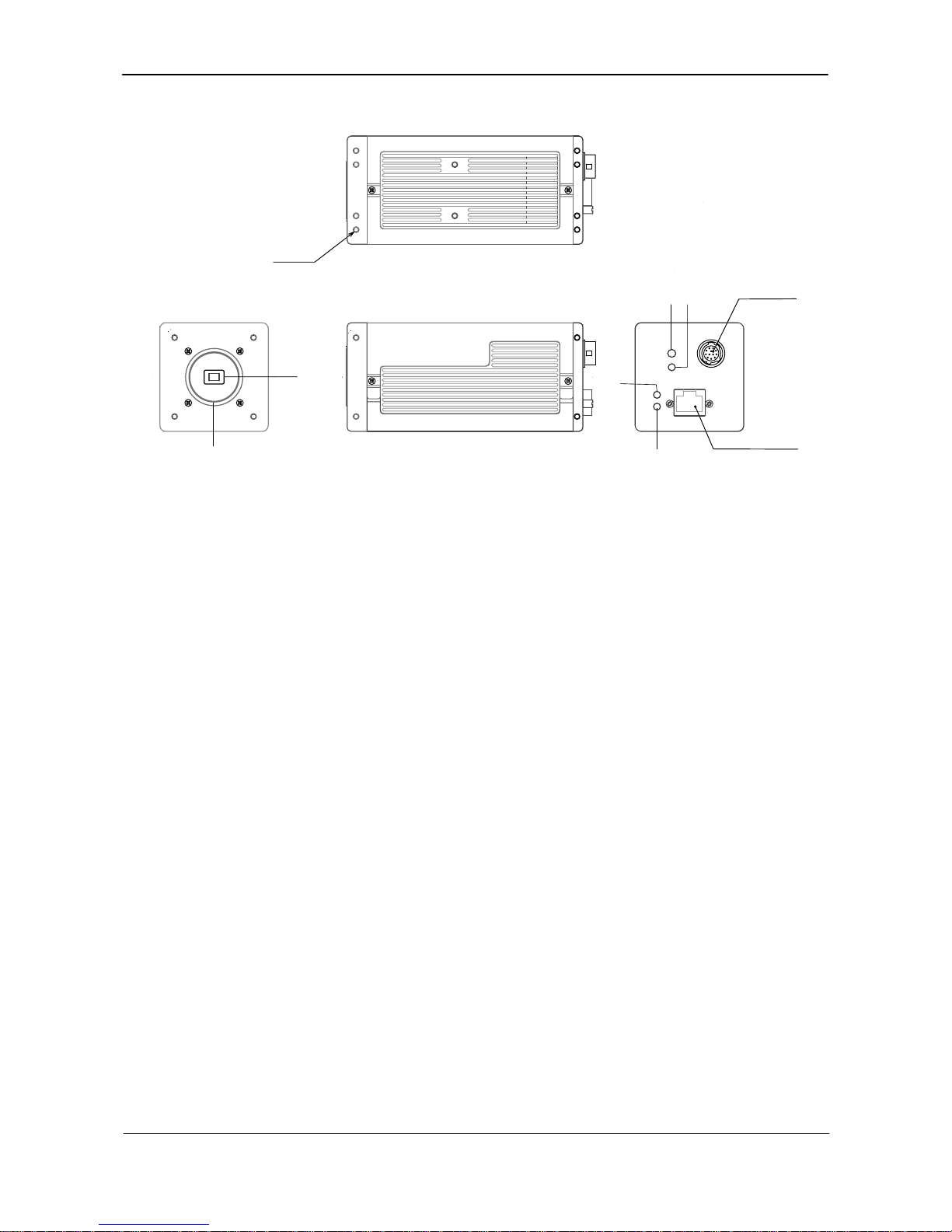
4. Locations and Functions
/ TRIG
DC IN
GigE
ACT.
LINK
W.B.
POWE R
/ TRIG
(depth0.2)
HIROSE 12pinConnector
8-M3depth5
HONDAGigabit-Ethernrt Jack
①
②
③
④
⑤⑥
⑦
⑧
⑨
1 Lens mount of C-mount type. *1)
2 RGB Prism with 3 x 1/3” CCD sensors
3 RJ45 GigE Connector
4 Hirose 12-pin connector for DC +12V power external sync signals
5 LED for power and trigger indication
Orange : Initialization after power ON
Green : Normal mode
Green flashing : Trigger pulse is being input
6 Switch for one-push white balance
7 LED for GigE network condition: LINK
8 LED for GigE network condition: ACT.
9 Mounting holes 8 x M3 depth 5mm .
*1) Note: Rear protrusion on C-mount lens must be less than 4.0mm
Fig. 1. Locations
Page 6
CV-M9 GE
- 5 -
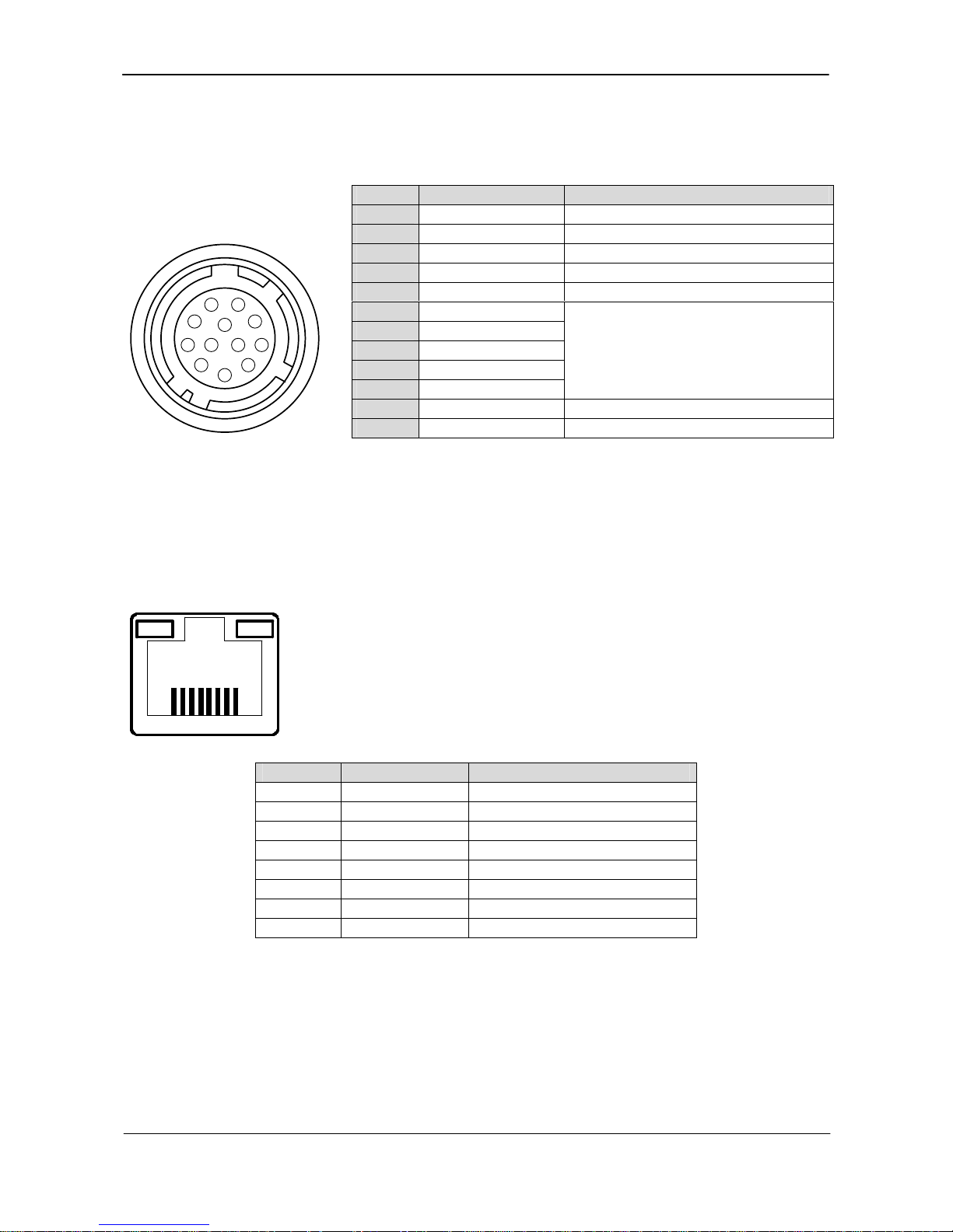
5. Pin Assignment
5.1. 12-pin Multi-connector (DC-in/GPIO/Iris Video)
Type: HR10A-10R-12PB-01
(Hirose) male.
Pin no.
Signal
Remarks
1 GND
2 +12 V DC input
3 GND
4 Iris video
Only for Continuous mode
5 GND
6 LVDS + / TTL IN 1
7 LVDS - / TTL IN 2
8 TTL OUT 1
9 TTL OUT 2
10 TTL IN
3
GPIO IN/OUT
11 +12 V DC input
12 GND
(Seen from rear of camera.)
3
4
5
6
7
8
9
10
11
12
1
2
Fig. 2. 12-pin connector.
5.2. Digital Output Connector for Gigabit Ethernet
RJ-45 Connector
12345678
Fig 3. Gigabit Ethernet connector
Pin No In/Out Name
1 In/Out MX1+ (DA+)
2 In/Out MX1- (DA-)
3 In/Out MX2+ (DB+)
4 In/Out MX3+ (DC+)
5 In/Out MX3- (DC-)
6 In/Out MX2- (DB-)
7 In/Out MX4+ (DD+)
8 In/Out MX4- (DD-)
Page 7
CV-M9 GE
- 6 -
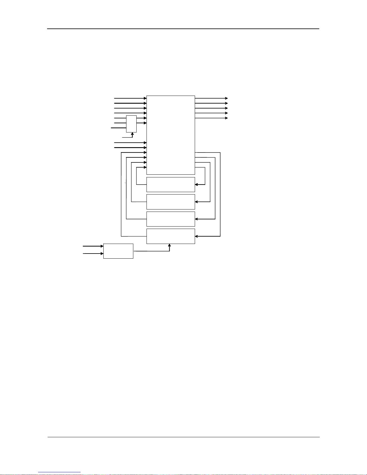
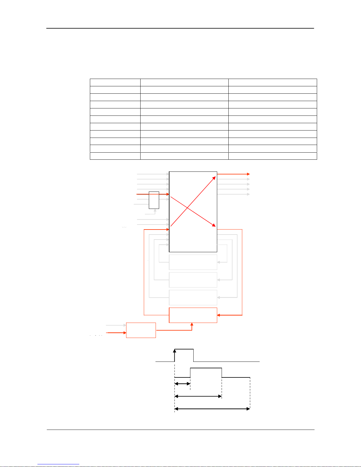
6. GPIO (Inputs and outputs)
6.1. Overview
All input and output signals pass through the GPIO (General Purpose Input and Output) module.
The GPIO module consists of a Look-Up Table (LUT – Cross-Point Switch), 4 Pulse Generators and
a 12-bit counter. In the LUT, the relationship between inputs, counters and outputs is governed
by internal register set-up.
LUT
(
Cross point switch)
LVAL IN
12bit
Counter
25MHz
Pixel Cloc
k
xTTL_LVDS Sel
DVAL IN
FVAL IN
EEN IN
HIROSE TTL IN 1
HIROSE TTL IN 2
LVDS IN
HIROSE TTL IN 3
Soft Trigger 0
Pulse Generator 3
(20bit Counter)
Pulse Generator 2
(20bit Counter)
Pulse Generator 1
(20bit Counter)
Pulse Generator 0
(20bit Counter)
CAMERA TRIGGER
CAMERA Ext. VD
CAMERA Ext. HD
HIROSE TTL OUT 1
HIROSE TTL OUT 2
LUT
(
Cross point switch)
LVAL IN
LVAL IN
12bit
Counter
25MHz
Pixel Cloc
k
xTTL_LVDS Sel
DVAL IN
DVAL IN
FVAL IN
FVAL IN
EEN IN
EEN IN
HIROSE TTL IN 1
HIROSE TTL IN 1
HIROSE TTL IN 2
HIROSE TTL IN 2
LVDS IN
LVDS IN
HIROSE TTL IN 3
HIROSE TTL IN 3
Soft Trigger 0
Soft Trigger 0
Pulse Generator 3
The blocks shown in the above diagram have the following functionality:
6.1.1. LUT (Look Up Table)
The LUT works as a cross-point switch which allows connecting inputs and outputs freely. The
signals LVAL_IN, DVAL_IN, FVAL_IN and EEN_IN all originate from the camera timing circuit. The
signal CAMERA_TRIGGER is connected to the camera timing circuit, allowing a hardware trigger.
6.1.2. 12-bit Counter
A 25MHz clock or the camera pixel clock can be used as a source. The counter has a “Divide by
N”, where N has the range 1 through 4096, allowing a wide range of clock frequencies to be
programmed.
6.1.3. Pulse Generators (0 to 3)
Each pulse generator consists of a 20bit counter. The behavior of these signals is defined by
their pulse width, start point and end point.
The pulse generator signals can be set in either triggered or periodic mode.
In triggered mode, the pulse is triggered by the rising edge/falling edge/high level or low level
of the input signal.
In periodic mode, the trigger continuously generates a signal that is based on the configured
pulse width, starting point and endpoint.
Page 8

CV-M9 GE
- 7 -
6.2. Inputs and outputs table
Signals I/O Description diagram
LVAL_IN I LVAL (Line Valid) from camera timing circuit
(See chapter 8.4 for timing relationship)
DVAL IN I DVAL from camera
FVAL_IN I FVAL (Frame Valid) from camera timing circuit
(See chapter 8.4 for timing relationship)
EEN_IN I EEN (Exposure Enable) from camera timing
circuit. (See chapter 8.4 for timing
relationship)
HIROSE_TTL_IN1 I TTL input on pin 6 of Hirose 12-pin.
Active when TTL is selected by xTTL_LVDS Sel
Fig. 4
HIROSE_TTL_IN2 I TTL input on pin 7 of Hirose 12-pin.
Active when TTL is selected by xTTL_LVDS Sel
Fig. 4
LVDS_IN I LVDS signal input on Hirose connector
LVDS + Pin 6 / LVDS – Pin 7
Active when LVDS is selected by xTTL_LVDS Sel
Fig. 5
HIROSE_TTL_IN3 I TTL input on pin 10 of Hirose 12-pin. Fig. 6
Soft_Trigger_0 I Software trigger input from Ethernet
Refer to GPIO module register xx
Pulse Generator out 0 I Pulse Generator 0 output
Pulse Generator out 1 I Pulse Generator 1 output
Pulse Generator out 2 I Pulse Generator 2 output
Pulse Generator out 3 I Pulse Generator 3 output
CAMERA TRIGGER O Trigger signal to camera timing circuit.
HIROSE TTL OUT 1 O TTL output on Pin 8 of Hirose 12-pin Fig. 7
HIROSE TTL OUT 2 O TTL output on Pin 9 of Hirose 12-pin Fig. 7
Pulse Generator in 0 O Pulse Generator 0 Clear input
Pulse Generator in 1 O Pulse Generator 1 Clear input
Pulse Generator in 2 O Pulse Generator 2 Clear input
Pulse Generator in 3 O Pulse Generator 3 Clear input
Page 9
CV-M9 GE
- 8 -
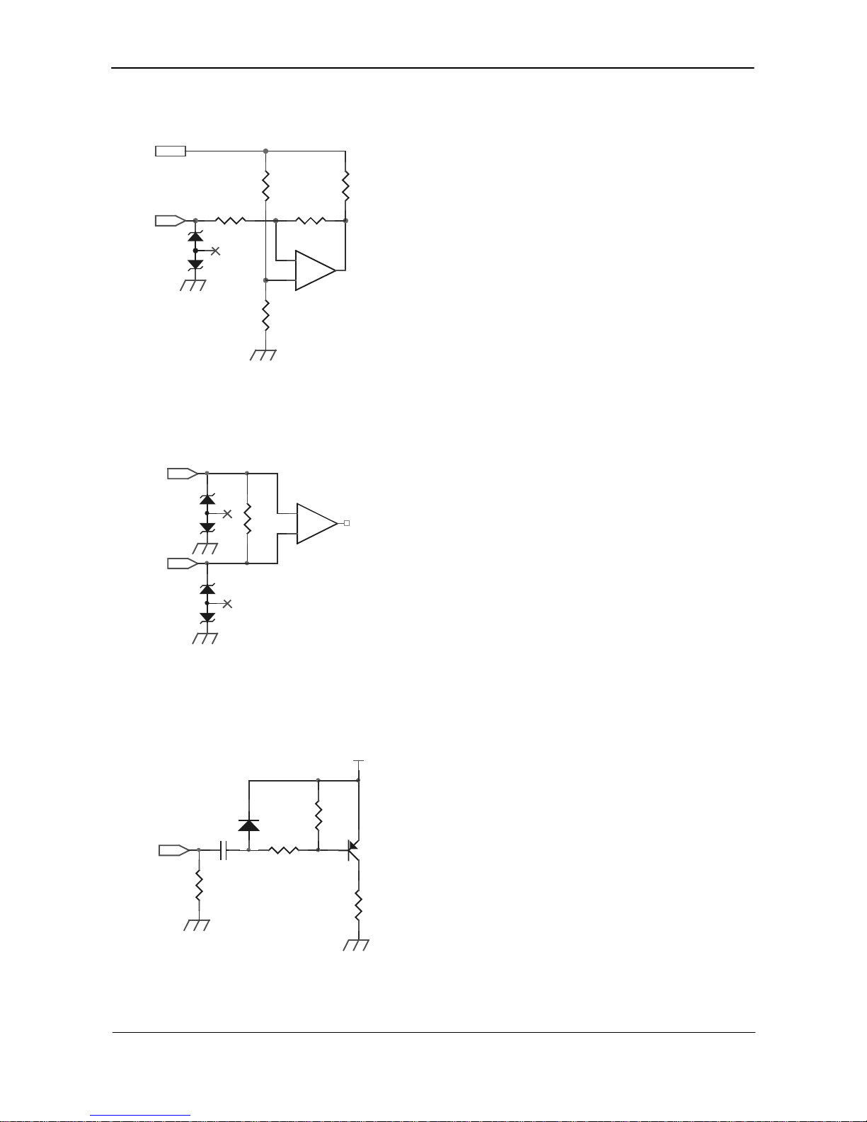
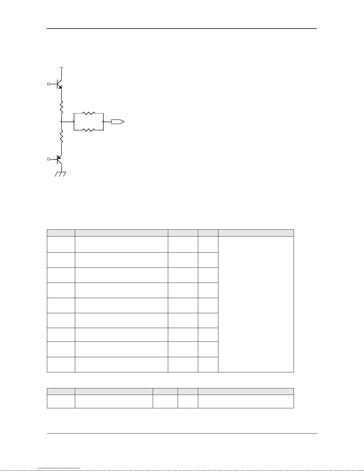
6.2.1. Equivalent circuit for TTL 1 and 2 inputs
This circuit is for TTL IN 1 and TTL IN 2 through
TTL_IN
+3.3V
R3
47K
R4
27K
R5
2.2K
R2
1M
-
+
U1A
D1
R1
1K
pins 6 and 7 at the 12-pin Hirose connector. It is a DCcoupled input.
See GPIO selector for setting this input (TTL or LVDS)
Fig.4 Hirose TTL IN (1 and 2) equivalent circuit
6.2.2. Equivalent circuit for LVDS input
This circuit is for LVDS IN – and + through pins 6 and 7 at
the 12-pin Hirose connector.
LVDS_IN+
LVDS_IN-
R1
100
D2
-
+
U1A
D1
See GPIO selector for setting this input (TTL or LVDS)
Fig.5 LVDS IN equivalent circuit
6.2.3. Equivalent circuit for TTL IN 3 Input
This circuit is for TTL IN 3 through pin 10 at the 12-pin
Hirose connector.
R1
1K
TTL_IN3
+5V
R4
1K
Q1
2
13
C1
0.1uF
D1
2
1
R2
1.2K
R3
15K
This circuit is AC coupled.
Fig.6 Hirose TTL IN 3 equivalent circuit
Page 10
CV-M9 GE
- 9 -
6.2.4. Equivalent circuit for TTL OUT 1 and 2 outputs
This circuit is for TTL OUT 1 and 2 through pins 8 and 9 at
the Hirose 12-pin connector.
+5V
Q1A
2
16
Q1B
5
4 3
R1
10
R2
10
R3 120
R4 150
TTL_OUT1
The output is sent from a 75 ohm source which is a
complementary Emitter-follower circuit.
The supply voltage for this circuit is 5V.
Fig.7 Hirose TTL OUT equivalent circuit
6.3. Configuring the GPIO module (register settings)
6.3.1. Signal Selector
Address Internal Name Access Size Value (Range)
0xB058 CAMERA TRIG Selector R/W 4
0xB05C CAMERA Ex. VD Selector R/W 4
0xB060 CAMERA Ex. HD Selector R/W 4
0xB064 HIROSE TTL OUT 1 Selector R/W 4
0xB068 HIROSE TTL OUT 2 Selector R/W 4
0xB06C Pulse Generator 0 Selector R/W 4
0xB070 Pulse Generator 1 Selector R/W 4
0xB074 Pulse Generator 2 Selector R/W 4
0xB078 Pulse Generator 3 Selector R/W 4
GPIO Selector:
0x00:CAMERA LVAL IN
0x01:CAMERA DVAL IN
0x02:CAMERA FVAL IN
0x03:CAMERA EEN IN
0x04:HIROSE TTL IN 1
0x05:HIROSE TTL IN 2
0x06:HIROSE TTL IN 3
0x07:HIROSE LVDS IN
0x09:SOFT TRIG 0
0x0D:Pulse Generator 0
0x0E:Pulse Generator 1
0x0F:Pulse Generator 2
0x10:Pulse Generator 3
0x7F:No Connect
Add 0x80 will result in low
active output.
6.3.2. xTTL_LVDS Selector
Address Internal Name Access Size Setting Value (and range)
0xA8B0 xTTL_LVDS Select R/W 4
0x00 : TTL In 1, TTL In 2 Active
0x01 : LVDS In Active
Page 11
CV-M9 GE
- 10 -
6.3.3. 12-bit counter
Address Internal Name Access Size Setting Value (and range)
0xB000 Clock source R/W 4
0: 25MHz
1: Pixel Clock
0xB004 Divide by N R/W 4
0x000: N=1
0x001: N=2
0x002: N=3
|
0xFFF: N=4096
6.3.4. Pulse generator (20 bit x 4)
There are 4 pulse generators (designated 0 through 3) that can be used to create various timing
scenarios by programming start point, endpoint, length and repeats.
Start Point
End Point
Length
Start Point
End Point
Length
Address Internal Name Access Size Setting Value (and range)
0xB008 Length Counter 0 R/W 4 0x00001 to 0xFFFFF
0xB00C Start point Counter 0 R/W 4 0x00000 to 0xFFFFF
0xB010 Repeat Count 0 R/W 4
0x00: infinite
0x01: 1 time
|
0xFF: 255 times
0xB014 End point Counter 0 R/W 4 0x00001 to 0xFFFFF
0xB018 Counter Clear 0 R/W 4
0: Free Run
1: High Level Clear
2: Low Level Clear
4: Rising Edge Clear
8: Falling Edge Clear
0xB01C Length Counter 1 R/W 4 0x00001 to 0xFFFFF
0xB020 Start point Counter 1 R/W 4 0x00000 to 0xFFFFF
0xB024 Repeat Count 1 R/W 4
0: Infinite
1: 1 time
|
255: 255 times
0xB028 End point Counter 1 R/W 4 0x00001 to 0xFFFFF
0xB02C Counter Clear 1 R/W 4
0x00: Free Run
0x01: High Level Clear
0x02: Low Level Clear
0x04: Rising Edge Clear
0x08: Falling Edge Clear
0xB030 Length Counter 2 R/W 4 0x00001 to 0xFFFFF
0xB034 Start point Counter 2 R/W 4 0x00000 to 0xFFFFF
Page 12
CV-M9 GE
- 11 -
Address Internal Name Access Size Setting Value (and range)
0xB038 Repeat Count 2 R/W 4
0x00: Infinite
0x01: 1 time
|
0xFF: 255 times
0xB03C End point Counter 2 R/W 4 0x00001 to 0xFFFFF
0xB040 Counter Clear 2 R/W 4
0x00: Free Run
0x01: High Level Clear
0x02: Low Level Clear
0x04: Rising Edge Clear
0x08: Falling Edge Clear
0xB044 Length Counter 3 R/W 4 0x00001 to 0xFFFFF
0xB048 Start point Counter 3 R/W 4 0x00000 to 0xFFFFF
0xB04C Repeat Count 3 R/W 4
0x00: Infinite
0x01: 1 time
|
0xFF: 255 times
0xB050 End point Counter 3 R/W 4 0x00001 to 0xFFFFF
0xB054 Counter Clear 3 R/W 4
0x00: Free Run
0x01: High Level Clear
0x02: Low Level Clear
0x04: Rising Edge Clear
0x08: Falling Edge Clear
Page 13
CV-M9 GE
- 12 -
6.4 GPIO programming examples
6.4.1 Trigger Phase Control
100clock delay to the input Trigger
Address
Registe
r
Value
0xA040 Trigger Mode 1 = EPS(Edge pre-select)
0xB000 Clock Choice 1 = Pixel Clock
0xB004 Counter Dividing Value 0 = Pass through
0xB008 Length Counter 0 1000 Clocks
0xB00C Start point Counter 0 100 Clocks
0xB010 Repeat Count 0 1
0xB014 End point Counter 0 500 Clocks
0xB018 Counter Clear 0 4 = Rising Edge Clear
0xB058 CAMERA TRIG Selector 13 = pulse generator 0
0xB06C Pulse Generator 0 Selector 4 = HIROSE TTL In 1
LVAL IN
xTTL_LVDS Select
DVAL IN
FVAL IN
EEN IN
HIROSE TTL IN 1
HIROSE TTL IN 2
LVDS IN
HIROSE TTL IN 3
Soft Trigger 0
LUT
(Cross point switch)
12bit
Counter
25MHz
Pixel Clock
Pulse Generator 3
(20bit Counter)
Pulse Generator 2
(20bit Counter)
Pulse Generator 1
(20bit Counter)
Pulse Generator 0
(20bit Counter)
CAMERA TRIGGER
CAMERA Ext. VD
CAMERA Ext. HD
HIROSE TTL OUT 1
HIROSE TTL OUT 2
LUT
(Cross point switch)
12bit
Counter
25MHz
Pixel Clock
Pulse Generator 3
(20bit Counter)
Pulse Generator 2
(20bit Counter)
Pulse Generator 1
(20bit Counter)
Pulse Generator 0
(20bit Counter)
CAMERA TRIGGER
CAMERA Ext. VD
CAMERA Ext. HD
HIROSE TTL OUT 1
HIROSE TTL OUT 2
HIROSE TTL IN 1
Pulse Generator 0
100
500
1000
output
HIROSE TTL IN 1
Pulse Generator 0
100
500
1000
output
Pulse Generator 0 timing
Page 14

CV-M9 GE
- 13 -
6.4.2 Internal Trigger Generator
Create a trigger signal and trigger the camera
Address
Registe
r
Value
0xA040 Trigger Mode 1 = EPS
0xB000 Clock Choice 1 = Pixel Clock
0xB004 Counter Dividing Value 963 = 1/964 dev(Line Rate)
0xB008 Length Counter 0 1000 Clocks
0xB00C Start point Counter 0 100 Clocks
0xB010 Repeat Count 0 0 = Free Run
0xB014 End point Counter 0 500 Clocks
0xB018 Counter Clear 0 0 = No Clear
0xB058 CAMERA TRIG Selector 13 = pulse generator 0
LUT
(Cross point switch)
LVAL IN
xTTL_LVDS Select
DVAL IN
FVAL IN
EEN IN
HIROSE TTL IN 1
HIROSE TTL IN 2
LVDS IN
HIROSE TTL IN 3
Soft Trigger 0
Pulse Generator 3
(20bit Counter)
Pulse Generator 2
(20bit Counter)
CAMERA TRIGGER
CAMERA Ext. VD
CAMERA Ext. HD
HIROSE TTL OUT 1
HIROSE TTL OUT 2
12bit
Counter
25MHz
Pixel Clock
Pulse Generator 1
(20bit Counter)
Pulse Generator 0
(20bit Counter)
Line Rate 37.5KHz
LUT
(Cross point switch)
LVAL IN
xTTL_LVDS Select
DVAL IN
FVAL IN
EEN IN
HIROSE TTL IN 1
HIROSE TTL IN 2
LVDS IN
HIROSE TTL IN 3
Soft Trigger 0
Pulse Generator 3
(20bit Counter)
Pulse Generator 2
(20bit Counter)
CAMERA TRIGGER
CAMERA Ext. VD
CAMERA Ext. HD
HIROSE TTL OUT 1
HIROSE TTL OUT 2
LUT
(Cross point switch)
LVAL IN
xTTL_LVDS Select
DVAL IN
FVAL IN
EEN IN
HIROSE TTL IN 1
HIROSE TTL IN 2
LVDS IN
HIROSE TTL IN 3
Soft Trigger 0
Pulse Generator 3
(20bit Counter)
Pulse Generator 2
(20bit Counter)
CAMERA TRIGGER
CAMERA Ext. VD
CAMERA Ext. HD
HIROSE TTL OUT 1
HIROSE TTL OUT 2
12bit
Counter
25MHz
Pixel Clock
Pulse Generator 1
(20bit Counter)
Pulse Generator 0
(20bit Counter)
Line Rate 37.5KHz
12bit
Counter
25MHz
Pixel Clock
Pulse Generator 1
(20bit Counter)
Pulse Generator 0
(20bit Counter)
Line Rate 37.5KHz
Pulse Generator 0
100 Line
500 Line
1000 Line
output
Pulse Generator 0
100 Line
500 Line
1000 Line
output
Pulse Generator 0 timing
Page 15
CV-M9 GE
- 14 -
6.4.3 Multi EEN Control with PWC
Camera EEN converts to 3 pulses and feed camera in PWC mode
Address
Registe
r
Value
0xA040 Trigger Mode 2 = PWC(Pulse width control)
0xB000 Clock Choice 1 = Pixel Clock
0xB004 Counter Dividing Value 963 = 1/964dev(Line Rate)
0xB008 Length Counter 0 1000 Clocks
0xB00C Start point Counter 0 100 Clocks
0xB010 Repeat Count 0 3 Cycles
0xB014 End point Counter 0 500 Clocks
0xB018 Counter Clear 0 1 = Level Low
0xB058 CAMERA TRIG Selector 4 = Hirose TTL IN 1
0xB06C Pulse Generator 0 Selector 3 = CAMERA EEN IN
CAMERA TRIGGER
CAMERA Ext. VD
CAMERA Ext. HD
HIROSE TTL OUT 1
HIROSE TTL OUT 2
LUT
(Cross point switch)
LVAL IN
12bit
Counter
25MHz
Pixel Clock
xTTL_LVDS Select
DVAL IN
FVAL IN
EEN IN
HIROSE TTL IN 1
HIROSE TTL IN 2
LVDS IN
HIROSE TTL IN 3
Soft Trigger 0
Pulse Generator 3
(20bit Counter)
Pulse Generator 2
(20bit Counter)
Pulse Generator 1
(20bit Counter)
Pulse Generator 0
(20bit Counter)
Line Rate 37.5KHz
CAMERA TRIGGER
CAMERA Ext. VD
CAMERA Ext. HD
HIROSE TTL OUT 1
HIROSE TTL OUT 2
CAMERA TRIGGER
CAMERA Ext. VD
CAMERA Ext. HD
HIROSE TTL OUT 1
HIROSE TTL OUT 2
LUT
(Cross point switch)
LVAL IN
12bit
Counter
25MHz
Pixel Clock
xTTL_LVDS Select
DVAL IN
FVAL IN
EEN IN
HIROSE TTL IN 1
HIROSE TTL IN 2
LVDS IN
HIROSE TTL IN 3
Soft Trigger 0
Pulse Generator 3
(20bit Counter)
Pulse Generator 2
(20bit Counter)
Pulse Generator 1
(20bit Counter)
Pulse Generator 0
(20bit Counter)
Line Rate 37.5KHz
EEN
IN
500
1000
output
EEN
IN
500
1000
output
Pulse Generator 0 timing
Page 16
CV-M9 GE
- 15 -
7. GigE Vision Streaming Protocol (GVSP)
7.1. Digital Video Output (Bit Allocation)
Although the CV-M9GE is a digital camera, the image is generated by an analog component, the
CCD sensor. There are three CCD sensors in this camera. One for each R, G and B channel.
The table and diagram below show the relationship between the analog CCD output level and
the digital output.
CCD out Analog Signal * Digital Out(30bit) Digital Out(24bit)
Black Setup 3.6%, 25mV 32LSB 8LSB
200mV 700mV 890LSB 222LSB
230mV 800mV 1023LSB 255LSB
Ana log S igna l [mV ]
B lack Leve l
1023
890
32
0
25
700
D ig i ta l Ou t [LSB ]
Wh i te C l ip Leve l
100%Level
800
The standard setting for 10-bit video level is 890 LSB. For 8-bit, the standard setting is 222 LSB.
200 mV CCD output level, 100% video output.
Fig.8 Digital Output
7.2. Bit Allocation (Pixel Format / Pixel Type)
In the GigE Vision Interface, GVSP (GigE Vision Streaming Protocol) is used for an application
layer protocol relying on the UDP transport layer protocol. It allows an application to receive
image data, image information and other information from a device.
In CV-M9GE, the following pixel types supported by GVSP are available.
With regard to the details of GVSP, please refer to the GigE Vision Specification available from
AIA.
7.2.1. GVSP_PIX_BGR10V1_PACKED (32bit)
1Byte 2Byte 3Byte 4Byte
RRGGBBXXBBBBBBBBGGGGGGGGRRRRRRRR
Little Endian Bit Alignment
7.2.2. GVSP_PIX_BGR10V2_PACKED (32bit)
1Byte 2Byte 3Byte 4Byte
RRRRRRRRRRGGGGGGGGGGBBBBBBBBBBXX
Little Endian Bit Alignment
7.2.3. GVSP_PIX_RGB8_PACKED (24bit)
1Byte 目 2Byte 目 3Byte 目
RRRRRRRRGGGGGGGGBBBBBB B B
Page 17

CV-M9 GE
- 16 -
Little Endian Bit Alignment
Address Internal Name Access Size Value
0xA410 Pixel Format type R/W 4
0x0220001C:BGR10V1 Packed
0x0220001D:BGR10V2 Packed
0x02180014:RGB8 Packed
8. Functions and Operations
8.1. GigE Vision Standard Interface
The CV-M9 GE is designed in accordance with the GigE Vision standard. In transmits digital
images over CAT5e or Cat6 Ethernet cables. All camera functions are also controlled via the GigE
Vision interface.
The camera can operate in a continuous mode, providing an endless stream of images. For
capturing individual images, related to a specific event, the camera can also be trigged. For
precise triggering, it is recommended to use a hardware trigger applied to the Hirose 12-pin
connector. It is also possible to initiate a software trigger through the GigE Vision interface.
However, when using software trigger, certain latency inherent to the GigE interface must be
anticipated. This latency, that manifests itself as jitter, greatly depends on the general
conditions and traffic on the GigE connection. The frame rate described in this manual is for the
ideal case and may deteriorate depending on conditions.
8.2. Recommended Network Configurations
Although the CV-M9GE conforms to Gigabit Ethernet (IEEE 802.3) not all combinations of network
interface cards (NICs) and Switches/Routers are suitable for use with the GigE Vision compliant
camera.
JAI will endeavor to continuously verify these combinations, in order to give users the widest
choice of GigE components for their system design.
8.2.1 Verified Network Interface Cards (NICs)
At the time of publishing this document these combinations have been verified:
NIC manufacturer Model PCI Bus PCI-X Bus PCI-Express Bus
Intel PRO/1000MT
(PWLA8490MT)
√ (33MHz) √(100MHz)
−
Intel PRO/1000GT
(PWLA8391GT)
√ (33MHz) √ (33MHz)
−
Intel PRO/1000PT
(EXPI9300PT)
− −
√ ( x1 )
Minimum PC requirements are as follows in order to fulfill the above conditions:
IntelP4 2.8G(HT) or better, alternatively AMD Athlon 64 x2, CPU
At least 1 GB memory
More than 200 GB free disk space
Windows XP, SP2(32bit)
Optimized filter driver included in the JAI SDK Light
Page 18

CV-M9 GE
- 17 -
To ensure the integrity of packets transmitted from the camera is recommended to follow these
simple guidelines:
1. Whenever possible use a peer-to-peer network.
2. When connecting several cameras going though a network switch, make sure it is capable
of handling jumbo packets and that it has sufficient memory capacity.
3. Configure inter-packet delay to avoid congestion in networks switches.
4. Disable screen saver and power save functions on computers.
5. Use high performance computers with multi-CPU, hyper-thread and 64-bit CPU, etc.
6. Only used Gigabit Ethernet equipment and components together with the camera.
7. Use at least Cat5e or preferably Cat6 Ethernet cables.
8. Whenever possible, limit the camera output to 24-bit.
Video bit rate for CV-M9GE is:
24 bit pixel format (GVSP_PIX_RGB8) 566 M bit/s
(1024(H) x 768(V) x30(Frame) x 24(bit))
30 bit pixel format (GVSP_PIX_RGBVD) 755 M bit/s
(1024(H) x 768(V) x30(Frame) x 30(bit))
However, as the UPD Packet Header is added, the real bit rate will increase by 10%.
8.3. Basic functions
A 16-bit processor controls all functions in the CV-M9GE camera. The CCD sensor output is
normalized in preamplifiers. The signals are then digitized to 12 bits. Digital gain control and
look-up tables perform signal processing in 12-bits before it is truncated to a 10 or 8 bit for BGR
GigE Vision standard packet format.
A/D
A/D
A/D
16 bit digital processing
12 bit
B
R
G
Prism
Timing
A. gain D. Gain
Shading
map
Knee
Point
slope
12 bit 10 bit
Iris video
RGB input
Shading
data
A/D
A/D
A/D
16 bit digital processing
12 bit
B
R
G
Prism
Timing
A. gain D. Gain
Shading
map
Knee
Point
slope
12 bit 10 bit
Iris video
RGB input
Shading
data
GigE
Cont
roller
RGB 3x8bit signal
RGB 3x10bit signal
12P
RJ-45
Fig. 9. Principle diagram for signal processing
8.3.1. White Balance (by gain setting)
By adjusting the R and B gain settings, it is possible to have correct color balance in the video
output. A white scene will be shown as a white image. This white balance can be done in
different ways:
(1) Manual white balance (user adjusts gain settings)
(2) One-push automatic white balance
(3) Continuous (tracking) automatic white balance
(4) Pre-defined color temperature settings: 3200K (factory default), 4600K and 5600K.
The register 0xA0C0 is used to select the function.
Page 19

CV-M9 GE
- 18 -
Manual white balance
By adjusting the Red (Register 0xA0C8); Blue (Register 0xA0CC) and Master Gain (Register
0xA0C4) gains settings, it is possible to achieve a proper white balance output from the camera
for a wide range of color temperatures. The recommended method is to point the camera at a
white target, and adjust gain settings until image on the screen matches the target.
One-push white balance. (Set register 0xA0D0 to 0x00)
If this register is set, an automatic white balance is performed once. To use this function the
camera must be operating in the continuous mode.
The result of this function (0 = complete; 1 = too dark; 2 = too bright; 3 = timeout; 4 = busy; 5 =
out of range; 6 = trigger mode not set to continuous) can be read out of register 0xA0D8.
Please see the register map for complete details of the register settings and responses.
lower rightlower middlelower left
middle rightmiddlemiddle left
upper rightupper middleupper left
lower rightlower middlelower left
middle rightmiddlemiddle left
upper rightupper middleupper left
FullFull
0
12
3
45 6
789
Set Auto White Balance area.
With this function it is possible to select which part of
the image the automatic white balance function uses to
calculate the gain settings.
The register 0xA0D4 is used to set this function.
Fig. 10. Auto white balance areas.
8.3.2. White balance (by individual R, G and B channel shutter settings)
In order to achieve proper white balance without compromising signal-to-noise ratio, it is
possible to adjust the exposure (shutter) time of each R, G and B channel individually. Please
see chapter 8.3.6. Electronic Shutter for details on how to set this function.
8.3.3. Automatic Dynamic shading correction
The CV-M9GE camera has a digital shading correction circuit, which can compensate for prism
chromatic shading, for lens shading and for CCD shading. It makes the choice of lenses wider.
The camera with a given lens and a given f-number is looking on a homogeneous white scene.
A horizontal profile of the shading in 128 points is made for the 3 colors.
A vertical profile of the shading in 96 points is
made for the 3 colors. The average level of each
divisions for R,G and B respectively is compared
with the level of the image centre and the level
difference compensates the video data. The
resulting image is then compensated for shading
caused by the lens, prism and CCD.
0 127
0
95
H shading data
V
shading
data
0 127
0
95
H shading data
V
shading
data
Fig. 11. Dynamic shading correction.
The factory setting is done with a Fujinon 15mm F2.2 lens, with the iris is set to F5.6.
Note: Lens requirements.
Although the shading correction widens the choice of lenses for this camera, it is recommended
to use lenses designed for 1/3” 3 CCD cameras to obtain the best image quality. As chromatic
shading depends of the focal length and the iris setting of the lens, avoid using wide-angle
lenses, and working with the lens iris setting fully open.
Page 20

CV-M9 GE
- 19 -
8.3.4. Knee function
The video signal is digitized to 3x12-bit
and the most significant 3x8 or 3x10-bit
are presented at the output. By using a
look-up table function it is possible to
compress the video signal to change the
dynamic range. It can be done
individually for R, G and B with the Knee
Function.
Output Camer a Li nk D at a Level
1023
890
0
0 4095
Input CCD Data Level
2848
Knee Point = 37Ah (890)
Knee Slope = 080h (1/16)
In this case : Maximum Value is 968 LSB.
968
[100%]
32
[0%]
Knee Point
1279
102
1/16
Fig. 12. Knee function.
The Knee Function is given by 2 sets of
parameters. Knee point and slope. These
2 sets of data determine the relationship
between output and input data. This
conversion is done in hardware (FPGA)
using the knee data.
The normal transfer function is with a
slope 1:1. From a given point and up, the
slope can be changed. This point is the knee point
parameter, and its range is from 0 to 1023 referring to the video output.
The factory setting is 890.
The new slope can be set from 1:0 to 1:2.
A slope 1:0 is a clipper function, which will limit the output signal. A slope 1:2 will function as a
2 times contrast expanding function.
The slope parameter range is from 0 to 4095.
0 is slope 1:0.
2048 is slope 1:1.
4095 is slope 1:2.
The factory setting is 800, giving a slope of 800/2048 =1:0.39. All of the above is based on 3x10bit output.
8.3.5. ROI (Region of Interest)
The CV-M9GE allows two ROIs to be set. The ROI must not be overlapped.
The following is a matrix chart for ROI and Trigger modes. Please note that "ROI 2" and "ROI 1 +
ROI 2" is not a standard GenICam function.
For setting ROIs, use registers 0xA41C through 0xA43C.
Trigger Mode ROI 1 ROI 2 ROI 1 + ROI 2
EPS Trigger Yes Yes Yes
PWC Trigger Yes Yes Yes
Sequential EPS Trigger Yes (Note1) No No
Sequential PWC Trigger Yes (Note1) No No
EPS Trigger Delayed Readout Yes No No
PWC Trigger Delayed Readout Yes No No
Sequential EPS Trigger Delayed Readout Yes (Note1) No No
Sequential PWC Trigger Delayed Readout Yes (Note1) No No
Note 1: ROI 1 setting for "Sequential" must use registers 0xA808 through 0xA8A4 on register map.
Page 21

CV-M9 GE
- 20 -
8.3.6. Electronic Shutter
The CV-M9GE has two conventional shutter functions, Preset Shutter and Programmable
Exposure, as well as the GenICam standard “Exposure Time Abs” function:
Preset shutter (Register 0xA004)
12 pre-set (fixed) shutter speeds, OFF (1/30); 1/60; 1/100; 1/120; 1/250; 1/500; 1/1,000;
1/2,000; 1/4,000; 1/10,000; 1/16,000 and 1/50,000, can be selected by this function.
Programmable Exposure (Register 0xA008 - common setting)
The shutter speed can be set by 1L increments in the range of 0.5L to 791L. 791L corresponds to
shutter OFF (1/30). L=42.07µs (line period) for full frame and partial scan.
Programmable Exposure (Registers 0xA00C [Red], 0xA010 [Green] and 0xA010 [Blue])
Individual shutter settings for R, G or B channels are available for Continuous and Edge PreSelect (EPS) trigger modes only.
The actual exposure time should add 0.5L in addition to setting lines number due to 0.5L
overhead in the range of 0L to 790 L.
Shutter speed (Time) for Trigger Mode
Minimum exposure time Max. exposure time
Normal
Partial
20μs
Continuous
and EPS
V-Binning
30μs
1 Frame(note 1)
Normal
Partial
42.07μs×2L+20μs(0.5L) = 66.7μs
( ≈ 1/10,000s)
PWC
V-Binning
50.96μs×2L+30.μs(0.5L) = 131.7μs
(≈ 1/8,000s)
60 Frame
(Note 1 )
Note1): The maximum shutter time depends on total lines of each read out system.
Exposure time for Normal Readout = PE(Line) x 1H(42.07us) + 20us (PE=0~791)
Exposure time for 1/2 Partial Readout = PE(Line) x 1H(42.07us) + 20us (PE=0~491)
Exposure time for 1/4 Partial Readout = PE(Line) x 1H(42.07us) + 20us (PE=0~347)
Exposure time for 1/8 Partial Readout = PE(Line) x 1H(42.07us) + 20us (PE=0~275)
Exposure time for V-Binning Readout = PE(Line) x 1H(50.96us) + 30us (PE=0~395)
Exposure Time Abs (Register 0xA054)
This is a function specified in the GenICam standard.
The shutter speed can be entered as an absolute exposure time in microseconds (μs) in register
address 0xA054. The entered absolute time (Time Abs) is then converted to programmable
exposure (PE) value inside the camera.
In this mode, the minimum exposure time is 20 µs and then after, the shutter value is changed
by 42 µs increment.
The relation with PE value is:
PE = INT (Exposure time / 42) for Normal Readout, 1/2 Partial to 1/8 Partial mode
PE = INT (Exposure time / 51) for V-Binning Readout mode
Note: “INT” means integer (truncated).
Page 22

CV-M9 GE
- 21 -
Shutter and Mode matrix
Preset Programmable
RGB common RGB individual RGB common RGB individual
Continuous
Yes -
Yes Yes
EPS
Yes - Yes Yes
PWC - -
-
-
8.3.7. Color bar for test
8222822282228222
Blue
8888222222222222
Green
8822222288222222
Red
8222822282228222
Blue
8888222222222222
Green
8822222288222222
Red
Values
in 8 bit
32890328903289032890
Blue
32323232888890890890
Green
32328908903232890890
Red
32890328903289032890
Blue
32323232888890890890
Green
32328908903232890890
Red
Values
in 10 bit
The CV-M9GE camera has a build in color bar
generator. When it is activated, the output image
will be as shown below. The RGB values are shown
for both 8 and 10 bit output.
Fig. 13. Color bar RGB values
8.3.8. Analogue output for Auto Iris Lens
This signal is available only for the continuous mode.
The signal is fed from CCD output and therefore the
setting of camera gain does not affect this output.
The video signal does not include composite sync and
the output level is 0.7 V p-p with 75 ohms output
impedance.
0
100%Level700
200
Ana log Ou t [mV ]
CCDOut [mV ] 265
930
Fig.14 Lens Iris Analogue output
Page 23

CV-M9 GE
- 22 -
8.4. Sensor Layout and timing
8.4.1. CCD Sensor Layout
Active Pixels
1024(H)x768(V)
Optical
Black
Lines
ptical B lack Lines
Rese
r
ved Lines
Rese
r
ved Lines
1024
29 3 5 5 4
6
2
5
dumm
k
b
lank
1420 Clock
Read
Read
Out
(Ve rtical)
343
1077
788
768
792
y
Fig. 15. CCD sensor layout
Important Note: In GigE Vision, only Active Pixel Area is output through the GigE interface.
Dummy, optical black and reserved areas are not output.
Table for scanning.
The below table shows the start line, the stop line and the number of active lines in the
vertically centered area of the CCD sensor. The front and back lines are the lines used for the
fast dump readout in partial scanning mode.
Scanning
Start
line #
End
line #
Active
lines
Front
lines
Back
lines
Blank
lines Remarks
Full 1 768 768 12 8 4
Partial 1/2 192 576 384 54 50 4
Partial 1/4 288 480 192 78 74 4
Partial 1/8 336 432 96 90 86 4
V. Binning 1/2 767/768
384 5 4 3
Note:
The following pages show the timing chart for Full, Partial and Vertical binning readout modes.
These timing charts describe internal camera timing and the output through Gigabit Ethernet.
Only the active lines, i.e. 768 lines for full scanning, are output.
Page 24

CV-M9 GE
- 23 -
8.4.2. Horizontal timing
(20us)
86ck
8ck
45ck
5ck
5ck
29ck
29ck
167
590ck
676ck
92
86
343ck
1420ck
1077ck
1328ck
1024ck
1077ck
343ck
3ck
40ck
1024ck
3ck
343ck
(Hirose 12pin)
Exposure
Period
Dummy+
Blank
5ck
DATA OUT
DVAL
CCD Out
Effective Pixels
FVAL
SUB
SG
EEN
FVAL Falling Edge
1LVAL period
1ck = 33.750MHz (29.63ns/ck)
FVAL Raising Edge
LVA L
XEEN
OB
Reserved
OB
Reserved
Fig. 16. Horizontal timing
8.4.3. Vertical timing
2L6L 4L
7L 5L
768L
Effective Lines
7
6
5
7
6
4
7
6
6
7
6
8
7
6
7
R
es
er
v
e
d
12345
Rese rved
OB
BlankOB
DATA OUT
DVAL
4L788L
792L
0.5L
LVAL
SUB
SG
FVAL
EEN
FVAL
LVAL
1FVALperiod
Exposu re
Pe r iod
1L = 1420C lo ck (42 .07u s )
XEEN
(Hirose12pin)
Fig. 17. Vertical timing for full scan
Page 25

CV-M9 GE
- 24 -
8.4.4. Partial Scanning
Dummy
3L 4L384L1
123
3
8
1
3
8
0
3
8
2
3
8
4
3
8
3
Effect ive Lines
4
DVAL
DATA OUT
5
OB
A
50L (1 /2 )
B
50L (1 /2 )
C
54L
492L
488L 4L
0.5L
Back o f F rame
LVAL
SUB
SG
FVAL
EEN
Exposu re
Pe r iod
H igh Speed
Transfer
Front of Frame
B
la
n
k
XEEN
(H i rose 12p in )
1L= 1420Clock (42.07us)
1L = 42.07 μs
Fig. 18 Vertical timing for 1/2 partial scan
Dummy
1
8
9
1
8
8
1
9
0
1
9
2
1
9
1
Effect ive Lines
45
123
DVA L
DATA OUT
OB3L 74L192L1 4L
78L
74L
Bl
a
n
k
Back o f F rameFront of Frame
1FVAL period
LVA L
SUB
FVAL
EEN
Exposure
Pe r iod
SG
H igh Speed
Transfer
344L
348L
4L
0.5L
XEEN
(Hirose12pin)
1L ine = 1420C lo ck (42 .07us )
Fig. 19 Vertical timing for 1/4 partial scan
Page 26

CV-M9 GE
- 25 -
9
3
9
2
9
4
9
6
9
5
Effective Lines
45
123
DVAL
DATA OUT
86L3L 86L 4L1 96L
OB
90L
Bl
a
n
k
Back o f F rame
1FVALperiod
Front of Frame
LVAL
SUB
SG
FVAL
EEN
Exposure
Pe r iod
High Speed
Transfer
276L
272L
0.5L
4L
XEEN
(Hirose12pin)
1L ine = 1420C lo ck (42 .07us )
Fig. 20 Vertical timing for 1/8 partial scan
8.4.5. Vertical binning
DATA OUT
DVAL
CCD O u t
E f fec t ive P ixe ls
(30us )
FVAL
SUB
SG
EEN
FVAL Fa l l ing Edge
1LVALperiod
1ck = 33 .750MHz (29 .63ns /ck )
FVAL Ra is ing Edge
LVAL
XEEN
(Hirose 12pin)
Exposure
Pe r iod
643
1720
1077
1024
1024
1077 643
86
1628
86ck
Dummy+
BlankRese rved
8ck 45ck
467
927
1013
OB R e se r ve d
3ck 5ck
OB
40ck
643 5ck3ck
5ck
29ck
29ck
92
Fig.21 Horizontal timing for V binning.
Page 27

CV-M9 GE
- 26 -
12345
DATA OUT
DVAL
OB Effective Lines
2L3L 1L
3
8
1
3
8
0
3
8
2
3
8
4
3
8
3
3L384L
4L
0.5L
LVAL
FVAL
EEN
Exposure
Pe r iod
SG
SUB
LVAL
FVA L
1FVALPeriod
392L
396L
Rese
r
ved
R
e
s
er
v
e
d
XEEN
(Hirose12pin)
Fig. 22. Vertical timing for V binning.
Page 28

CV-M9 GE
- 27 -
8.5. Operation Modes
This camera can operate in 5 primary modes.
1. Continuous Mode Pre-selected exposure.
2. Edge Pre-select Mode (EPS) Pre-selected exposure.
3. Pulse Width Control Mode (PWC) Pulse width controlled exposure.
4. Sequential Trigger Pre-selected exposure (EPS)
5. Delayed Readout Trigger Pre-selected exposure (EPS/PWC)
The triggered accumulation in EPS, PWC, Sequential Trigger and Delayed Readout Trigger can be
LVAL synchronous or LVAL a-synchronous.
In LVAL synchronous accumulation, a new exposure can be started while the previous frame is
read out. The new exposure should not be finished before the frame is read out. FVAL (Trigger
Duration) shall be low for >2 LVAL. The maximum frame rate in trigger modes can then be close
to the frame rate in continuous mode.
The minimum trigger interval should be longer than (1 FVAL+1 LVAL) in the case of Smear Less
OFF and Same RGB exposure time.
In LVAL a-synchronous accumulation, a new trigger must not be applied before the previous
frame is read out. (FVAL is low).
The minimum trigger interval should be longer than (exposure time + 1 FVAL+1 LVAL).
Refer to chapter 8.5.1. and 8.5.2. for accumulation details.
8.5.1. LVAL synchronous accumulation
In LVAL accumulation mode, the accumulation will start synchronously with LVAL. The trigger
pulse should be longer than 2 LVAL (LVAL=42.07µs). The accumulation will start at the first LVAL
after the trigger leading edge. The exposure start delay will be up to 1 line. (42.07 μsec.).
In EPS mode the exposure stops 0.5 L after the selected shutter time, (in number of LVAL).
In PWC mode the exposure stops 0.5 L after the first LVAL after the trigger trailing edge. It
results in up to 1 LVAL jitter.
In trigger modes with LVAL synchronous accumulation, a new exposure can be started while the
previous frame is read out. The new exposure should not finish before the frame is read out.
FVAL (Trigger Duration) shall be low for >2 LVAL. The maximum frame rate in trigger modes can
then be close to the frame rate in continuous mode.
Minimum trigger interval≥ (1 FVAL + 1 LVAL). (EPS mode)
note: Smear-less OFF / Common exposure time for RGB
Page 29

CV-M9 GE
- 28 -
Edge Pre-Select Mode : Full Frame
Ex p o s u r e De l ay
1. 5L
Dat a out Del ay
( Exposur e)
DATA out
t1+1L(Max)
13. 5L
Ex t . Tr i g
FVAL
EEN
LVAL
Ex p o s u r e Pr i o d
XEEN
(Hi r o se 12pi n)
1L =
1420Cl ock ( 42. 07us)
Fig. 23. LVAL synchronous accumulation in EPS mode
Pulse Width Control Mode : Full Frame
1.5L
Da ta ou t De l ay
De la y o f E xpos u r e S ta r t
(Exposure)
DATA ou t
t1+1L (Ma x )
13 .5L
Ex t .T r ig
FVA L
EEN
LVA L
Exposu re P r iod
Pu l seW id th Con t ro l mode の例 (Fu l l F rame )
De la y o f E xpos u r e End
0.5 to 1.5L
XEEN
(H i rose 12p in )
1L = 1420C loc k (42 .07us )
Fig. 24. LVAL synchronous accumulation in PWC mode
Page 30

CV-M9 GE
- 29 -
8.5.2. LVAL a-synchronous accumulation
In LVAL a-synchronous mode, the accumulation will start immediately after the trigger leading
edge. The exposure start delay is 9.7 μsec. (In V-binning mode, this delay will be 39.7 μsec)
In EPS mode the exposure stops 0.5 L after the selected shutter time, (in number of LVAL).
In PWC mode the exposure stops 29.7μsec after the trigger trailing edge.
A new trigger must not be applied before the previous frame is read out. (FVAL is low).
Minimum trigger interval ≥ (exposure time + 1 FVAL + 1 LVAL). (EPS mode)
Edge Pre-select Mode : Full Frame
Exposure De lay
(Exposure)
DATA ou t
Da ta ou t De lay
Edge P re -Se lec t mode の例 (Fu l l F rame )
1to2L
13 to 14L
Ex t .T r ig
FVA L
EEN
LVA L
Exposu re P r iod
1L = 1420c loc k (42 .07u s )
9.7us
XEEN
(H i rose 12p in )
Fig. 25. LVAL a-synchronous accumulation in EPS mode
Pulse Width Control Mode : Full Frame
Da ta ou t De lay
De la y o f E xpo su r e S ta r t
(Exposure)
DATA ou t
1to2L
13 to 14 L
Ex t .T r ig
FVA L
EEN
LVA L
Exposu re P r iod
De la y o f E xpo su r e End
XEEN
(Hirose 12pin)
1L = 1420c lo ck (42 .07u s )Pu l seW id th Con t ro l mode の例 (Fu l l F rame )
9.7us
29 .7u s
Fig. 26. LVAL a-synchronous accumulation in PWC mode
Note: In V-Binning mode, the delay of exposure end is 39.7μs (1L=1720 clk)
Page 31

CV-M9 GE
- 30 -
8.5.3. Continuous operation
For applications not requiring asynchronous external trigger, but where a continuous stream of
images is required, this mode should be used.
In this mode it possible to use an auto-iris lens (video drive). The CV-M9GE provides an auto-iris
lens video signal at pin 4 of the 12-pin Hirose connector.
For timing details, refer to fig. 16. through fig. 22.
To use this mode:
Set function: Trigger mode Continuous
Scanning Full, Partial scanning
Vertical binning On/Off
Shutter mode Preset, Programmable
Shutter speed or
Programmable exposure
8.5.4. Edge Pre-select Trigger Mode
An external trigger pulse initiates the capture, and the exposure time (accumulation time) is the
fixed shutter speed set by registers. The accumulation can be LVAL synchronous or LVAL asynchronous.
The resulting video signal will start to be read out after the selected shutter time.
For timing details, refer to fig. 16. through fig. 22. and fig. 27.
To use this mode:
Set function: Trigger mode EPS
Scanning Full, Partial
Vertical binning ON / OFF
Shutter mode Preset, Programmable
Shutter speed
Programmable exposure
Accumulation LVAL Sync / LVAL a-sync
Other functions and settings
Input: Ext. trigger. Gigabit Ethernet or 12-pin Hirose
Important notes on using this mode
Trigger pulse >2 LVAL to <1 FVAL)
Minimum trigger interval in synchronous accumulation mode
In case R,G and B exposure is common :
≥ (1 FVAL(792L) + 1 LVAL)
In case R,G and B exposure is individual :
≥ (Max. Exp. time – Min. Exp. time) + 1 FVAL (792L) + 1 LVAL
Minimum trigger interval in a-synchronous accumulation mode
≥ ( exposure time + 1 FVAL(792L) + 1 LVAL).
Minimum trigger interval in Smear-less ON:
≥ (Smear-less time (198L) + Max. Exp. time + 1FVAL(792L) + 1 LVAL
Minimum trigger interval with Sequential Mode together
In case the same R,G and B shutter value for all sequences, and SYNC mode
≥ 1 FVAL (792L) + 1L
In case the same shutter for each sequence, ( SYNC/a-SYNC )
≥ Maximum Exposure + 1 FVAL (792L) + 1L
In case the different shutter for R,G and B, ( SYNC/a-SYNC )
≥ (Max. Exp. time – Min. Exp. time) + 1 FVAL (792L) + 4 LVA
Page 32

CV-M9 GE
- 31 -
In EPS trigger mode, R, G and B exposure can be set individually. Provided the gain in each
channel is set to the same value, this function allows white balance to be achieved with
the same noise level (S/N ratio) for all channels. Please note that extreme differences in
exposure time, e.g. R ch set to 1/30s and G ch is to 1/50,000s can result in deteriorated
image quality.
7L 5L 768L 6L 2L
DATA OUT
DV
A
L
OB
1
Effective Lines
2345
7
6
5
7
6
4
7
6
6
7
6
8
7
6
7
OB
Mi n: 2L~Max: 1V
788L
WhenthenLVALAysnc Accum1.0to2.0L
Wh en t h e L VAL Syn c Ac c u m.:1.5L
Fr om most l ongest channel
LVAL
FVAL
Ext . Tr ig1
Rc h SUB
Rc h SG
Rc h E x p . Pe r i o d
EEN
Gc h S UB
Gc h S G
Gch Exp.xp Peri od
Bc h SUB
Bc h SG
Bch Exp.xp Peri od
R
e
s
e
r
v
e
d
R
e
s
e
r
v
e
d
XEEN
(Hirose 12pin )
1Li ne = 1420Cl ock ( 42. 07us)
Same as most shor t est channel
Fig. 27. Edge pre-select. LVAL synchronized.
Page 33

CV-M9 GE
- 32 -
8.5.5. Pulse Width Control Trigger Mode
In this mode the accumulation time is equal the trigger pulse width. Here it is possible to have
long time exposure. The maximum recommended time is < 2 second.
The accumulation can be LVAL synchronous or LVAL a-synchronous.
The resulting video signal will start to be read out after the trigger rising edge.
For timing details, refer to fig. 16.through fig. 22. and fig. 28.
To use this mode:
Set function: Trigger mode PWC
Scanning Full ,Partial
Vertical binning ON / OFF
Accumulation LVAL sync / LVAL a-sync
Other functions and settings
Input: Ext. trigger. Gigabit Ethernet or 12-pin Hirose
Important notes on using this mode
Trigger pulse width >2 LVAL to <1 second.
Minimum trigger interval in synchronous accumulation mode
In case the exposure time is less than 1 FVAL ( 792L):
≥ (1 FVAL(792L) + 1 LVAL)
In case the exposure time is more than or equal to 1 FVAL ( 792L):
≥ ( Exp. time + 2 LVAL )
Minimum trigger interval in a-synchronous accumulation mode
≥ (exposure time + 1 FVAL + 2 LVAL).
Minimum trigger interval in Smear-less ON:
≥ (Smear-less time (198L) + 1FVAL(792L) + 2 LVAL
In PWC mode and Smear-less ON, the actual exposure time is (Trigger duration – Smear-
less time (198L) ). If the trigger duration is less than 198L, the exposure time of the
output video is 1/50,000s.
7L 5L 768L 6L 2L
1
Effective Lines
7L
2345
7
6
5
7
6
4
7
6
6
7
6
8
7
6
7
5L
OB
DVAL
DATA OUT
M in :2L~Max :30V (23760L )
788L
t1
When the LVAL S ync A ccum . : t1=0 .5 to 1 .5L , t2=1 .5L
When theLVALAsyncAccum.: t1=0.5L, t2=1.0 to2.0L
t2
LVAL
SUB
SG
EEN
OB
Res e rve d
R
e
se r
ve
d
XEEN
(H i rose 12p in )
1L = 1420C loc k (42 .07u s )
Ex t .T r ig1
FVA L
Pe r iod
Exposure
Fig. 28. Pulse width control. LVAL synchronized.
Page 34

CV-M9 GE
- 33 -
8.5.6. Sequential Trigger Mode (EPS)
Shutter, Gain and ROI values can be preset for up to 10 sequences. Along with every trigger
input, the image data with the preset sequence is output as described below.
Trigger
Sequence
Operation
Sequence 1 Sequence 2
Sequence 3 Sequence n
Signals added to trigger can be selected by 0xB058 Camera Trigger Selector on register map via
the GPIO. The camera will functions on the raising edge of the trigger and Negative or Positive
should be determined accordingly.
For the sequence, the following default settings are installed.
ROI Shutter Gain
ID
Width Height
Offset X Offset
Y R Channel
G
Channel
B
Channel
R
Channel G Channel B Channel
1 1024 768 0 0 791
791
791
0 0 0
2 1024 768 0 0 791
791
791
0 0 0
3 1024 768 0 0 791
791
791
0 0 0
4 1024 768 0 0 791
791
791
0 0 0
5 1024 768 0 0 791
791
791
0 0 0
6 1024 768 0 0 791
791
791
0 0 0
7 1024 768 0 0 791
791
791
0 0 0
8 1024 768 0 0 791
791
791
0 0 0
9 1024 768 0 0 791
791
791
0 0 0
10 1024 768 0 0 791
791
791
0 0 0
The following registers are necessary to operate the sequence.
0xA800 Number of Repetitions
0xA804 Ending Position
0xA3F0 Sequence Reset
0xB058 Trigger source input TTL1, 2 and 3 on 12-pin Hirose connector as well as soft trigger
0xA040 Trigger mode selection (EPS)
Example of settings
Setting : Repeat 5 times from ID 1 through ID 8
0xA44C “Video Sending Flag” is set to 0 (Acquisition End)
0xA040 Set to Continuous mode (0) for stop
0xA800 Set to 0x05 (repetitions)
0xA804 Set to 0x08 (end point)
0xB058 e.g. set to 0x06 (TTL 3 at pin 10 of the 12-pin Hirose connector at trigger source)
0xA040 Set to 0x09 for Sequential EPS
0xA44C “Video Sending Flag” is set to 1 (Acquisition Start)
0xA3F0 Set this register to 0x01 for start
0xA040 Set to Continuous Mode (0) for stop
To create an endless loop (infinite repetitions) set 0xA800 to 0x00.
Further details are available in the Register Map section of this manual.
Page 35

CV-M9 GE
- 34 -
Important Note for using this mode
1. When this mode is used, it is necessary to set "Video Sending Flag" to OFF at first and then set
the trigger mode to "Continuous" (Register 0xA040 to 0).
The shutter mode must then be set at Individual Shutter (0xA000 set to 2) regardless of the
trigger modes.
Now select the sequence trigger mode (0xA040 to 8), and set "Video Sending Flag" (0xA44C) to
ON (Acquisition start).
If the above sequence is not followed, the sequence function will not work properly.
2. When the mode is changed, the trigger must be OFF. Otherwise, the sequence may be not in
order. After changing the mode, it is necessary to send Sequence Reset Command (Set 0xA3F0
to 1).
3. In this mode, if the “Video Sending Flag” is ON (Acquisition Start), it is not possible to save
the data in User 0 to 3.
4. During operation, do not change the shutter mode (0xA000).
8.5.7. Delayed Readout Mode (EPS, PWC)
This mode can be used to delay the transmission of a captured image. When several cameras are
triggered simultaneously and connected to the same GigE interface, it allows the cameras to be
read out in sequence, preventing congestion.
The image data is not transmitted directly by the trigger and it is stored in the memory located
at Ethernet Interface. By the falling edge of the soft trigger 1, the image data is output.
Camera Trigger
CCD Photodiode
CCD transfer gate
GigE Memory
Soft Trigger 1
Ethernet Output
Exposure
CCD Output
Store in the GigE
memory
Output from GigE
Example of settings
0xA040 EPS Delayed Readout (17) or PWC Delayed Readout (18)
0xA418 Soft Trigger 1 (30 bit)
Further details are available in the Register Map section of this manual.
Important Note for using this mode
1. When this mode is used, it is necessary to set “Video Sending Flag" to OFF at first and then set
the trigger mode to "Continuous". Then, set it to “Delayed Trigger Mode”. After this the "Video
Sending Flag" can be set to ON (Acquisition Start).
2. After trigger mode is changed, the camera must receive more than 1 trigger pulse before the
Soft Trigger is sent. Otherwise the image will not be sent.
Page 36

CV-M9 GE
- 35 -
8.5.8. Smear-less Mode
This function will reduce the unwanted smear signal from a highlighted scene when a short
exposure time is used. It works in EPS and PWC trigger modes, but a dummy readout is
performed before the active accumulation is started. It will remove the smear above the
highlighted parts in the image, but there is still smear left below highlighted areas.
The trigger leading edge will start the dummy readout. It takes 198 LVAL (8.33ms) before the
exposure starts. The exposure stops and the resulting video signal is read out. This mode will
operate with full and partial scanning and with all binning modes.
PWC Trigger Mode, without Smear-less mode
DVA L
DATA OUT
OB
1
Effective Lines
7L
2345
7
6
5
7
6
4
7
6
6
7
6
8
7
6
7
768L
6L5L
Re se r ve d
2L
OB
Re
se r ve d
LVA L
SUB
SG
FVA L
Ex t.Tr ig1
Exposure
Pe r iod
788L
t2
t1
M in . :2L~Ma x . :30V(23760L )
When theLVALSyncAccum. : t1=0.5 to1.5L,t2=1 .5L
When the LVAL A sync Accum . : t1=0 .5L , t2=1 .0 to 2 .0L
EEN
XEEN
Fig. 29 PWC Mode without Smear Less Mode
PWC Trigger Mode, with Smear-less Mode
M i n . : 200L (198L + 2L )~Max . : 30V ( 23760L )
XEEN
EEN
Sme ar Less Tr ansf or
When the LVAL A sync Accum . : t1=0 .5L , t2=1 .0 to 2 .0L
Pe r iod
Exposure
198L
t1
When the LVAL S ync A ccum . : t1=0 .5 to 1 .5L , t2=1 .5 L
t2
788L
Ex t.Tr ig1
FVA L
SG
SUB
LVA L
Re
s
er
v
e
d
OB
2L
R
e
s
e
r
v
ed
5L 6L
768L
7
6
7
7
6
8
7
6
6
7
6
4
7
6
5
5432
7L
Effective Lines
1
OB
DATA OUT
DVA L
Fig. 30 PWC Mode with Smear Less Mode
Page 37

CV-M9 GE
- 36 -
8.6. Operation Mode and Functions matrix
ID
(Value)
Mode
Shutter
Preset /
Program.
Binning
Partial
Scanning
Smear-
less
LVAL
Sync/Async
Auto Iris
output
0x00 Continuous Yes Yes Yes No
Not
applicable
Yes
Note 2.
0x01
Edge Pre-
select
(EPS)
Yes Yes Yes Yes Yes No
0x02
Pulse Width
Control
(PWC)
Not
applicable
Yes Yes Yes Yes No
0x09
Sequential
Edge Pre-
select
Yes Yes Yes Yes Yes No
0x11
EPS
Delayed
Readout
Yes Yes Yes Yes Yes No
0x12
PWC
Delayed
Readout
Not
applicable
Yes Yes Yes Yes No
Write ID in register address 0xA040 in order to set trigger mode.
Note 1: Before switching between trigger modes ID 0x09 through 0x12, first set to “ID- 00x0,
Continuous mode” and then set “Video Sending Flag - Register 0xA44C" to OFF.
Note 2: In partial scan mode Auto Iris output is available, but Auto Exposure is not available.
Note 3: When using trigger modes in combination with Smear-less readout, only
LVAL-synchronous accumulation is active.
Note 4: In PWC trigger mode, do not use LVAL a-synchronous accumulation if the trigger pulse
has a pulse width exceeding 3 frames.
Page 38

CV-M9 GE
- 37 -
9. Register Map
The below table provides detailed information for the hardware registers used for controlling
the camera and obtaining information on the status of the camera.
The content of this register map is also found in the XML file, as stipulated by the GenICam
standard.
Generic Registers:
Address Function
Read /
Write
Size
Value / Range
of value
Description
Default
value
0x0000 Version R 4
(Major, Minor)
vector
Version of the GigE Standard to
which the device is
compliant.
0x0004 Device mode R 4
Information about device mode
of operation.
0x0008
Device MAC address
(high)
R 4 Upper 4 bytes of the MAC address
0x000c
Device MAC address
(low)
R 4 Lower 4 bytes of the MAC address
0x0010 IP R 4
Bit 0: persistent
Bit 1: DHCP
Bit 2: LLA
Bits can be OR-ed. All other bits
are reserved and set to
0. DHCP and LLA bits must be on.
0x0014 IP address setup
R/
W
4
Bit 0: persistent
Bit 1: DHCP
Bit 2: LLA
Bits can be OR-ed. LLA is always
activated and is read only.
0x0024 Current IP address R 4
0x0034 Current subnet mask R 4
0x0044
Current default
gateway
R 4
0x0048 Manufacturer's name R 32 e.g. JAI
0x0068 Model name R 32 e.g. CV-A9GE
0x0088 Device version R 32
0x00A8
Manufacturer specific
info
R 80
Provides extended manufacturer
information about the device.
0x00D8 Serial number R 16 Camera serial number
0x00E8 Camera ID
R/
W
16 User assignable string
0x0200
First choice of URL
for XML
device description
file
R 512
File extension .XML indicates
uncompressed text file. File
extension .ZIP indicates
compressed using ZIP.
0x0400
Second choice of URL
for XML
R 512
0x0600
Number of network
interfaces
R 4
Indicates the number of physical
network interfaces on
this device.
0x064C persistent IP address
R/
W
4 Valid if Persistent IP is enabled
0x065C
persistent subnet
mask
R/
W
4 Valid if Persistent IP is enabled
0x066C persistent gateway
R/
W
4 Valid if Persistent IP is enabled
0x0900
number of messaging
channels
R 4 This camera has 1
number of available message
channel
Page 39

CV-M9 GE
- 38 -
0x0904
number of stream
channels
R 4
This camera only
has 1
number of available stream
channel
0x0934 GVCP capability R 4
Bit 31:multiple
read
Bit 30:WRITEMEM
Bit
29:ACKETRESEND
Bit 28:EVENT
Bit 27:EVENTDATA
This is a capability register
indicating which one of the
non-mandatory GVCP commands
are supported by this
device.
0x0938 Heartbeat timeout
R/
W
4
The min. value is
500 ms
In milliseconds. Internally, the
heartbeat is rounded according
to the clock used for heartbeat.
3000
msec
0x093C
Timestamp tick
frequency (High)
R 4
Timestamp tick
frequency is 0 if
timestamp is not
supported.
64-bit value indicating the
number of timestamp clock ticks
in 1 second. This register holds
the most significant
bytes.
0x0940
Timestamp tick
frequency (Low)
R 4
This register holds the least
significant
bytes.
0x0944 Timestamp control W 4
Bit 0: Reset
Bit 1:latch
current
timestamp
Used to latch the current
timestamp value. No need to
clear to 0.
0x0948 Timestamp (High) R 4
Latched value of the timestamp
(most significant bytes)
0x094C Timestamp (Low) R 4
Latched value of the timestamp
(least significant bytes)
0x0a00 CCP R 4
control channel privilege register
0x0b00 MCP
R/
W
4
message channel port register 0
0x0b10 MCDA
R/
W
4 Set by application
message channel destination
address register
0x0b14 MCTT
R/
W
4
message channel transfer
timeout: ms
300
0x0b18 MCRC
R/
W
4 message channel retry count 2
0x0d00 SCP0 RW 4 Not specified primary stream port register
0x0d04 SCPS0
R/
W
4 Set by application
primary stream channel packet
size register
packet size includes IP,
UDP&GVSP Header
1440
0x0d08 SCPD0
R/
W
4 Max. 2 ms
primary stream channel packet
delay register
64
0x0d18 SCDA0
R/
W
4 Set by application
primary stream channel
destination address register
Page 40

CV-M9 GE
- 39 -
Standard camera functions registers:
Address Function
Read /
Write
Size
Value / Range of
value
Description
Default
value
0xA000 Shutter mode
R/
W
4
0= Preset shutter
(RGB common)
1= Programmable
exposure (RGB
common)
2= Programmable
exposure (RGB
individual)
4= Exposure Time
Abs
Sets exposure time for image
capture.
Mode 0 and 1 are for common
RGB setting. Mode 2 is for
individual RGB setting.
0
0xA004 Preset shutter
R/
W
4
0=Off; 1=1/100;
2=1/120; 3=1/250;
4=1/500; 5=1/1000;
6=1/2000;
7=1/4000;
8=1/8000;
9=1/15000;
10=1/25000;
11=1/75000;
12=1/100000;
13=1/150000;
14=1/300000
Fixed values for setting exposure 0
0xA008
Programmable
exposure, PE
R/
W
4
0 to 791
Common RGB setting
Flexible setting of exposure time
ranging from 1/50000s (0.5L) to
1/30s (791L) using the LVAL
period (L) as increment. 1L is
42.07 µs.
791
0xA00C
Programmable
Exposure for Red
R/
W
4 0 to 791
Use with Shutter mode (0xA000)
set to 2
791
0xA010
Programmable
Exposure for Green R/W
4
0 to 791
Use with Shutter mode (0xA000)
set to 2
791
0xA014
Programmable
Exposure for Blue
R/
W
4 0 to 791
Use with Shutter mode (0xA000)
set to 2
791
0xA040 Trigger Mode
R/
W
4
0=Continuous
1=Edge pre-select
2=Pulse width
control
4=Reset Continuous
8=Sequential
Trigger
16=Delayed
Readout Trigger
It is possible to combine modes
by adding register settings.
E.g. set register to 17 (16 + 1)
results in Delayed Readout Edge
pre-selected Trigger
0
0xA04C Smear-less
R/
W
4 0=Off, 1=On Smear reduction 0
0xA050
LVAL sync/ a-sync
Accumulation
R/
W
4 0=Sync, 1=Async
"Sync" means that accumulation
starts at the next LVAL. "Async"
means that accumulation starts
immediately (no delay)
0
0xA054 Exposure Time Abs
R/
W
4 21 µs to 33.3 ms
Actual exposure time in
microseconds, µs.
The camera will round value off
to match LVAL increments.
33300µs
0xA080 Partial Scan
R/
W
4
0=Full Frame
1=1/2 Partial
2=1/4 Partial
3=1/8 Partial
The partial scan area is
vertically centred on the sensor.
0
Page 41

CV-M9 GE
- 40 -
0xA084 Vertical Binning
R/
W
4
0= OFF
1= ON
2 line binning 0
0xA08C Color test pattern
R/
W
4 0=Off, 1=On 0
0xA0C0
White Balance
R/
W
4
0=Manual/One push
1=Continuous AWB
2=3200K
3=4600K
4=5600K
0
0xA0C4 Master Gain Level
R/
W
4 -132 to +429 0 0
0xA0C8 Gain level for Red
R/
W
4 -231 to +231 0 0
0xA0CC Gain level for Blue
R/
W
4 -231 to +231 0 0
0xA0D0
One push Auto White
Balance
W 4
0=One push Auto
White Balance
0xA0D4
Set Auto White
Balance sensing Area R/W
4
0=Full Area
1=Upper left
2=Upper middle
3=Upper right
4=Middle left
5=Middle
6=Middle right
7=Lower left
8=Lower middle
9=Lower right
5
0xA0D8
Request the Result of
One Push
Auto White Balance
R 4
0=Complete.
1=Too Bright
2=Too dark
3=Timeout Error
4=Busy
5=Color temp. out
of range
6= Camera not set
to Continuous
mode
Note:
Response 5 means that either
Red or Blue gain has reached the
maximum without being able to
perform white balance
0xA0DC Auto Black Mode
R/
W
4 0=On, 1=Off 0
0xA0E0
User Black Level for
Green
R/
W
4 0 to 64 32
0xA0E4
User Black Level for
Red
R/
W
4 0 to 64 32
0xA0E8
User Black Level for
Blue
R/
W
4 0 to 64 32
0xA100 Knee On/Off
R/
W
4 0=On, 1=Off 0
0xA104 Knee Slope for Red
R/
W
4 1 to 4095 800
0xA108 Knee Slope for Green
R/
W
4 1 to 4095 800
0xA10C Knee Slope for Blue
R/
W
4 1 to 4095 800
0xA110 Knee Point for Red
R/
W
4 0 to 1023 890
0xA114 Knee Point for Green
R/
W
4 0 to 1023 890
0xA118 Knee Point for Blue
R/
W
4 0 to 1023 890
0xA11C Shading Correction
R/
W
4 0=On, 1=Off 0 0
0xA120 Recalibrate shading W 4
R= Run shading
correction
Page 42

CV-M9 GE
- 41 -
0xA180 Load Settings W 4
0=Factory area
1=User area1
2=User area2
3=User area3
Allow the user to recall all
camera settings.
1
0xA184
Save Settings into
User area
W 4
1=User area1
2=User area2
3=User area3
Allows use to save all camera
settings. Last used area number
becomes new default.
1
Sequence function registers, Shutter & Gain:
Address Function
Read /
Write
Size
Value / Range of
value
Description
Default
value
0xA2A8
Save sequence
settings
W 4 1: Save On User area only
0xA300 Sequence Shutter R-1 R/W 4 0 to 791 Pre-program Red-1 shutter 791
0xA304 Sequence Shutter R-2 R/W 4 0 to 791 Pre-program Red-2 shutter 791
0xA308 Sequence Shutter R-3 R/W 4 0 to 791 Pre-program Red-3 shutter 791
0xA30C Sequence Shutter R-4 R/W 4 0 to 791 Pre-program Red-4 shutter 791
0xA310 Sequence Shutter R-5 R/W 4 0 to 791 Pre-program Red-5 shutter 791
0xA314 Sequence Shutter R-6 R/W 4 0 to 791 Pre-program Red-6 shutter 791
0xA318 Sequence Shutter R-7 R/W 4 0 to 791 Pre-program Red-7 shutter 791
0xA31C Sequence Shutter R-8 R/W 4 0 to 791 Pre-program Red-8 shutter 791
0xA320 Sequence Shutter R-9 R/W 4 0 to 791 Pre-program Red-9 shutter 791
0xA324 Seq. Shutter R-10 R/W 4 0 to 791 Pre-program Red-10 shutter 791
0xA328 Sequence Shutter G-1 R/W 4 0 to 791 Pre-program Green-1 shutter 791
0xA32C Sequence Shutter G-2 R/W 4 0 to 791 Pre-program Green-2 shutter 791
0xA330 Sequence Shutter G-3 R/W 4 0 to 791 Pre-program Green-3 shutter 791
0xA334 Sequence Shutter G-4 R/W 4 0 to 791 Pre-program Green-4 shutter 791
0xA338 Sequence Shutter G-5 R/W 4 0 to 791 Pre-program Green-5 shutter 791
0xA33C Sequence Shutter G-6 R/W 4 0 to 791 Pre-program Green-6 shutter 791
0xA340 Sequence Shutter G-7 R/W 4 0 to 791 Pre-program Green-7 shutter 791
0xA344 Sequence Shutter G-8 R/W 4 0 to 791 Pre-program Green-8 shutter 791
0xA348 Sequence Shutter G-9 R/W 4 0 to 791 Pre-program Green-9 shutter 791
0xA34C Seq. Shutter G-10 R/W 4 0 to 791 Pre-program Green-10 shutter 791
0xA350 Sequence Shutter B-1 R/W 4 0 to 791 Pre-program Blue-1 shutter 791
0xA354 Sequence Shutter B-2 R/W 4 0 to 791 Pre-program Blue-2 shutter 791
0xA358 Sequence Shutter B-3 R/W 4 0 to 791 Pre-program Blue-3 shutter 791
0xA35C Sequence Shutter B-4 R/W 4 0 to 791 Pre-program Blue-4 shutter 791
Page 43

CV-M9 GE
- 42 -
0xA360 Sequence Shutter B-5 R/W 4 0 to 791 Pre-program Blue-5 shutter 791
0xA364 Sequence Shutter B-6 R/W 4 0 to 791 Pre-program Blue-6 shutter 791
0xA368 Sequence Shutter B-7 R/W 4 0 to 791 Pre-program Blue-7 shutter 791
0xA36C Sequence Shutter B-8 R/W 4 0 to 791 Pre-program Blue-8 shutter 791
0xA370 Sequence Shutter B-9 R/W 4 0 to 791 Pre-program Blue-9 shutter 791
0xA374 Seq. Shutter B-10 R/W 4 0 to 791 Pre-program Blue-10 shutter 791
0xA378 Sequence Gain 1 R/W 4 -256 to 255 Pre-program 1st Gain value 0
0xA37C Sequence Gain 2 R/W 4 -256 to 255 Pre-program 2nd Gain value 0
0xA380 Sequence Gain 3 R/W 4 -256 to 255 Pre-program 3rd Gain value 0
0xA384 Sequence Gain 4 R/W 4 -256 to 255 Pre-program 4th Gain value 0
0xA388 Sequence Gain 5 R/W 4 -256 to 255 Pre-program 5th Gain value 0
0xA38C Sequence Gain 6 R/W 4 -256 to 255 Pre-program 6th Gain value 0
0xA390 Sequence Gain 7 R/W 4 -256 to 255 Pre-program 7th Gain value 0
0xA394 Sequence Gain 8 R/W 4 -256 to 255 Pre-program 8th Gain value 0
0xA398 Sequence Gain 9 R/W 4 -256 to 255 Pre-program 9th Gain value 0
0xA39C Sequence Gain 10 R/W 4 -256 to 255 Pre-program 10th Gain value 0
0xA3F0 Sequence Reset W 4 1 Sequence Reset
GigE Vision streaming related registers:
Address Function
Read /
Write
Size
Value / Range of
value
Description
Default
value
0xA400 Horizontal Image Size R 4
return proper value when
normal, V-bin & partial
1024
0xA404 Vertical Image Size R 4
return proper value when
normal, V-bin & partial
768
0xA410
Video Pixel Format
Type
R/
W
4
0x0220001C:
0x0220001D:
0x02180014:
BGR10V1 Packed
BGR10V2 Packed
RGB8 Packed
RGB8
Packed
0xA414 Transfer Rate
R/
W
4
0=STD(30fps)
1=STD/2
2=STD/4
3=STD/8
0
0xA418 Software Trigger
R/
W
4
31bit
30bit
Soft Trigger 0
Soft Trigger 1
0
0xA41C ROI Mode
R/
W
4
1=ROI1_ON /
ROI2_Off
2=ROI1_Off /
ROI2_ON
3=ROI1_ON /
ROI2_ON
One or two ROIs can be set.
They may not be overlapping
1
0xA420 ROI1 Size X
R/
W
4 Width W.Max
Page 44

CV-M9 GE
- 43 -
0xA424 ROI1 Size Y
R/
W
4 Height H.Max
0xA428 ROI1 Offset X
R/
W
4 Horizontal offset 0
0xA42C ROI1 Offset Y
R/
W
4 Vertical offset 0
0xA430 ROI2 Size X
R/
W
4 Width WidthMax
0xA434 ROI2 Size Y
R/
W
4 Height
Height
Max
0xA438 ROI2 Offset X
R/
W
4 Horizontal offset 0
0xA43C ROI2 Offset Y
R/
W
4 Vertical offset 0
0xA44C Video Sending Flag
R/
W
4 0=Off, 1=On 0
0xA500
Payload length
register
R 4 Number of bytes in a frame
0xA504
Event ON/OFF
Register
R/
W
4
31
30
29
28
27
GEV_EVENT_TRIGGER
GEV_EVENT_START_OF_
EXPOSURE
GEV_EVENT_END_OF_EXPOSURE
GEV_EVENT_START_OF_
TRANSFER
GEV_EVENT_END_OF_TRANSFER
0
Sequence function registers, ROI:
0xA800
Sequence Mode
Function 1
R/
W
4
Number of
repetitions
0
0xA804
Sequence Mode
Function 2
R/
W
4 Ending position 0
0xA808 Seq. ROI size-X 1
R/
W
4 ROI1 size x-1
0xA80C Seq. ROI size-X 2
R/
W
4 ROI1 size x-2
0xA810 Seq. ROI size-X 3
R/
W
4 ROI1 size x-3
0xA814 Seq. ROI size-X 4
R/
W
4 ROI1 size x-4
0xA818 Seq. ROI size-X 5
R/
W
4 ROI1 size x-5
0xA81C Seq. ROI size-X 6
R/
W
4 ROI1 size x-6
0xA820 Seq. ROI size-X 7
R/
W
4 ROI1 size x-7
0xA824 Seq. ROI size-X 8
R/
W
4 ROI1 size x-8
0xA828 Seq. ROI size-X 9
R/
W
4 ROI1 size x-9
0xA82C Seq. ROI size-X 10
R/
W
4 ROI1 size x-10
WidthMax
0xA830 Seq. ROI size-Y 1
R/
W
4 ROI1 size y-1
0xA834 Seq. ROI size-Y 2
R/
W
4 ROI1 size y-2
0xA838 Seq. ROI size-Y 3
R/
W
4 ROI1 size y-3
0xA83C Seq. ROI size-Y 4
R/
W
4 ROI1 size y-4
0xA840 Seq. ROI size-Y 5
R/
W
4 ROI1 size y-5
0xA844 Seq. ROI size-Y 6
R/
W
4 ROI1 size y-6
Height
Max
Page 45

CV-M9 GE
- 44 -
0xA848 Seq. ROI size-Y 7
R/
W
4 ROI1 size y-7
0xA84C Seq. ROI size-Y 8
R/
W
4 ROI1 size y-8
0xA850 Seq. ROI size-Y 9
R/
W
4 ROI1 size y-9
0xA854 Seq. ROI size-Y 10
R/
W
4 ROI1 size y-10
0xA858 Seq. ROI offset-X 1
R/
W
4 ROI1 offset x-1
0xA85C Seq. ROI offset-X 2
R/
W
4 ROI1 offset x-2
0xA860 Seq. ROI offset-X 3
R/
W
4 ROI1 offset x-3
0xA864 Seq. ROI offset-X 4
R/
W
4 ROI1 offset x-4
0xA868 Seq. ROI offset-X 5
R/
W
4 ROI1 offset x-5
0xA86C Seq. ROI offset-X 6
R/
W
4 ROI1 offset x-6
0xA870 Seq. ROI offset-X 7
R/
W
4 ROI1 offset x-7
0xA874 Seq. ROI offset-X 8
R/
W
4 ROI1 offset x-8
0xA878 Seq. ROI offset-X 9
R/
W
4 ROI1 offset x-9
0xA87C Seq. ROI offset-X 10
R/
W
4 ROI1 offset x-10
0
0xA880 Seq. ROI offset-Y 1
R/
W
4 ROI1 offset y-1
0xA884 Seq. ROI offset-Y 2
R/
W
4 ROI1 offset y-2
0xA888 Seq. ROI offset-Y 3
R/
W
4 ROI1 offset y-3
0xA88C Seq. ROI offset-Y 4
R/
W
4 ROI1 offset y-4
0xA890 Seq. ROI offset-Y 5
R/
W
4 ROI1 offset y-5
0xA894 Seq. ROI offset-Y 6
R/
W
4 ROI1 offset y-6
0xA898 Seq. ROI offset-Y 7
R/
W
4 ROI1 offset y-7
0xA89C Seq. ROI offset-Y 8
R/
W
4 ROI1 offset y-8
0xA8A0 Seq. ROI offset-Y 9
R/
W
4 ROI1 offset y-9
0xA8A4 Seq. ROI offset-Y 10
R/
W
4 ROI1 offset y-10
0
GPIO Registers:
0xA8B0 xTTL_LVDS Select
R/
W
4
0x00
0x01
TTL In 1, TTL IN active
LVDS IN active
0
0xB000 Counter Clock source
R/
W
4
0x00
0x01
25MHz
Pixel Clock
0
0xB004
Counter Divide by
Value
R/
W
4
0x000
0x001
0x002
|
0xFFF
Bypass
Divide by 2
Divide by 3
|
Divide by 4096
0
0xB008 Length Counter 0
R/
W
4 0x00001 to 0xFFFFF
Defines the length of the
counter
1
0xB00C Start pt. Counter 0
R/
W
4 0x00001 to 0xFFFFF
Defines the starting point of the
counter
0
Page 46

CV-M9 GE
- 45 -
0xB010 Repeat, Counter 0
R/
W
4
0x00: infinite
0x01: 1 time
|
0xFF: 255 times
Defines the number of repeats
(loops)
0
0xB014 End point Counter 0
R/
W
4 0x00001 to 0xFFFFF
Defines the end point of the
counter
1
0xB018 Counter 0 Clear
R/
W
4
0
1
2
4
8
Free Run
High Level Clear
Low Level Clear
Rising Edge Clear
Falling Edge Clear
0
0xB01C Length Counter 1
R/
W
4 0x00001 to 0xFFFFF Counter length 1
0xB020 Start pt. Counter 1
R/
W
4 0x00001 to 0xFFFFF Start Point 0
0xB024 Repeat Counter 1
R/
W
4
0x00: infinite
0x01: 1 time
|
0xFF: 255 times
Repeat Count 0
0xB028 End point Counter 1
R/
W
4 0x00001 to 0xFFFFF End point 1
0xB02C Counter 1 Clear
R/
W
4
0
1
2
4
8
Free Run
High Level Clear
Low Level Clear
Rising Edge Clear
Falling Edge Clear
0
0xB030 Length Counter 2
R/
W
4 0x00001 to 0xFFFFF Counter length 1
0xB034 Start pt. Counter 2
R/
W
4 0x00001 to 0xFFFFF Start Point 0
0xB038 Repeat Counter 2
R/
W
4
0x00: infinite
0x01: 1 time
|
0xFF: 255 times
Repeat Count 0
0xB03C End point Counter 2
R/
W
4 0x00001 to 0xFFFFF End point 1
0xB040 Counter 2 Clear
R/
W
4
0
1
2
4
8
Free Run
High Level Clear
Low Level Clear
Rising Edge Clear
Falling Edge Clear
0
0xB044 Length Counter 3
R/
W
4 0x00001 to 0xFFFFF Counter length 1
0xB048 Start pt. Counter 3
R/
W
4 0x00001 to 0xFFFFF Start Point 0
0xB04C Repeat Counter 3
R/
W
4
0x00: infinite
0x01: 1 time
|
0xFF: 255 times
Repeat Count 0
0xB050 End point Counter 3
R/
W
4 0x00001 to 0xFFFFF End point 1
0xB054 Counter 3 Clear
R/
W
4
0
1
2
4
8
Free Run
High Level Clear
Low Level Clear
Rising Edge Clear
Falling Edge Clear
0
0xB058
Selector
CAMERA TRIGGER
R/
W
4
0xB064
Selector
HIROSE TTL OUT 1 R/W
4
0xB068
Selector
HIROSE TTL OUT 2 R/W
4
GPIO Selector:
0x00:CAMERA LVAL IN
0x01:CAMERA DVAL IN
0x02:CAMERA FVAL IN
0x03:CAMERA EEN IN
0x04:HIROSE TTL IN 1
0x05:HIROSE TTL IN 2
0x7F
Page 47

CV-M9 GE
- 46 -
0xB06C
Selector
Pulse Generator 0
R/
W
4
0xB070
Selector
Pulse Generator 1
R/
W
4
0xB074
Selector
Pulse Generator 2
R/
W
4
0xB078
Selector
Pulse Generator 3
R/
W
4
0x06:HIROSE TTL IN 3
0x07:HIROSE LVDS IN
0x09:SOFT TRIG 0
0x0D:Pulse Gen. 0
0x0E:Pulse Gen. 1
0x0F:Pulse Gen. 2
0x10:Pulse Gen. 3
0x7F:No Connection
Add 0x80 will result
in low active
output.
Page 48

CV-M9 GE
- 47 -
10. External Appearance and Dimensions
/ TRIG
DC IN
GigE
ACT.
LINK
W.B.
POWER
/ TRIG
(1.57)
(1.57)
(1.02)
(depth0.2)
40
55
40
55
(1.57)
(1.57)
(2.17)
(2.17)
4-M3depth5
(depth0.2) (depth0.2)
6.3
120
(0.25)
26
40
40
5
5
8-M3depth5
4-M3depth5
112
112
(0.20)
(0.20)
(4.72)
(4.41)
(4.41)
50
(1.97)
Note: Rear protrusion on C-mount lens must be less than 4.0mm
Fig. 31. Outline.
11. Specifications
11.1. Spectral response
The shown responses are for prism and CCD sensors combined.
Wave length (nm)
400 500 600 700 800
1.0
0.8
0.6
0.4
0.2
0.0
Relative response
B
G R
Wave length (nm)
400 500 600 700 800
1.0
0.8
0.6
0.4
0.2
0.0
Relative response
B
G R
Fig. 31. Spectral response for CV-M9 GE
Page 49

CV-M9 GE
- 48 -
11.2. Specification table
Specifications CV-M9GE
Scanning system Progressive
Frame rate 30 fps (792 lines per frame)
Line frequency
V binning
23.768 kHz (1420 clk per line)
19.622 kHz (1720 clk per line)
Pixel frequency 33.75 MHz
CCD sensors 3 x 1/3” IT CCD on prism. Sony ICX204AL
Sensing area 4.8 (h) x 3.6 (v) mm
Effective pixels 1034 (h) x 779 (v)
Cell size
4.65 (h) x 4.65 (v) μm
Pixels in video output full
1/2 partial
1/4 partial
1/8 partial
V binning
1024 (h) x 768 (v) 30fps. (792 lines per frame)
1024 (h) x 384 (v) 48fps. (492 lines per frame)
1024 (h) x 192 (v) 68fps. (384 lines per frame)
1024 (h) x 96 (v) 86fps. (276 lines per frame)
1024 (h) x 384 (v) 50fps. (396 lines per frame)
Sensitivity (on sensor)
2 Lux, max gain, 50% video
8.5 Lux, 0dB gain, 100% video
S/N ratio >50 dB. (On Green)
Video outputs. 3 x 8 bit or 3 x 10 bit RGB via Gigabit Ethernet
Iris video output
0.7 Vpp, 75 Ω w/o sync
Sync Output EEN, FVAL, DVAL via GPIO : TTL
Gamma 1.0
Gain
Gain range
Manual for all 3 colors
Master -3 to +12 dB. R and B –6 to +6 dB
White balance
Tracking range
Manual/one push, continuous, Fixed 3200K, 4600K, 5600K
-6 to +6 dB. (2800K to 6500K)
Dynamic shading correction Automatic
Knee correction Knee point and slope individually for RGB
Synchronization Int. X-tal.
GPIO functions
1) Fundamental frequency de-multiply counter
2) 20 bit counter ( 4 Ch )
3) LUT ( Cross point switch) with 13 inputs and 7 outputs
Input: LVAL, DVAL, FVAL, EEN, Hirose TTL INs, LVDS IN, Soft Trigger, Pulse
Generators
Output: Trigger, Hirose TTL OUTs, Pulse generators
Communication interface
Gigabit Ethernet ( IEEE802.3, ATA GigE Vision Standard )
Support Jumbo Frame
Packet size : Available from 1418 to 8186 ( Note 1 )
Trigger modes
Continuous, Edge Pre-Select, Pulse Width Control, Sequence (EPS)
And Delayed Readout ( EPS,PWC)
Trigger function LVAL synchronous or LVAL a-synchronous
Shutter speed (fixed).
1/30, 1/60, 1/100, 1/120, 1/120, 1/250, 1/500, 1/1000, 1/2000, 1/4000, 1/10,000
1/16,000 and 1/50,000 sec.
Programmable exposure
1/50,000s(0.5L) to 1/30s(791L). RGB common or individual (EPS only). (L=42.07μs.)
Pulse Width Control >1/10,000s (2.5 L) to < 2 sec ( 47520L) (> 104,14 s to < 2s)
Operating temperature
-5°C to +45°C.
Humidity 20 - 80% non-condensing
Storage temp./humidity
-25°C to 60°C./20% - 80 % non-condensing
Vibration 3 G (15 Hz – 200 Hz in XYZ)
Shock 50 G
Regulations CE (EN 61000-6-2, EN 61000-6-3) FCC part 15 class B
Power
12V DC ± 10%. < 0.8A
Lens mount C-mount. (Max 4.0 mm thread)
Flange back 17.526mm +0 –0.05mm
Optical axis
Centre ±0.1mm
Dimensions 55 x 55 x 121 mm (HxWxD)
Weight 800 g
Note 1 : Packet size being usable should follow the following formula.
1) For both 8bit and 10 bit Packet size = 36 + 24 x n 58 < n < 338
2) For 8 bit only Packet size = 36 + 6 x n 232 < n < 1359
3) For 10 bit only Packet size = 36 + 8 x n 174 < n < 1019
Note: Above specifications are subject to change without notice
Page 50

CV-M9 GE
- 49 -
12. Appendix
12.1. Precautions
Personnel not trained in dealing with similar electronic devices should not service this camera.
The camera contains components sensitive to electrostatic discharge. The handling of these
devices should follow the requirements of electrostatic sensitive components.
Do not attempt to disassemble this camera.
Do not expose this camera to rain or moisture.
Do not face this camera towards the sun, extreme bright light or light reflecting objects.
When this camera is not in use, put the supplied lens cap on the lens mount.
Handle this camera with the maximum care.
Operate this camera only from the type of power source indicated on the camera.
Remove power from the camera when changing switch settings.
12.2. Typical Sensor Characteristics
The following effects may be observed on the video monitor screen. They do not indicate any
fault of the camera, but do associate with typical sensor characteristics.
V. Aliasing
When the CCD camera captures stripes, straight lines or similar sharp patterns, jagged image on
the monitor may appear.
Blemishes
All cameras are shipped without visible CCD sensor blemishes.
Over time some pixel defects can occur. This does not have a practical effect on the operation
of the camera. These will show up as white spots (blemishes).
Exposure to cosmic rays can cause blemishes to appear on the CCD sensor. Please take care to
avoid exposure to cosmic rays during transportation and storage. It is recommended using sea
shipment instead of air flight in order to limit the influence of cosmic rays to camera.
Pixel defects/blemishes also may emerge due to prolonged operation at elevated ambient
temperature, due to high gain setting or during long time exposure. It is therefore recommended
to operate the camera within its specifications.
Patterned Noise
When the sensor captures a dark object at high temperature or is used for long time integration,
fixed pattern noise may appear on the video monitor screen.
Caution when mounting a lens on the camera
When mounting a lens on the camera dusts particles in the air may settle on the surface of the
lens or the prism of the camera. It is therefore important to keep the protective caps on the
lens and the camera until the lens is mounted. Point the lens mount of the camera downward to
prevent dust particles from landing on the optical surfaces of the camera. This work should be
done in a dust free environment. Do not touch any of the optical surfaces of the camera or the
lens.
Exportation
When exporting this product, please follow the export regulation of your own country.
Page 51

CV-M9 GE
- 50 -
12.3. References
1. This manual can for CV-M9 GE can be downloaded from www.jai.com
2. Datasheet for CV-M9 GE can be downloaded from www.jai.com
3. Specifications for the CCD sensor Sony ICX-204AL can be found on www.jai.com
Page 52

CV-M9 GE
- 51 -
Index
A
Auto Iris Lens ..................................... 21
B
Basic functions ................................... 17
binning....................... 3, 25, 26, 29, 34, 38
Bit Allocation ..................................... 15
Blemishes......................................... 39
C
CAMERA TRIGGER ..................................7
CAT 6 Ethernet ..................................... 3
CCD sensors ....................... 3, 4, 15, 37, 38
continuous...............3, 16, 18, 21, 27, 30, 38
Continuous Mode................................ 27
D
Delayed Readout Mode....................... 2, 34
dichroic prism ......................................3
E
Edge Pre-select..................... 27, 29, 30, 36
Electronic Shutter............................18, 20
EPS . 12, 13, 19, 20, 21, 27, 28, 29, 30, 33, 34,
36, 38
Exposure Time Abs............................... 20
F
Filter Driver .........................................3
G
GenICam................................... 3, 19, 20
Gigabit Ethernet ... 3, 5, 16, 17, 22, 30, 32, 38
GigE Vision compliant ........................... 16
GigE Vision standard..................... 3, 16, 17
GigE Vision Streaming Protocol ................ 15
GPIO (General Purpose Input and Output) .....6
GPIO programming examples................... 12
H
Hirose ........... 4, 5, 7, 8, 9, 14, 16, 30, 32, 38
I
inter-packet delay................................17
L
Lens mount .................................... 4, 38
LVDS ...................................5, 7, 8, 9, 38
N
network interface cards (NICs) .................16
P
partial scan .............................. 20, 24, 25
Pin Assignment ..................................... 5
Pixel Type..........................................15
Progressive Scan ................................ 0, 3
Pulse Generators................................... 6
Pulse Width Control ...... 27, 28, 29, 32, 36, 38
PWC.14, 19, 20, 21, 27, 28, 29, 32, 33, 34, 35,
36, 38
R
Register ................12, 13, 14, 18, 20, 33, 34
ROI ............................................. 19, 33
S
SDK..................................3, 9, 18, 33, 34
Sequential Trigger ...................... 27, 33, 34
Software Development Kit ....................... 3
Spectral response................................. 37
Switches/Routers ................................. 16
T
Trigger mode ............................ 30, 32, 33
TTL IN .................................... 5, 8, 9, 14
TTL OUT.......................................5, 7, 9
V
Vertical binning .....................22, 25, 30, 32
X
XML .................................................. 3
Page 53

CV-M9 GE
- 42 -
13. User's Record
Camera type: CV-M9GE
Revision: ……………..
Serial No. ……………..
Firmware version. ……………..
For camera revision history, please contact your local JAI distributor.
User's Mode Settings.
User's Modifications.
DECLARATION OF CONFORMITY
AS DEFINED BY THE COUNCIL DIRECTIVE
89/336/EEC
EMC (ELECTROMAGNETIC COMPABILITY)
WE HEREWITH DECLARE THAT THIS PRODUCT
COMPLIES WITH THE FOLOWING PROVISIONS APPLYING TO IT.
EN-61000-6-2
EN-61000-6-3
Company and product names mentioned in this manual are trademarks or registered trademarks of their respective owners.
JAI A-S cannot be held responsible for any technical or typographical errors and reserves the right to make changes to products and
documentation without prior notification.
Europe, Middle East & Africa Asia Pacific Americas
Phone +45 4457 8888
Fax +45 4491 8880
Phone +81 45 440 0154
Fax +81 45 440 0166
Phone (toll-free) +1 800 445 5444
Phone +1 408 383 0300
Visit our web site at www.jai.com
 Loading...