

Page 1

3 CCD RGB Color Camera
CV-M91
Operation Manual
Camera: Revision A
Manual: Version 1.1
M91Manualjan19.doc
JPT 19-01-04
Page 2

CV-M91
Table of Contents
1. General............................................................................................... 2
2. Standard Composition ............................................................................. 2
3. Main Features .......................................................................................2
4. Locations and Functions ........................................................................... 3
5. Pin Assignment ...................................................................................... 4
5.1. 12-pin Multi-connector (DC-IN/Trigger) ....................................................................... 4
5.2. 6-pin Multi-connector (TRIGGER and RS232C)................................................................ 4
5.3. 9-pin Sub D-connector (Video) .................................................................................. 5
5.4. Input and Output Circuits........................................................................................ 5
5.5. Prism unit .......................................................................................................... 6
6. Functions and Operations .........................................................................7
6.1. Input/Output of Signals .......................................................................................... 7
6.1.1. Input/output of HD/VD ................................................................................... 7
6.1.2. Internal sync out/WEN out ............................................................................... 8
6.1.3. Internal pixel clock out ................................................................................... 8
6.1.4. VBS out on pin#4 12 pin................................................................................... 8
6.1.5. Y out/VBS out on pin#6 9 pin sub-D..................................................................... 8
6.1.6. Green out/sync on green on pin#4 9 pin sub-D. ...................................................... 8
6.2. Trigger Modes...................................................................................................... 9
6.2.1. Continuous Operation (Non triggered) ................................................................10
6.2.2. Edge Pre-select Mode ....................................................................................13
6.2.3. Pulse Width Control Mode ...............................................................................14
6.2.4. Start Stop Mode ...........................................................................................15
6.2.5. Long time integration ....................................................................................16
6.3. Other Functions. .................................................................................................17
7. Configuring the Camera ......................................................................... 18
7.1 Switch settings ....................................................................................................18
7.1.1. SW1 on rear panel ........................................................................................18
7.1.2. Switch settings inside ....................................................................................18
7.2. Jumper settings inside ..........................................................................................19
7.3. Switch and jumper positions ...................................................................................20
7.3. RS-232C control ..................................................................................................21
7.4. CV-M91command list ............................................................................................21
7.5. Camera Control Tool for CV-M91 ..............................................................................22
8. External Appearance and Dimensions ......................................................... 23
9. Specifications ..................................................................................... 23
9.1. Spectral sensitivity ..............................................................................................23
9.2. Specification table...............................................................................................24
9.3. CV-M91 Opto-mechanical specifications .....................................................................25
10. Appendix.......................................................................................... 26
10.1. Precautions ......................................................................................................26
10.2. Typical CCD Characteristics...................................................................................26
11. Users Record ..................................................................................... 27
- 1 -
Page 3

CV-M91
1. General
The CV-M91 3 CCD RGB color camera is a new updated version of CV-M90. The prism is improved,
and new CCD sensors are used. The new CCD sensor has 5 dB higher sensitivity, 15 dB lower
smear and 4 dB higher dynamic range. Now there are Y/C output and input for composite sync.
Pulse width control shutter is now fully implemented.
CV-M91 is a 3 CCD RGB color camera designed for machine vision and image processing
applications where excellent resolution, high quality color reproduction are required.
The compact 3 CCD C-mount optical prism unit is designed for high color quality, and it allows
use of a wide range of C-mount lenses.
CV-M91P is the CCIR PAL version, and CV-M91N is the EIA NTSC version.
The latest version of this manual can be downloaded from: www.jai.com
The latest version of Camera Control Tool for CV-M91 can be downloaded from: www.jai.com
For camera revision history, please contact your local JAI distributor.
2. Standard Composition
The standard camera composition consists of the camera main body.
3. Main Features
• 3 CCD camera for vision applications
• 3 x 1/3” Hyper HAD CCD sensor
• CCIR: 752 (h) x 582 (v) pixels. EIA: 768 (h) x 494 (v) pixels
• Compact RGB prism for C-mount lenses
• Accepts standard C-mount lenses
• RGB output. PAL/NTSC Y/C and composite video output
• 570 TV lines horizontal resolution. S/N >54 dB
• CCD iris and AGC for automatic regulation
• Manual or one push white balance
• Interlaced /non-interlace. Frame or field accumulation
• Edge pre-select and pulse width control external trigger modes
• Start/stop exposure and long time exposure by external VD interval
• Internal or external synchronization on HD/VD or composite video
• Composite sync output or input
• HD/VD, WEN, EEN and pixel clock for easy interface
• Setup by switches or via serial port
• Setup by Windows 98/NT/2000 software via RS 232C
- 2 -
Page 4
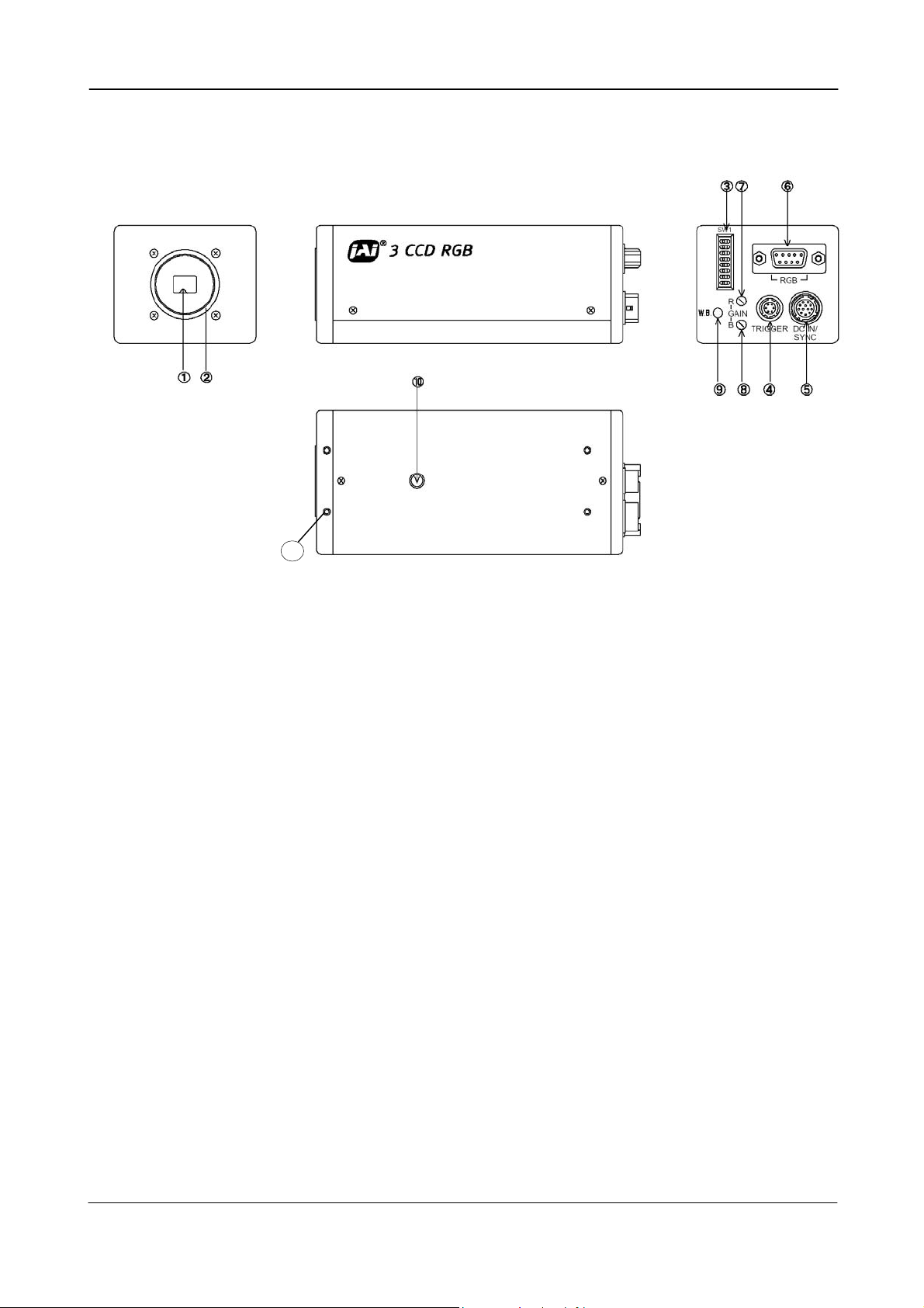
4. Locations and Functions
CV-M91
11
1. Prism
2. Lens mount (C-mount). Thread max 4 mm
3. Switch SW1 for mode settings
4. 6 pin Trigger input and RS-232C connector
5. 12 pin DC in/Sync connector
6. 9 pin Sub-D connector for video
7. Red gain potentiometer
8. Blue gain potentiometer
9. Switch for one push white balance
10. Mounting hole 1/4” for tripod. ¼ - 20
11. M3 mounting holes 4x
Fig. 1. Locations
- 3 -
Page 5
CV-M91
5. Pin Assignment
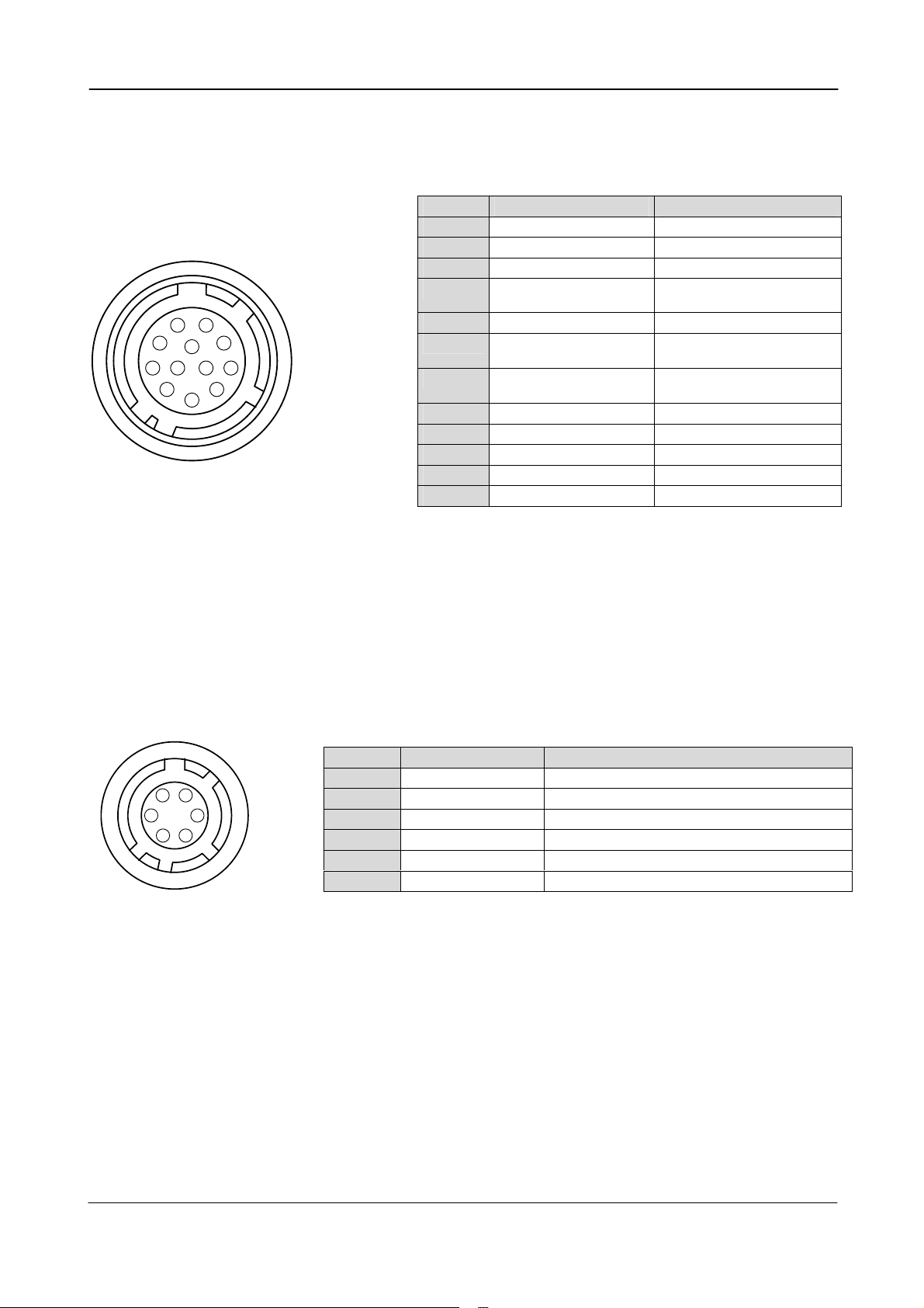
5.1. 12-pin Multi-connector (DC-IN/Trigger)
Type: HR10A-10R-12PB-01(Hirose) male.
Plugs for cable: HR10A-10P-12S
(Seen from rear of camera.)
9
1
2
11
3
4
8
10
7
12
6
5
Fig. 2. 12-pin connector.
Factory setting in bold italic.
Refer to “7. Configuring the Camera.”
Pin no. Signal Remarks
1 GND
2 +12 V DC input
3 N/C
4 NC/VBS video out
5 GND
6 HD in/HD out
7 VS in/VD in/VD out
8 GND
9 NC/Pixel clock out
10 GND
11 +12 V DC input
12 GND
Notes:
*) Alternative signal by internal switch/jumper
*), VBS 75 Ω source
SW604-1 on for VBS out
75 Ω term. By SW301-1
*), HD out 75 Ω source
75 Ω term. By SW301-2
*), VD out 75 Ω source
*), 75 Ω source
5.2. 6-pin Multi-connector (TRIGGER and RS232C)
Type: HR10A-7R-6PB (Hirose) male
Plugs for cable: HR10A-7P-6S
Seen from rear.
Pin no. Signal Remarks
1 TXD out
1
6
2
5
3
4
2 RXD in
3 GND
4 EEN output
5 Trigger input
6 WEN output
Fig. 3. 6-pin connector.
Notes:
Refer to “7. Configuring the Camera.”
EEN (Exposure Enable) pulse indicates the duration of the shutter, and can be used for
controlling strobe illumination.
EEN will be low all the time in normal continous mode if the shutter is off.
WEN (Write Enable) pulse indicates the period of effective video signal output. It is
usefull for setting the timing with framegrabber.
For schematic diagram of the input and output circuit with alternative settings refer to 5.3.
RS-232C
RS-232C
75 Ω source
75 Ω termination by int. switch SW301-3
75 Ω source
- 4 -
Page 6
CV-M91
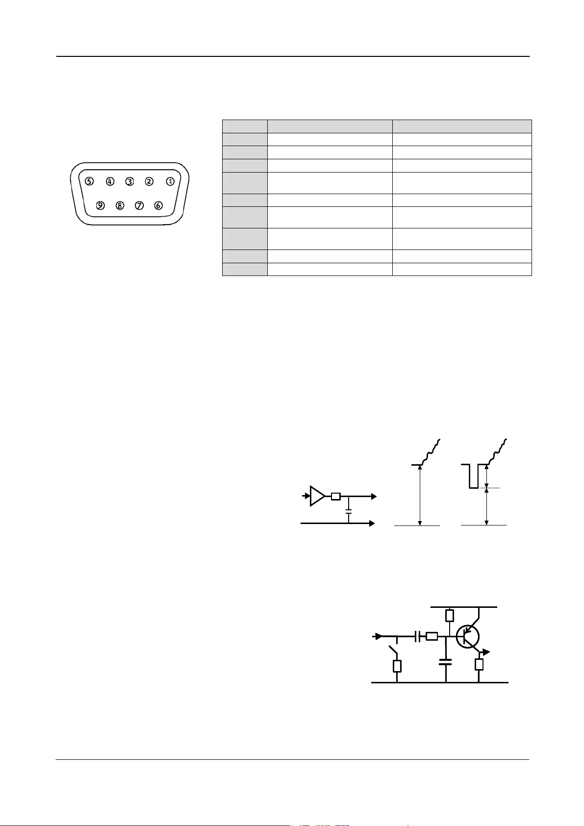
5.3. 9-pin Sub D-connector (Video)
Type: male.
(Seen from rear of camera.)
Fig. 4. 9-pin connector.
Factory setting in bold italic.
*) Alternative signals by internal switch/jumper.
Refer to “7. Configuring the Camera.”
Pin no. Signal Remarks
1 GND
2 GND
3 R output
4 G out or G+S output
5 B output
6 Y video out or VBS out
7 Sync out or WEN out
8 GND
9 C video out
N
Notes:
75 Ω source.
75 Ω source.
*) , SW604-4 off for G out
75 Ω source
75 Ω source.
*), SW604-2 off –3 on for Y out
75 Ω source
*), JP303 o JP304 c for Sync out
75 Ω source
5.4. Input and Output Circuits
In the following schematic diagrams the input and output circuits for video and timing signals
are shown.
Video outputs
The video output is a 75 Ω DC coupled circuit.
The video DC level for video and video + sync
are shown with 75 Ω termination.
Fig. 5. Video output.
HD, VD and Trigger input
The inputs are AC coupled.
Input level 4 V ±2 V.
The trigger input impedance is
high. It can be 75Ω terminated by
closing the switch.
Fig. 6. HD, VD and Trigger input.
- 5 -
VD, HD,
VD, HD,
Trigger
Trigger
75
75
75
input
input
Video
Video
Video
Output
Output
Output
GND
GND
GND
75
75
75
+5V
+5V
+5V
10u
10u
10u
800 mV
800 mV
800 mV
33k
33k
33k
1k2
1k2
1k2
47p
47p
47p
300 mV
300 mV
300 mV
500 mV
500 mV
500 mV
Page 7
CV-M91
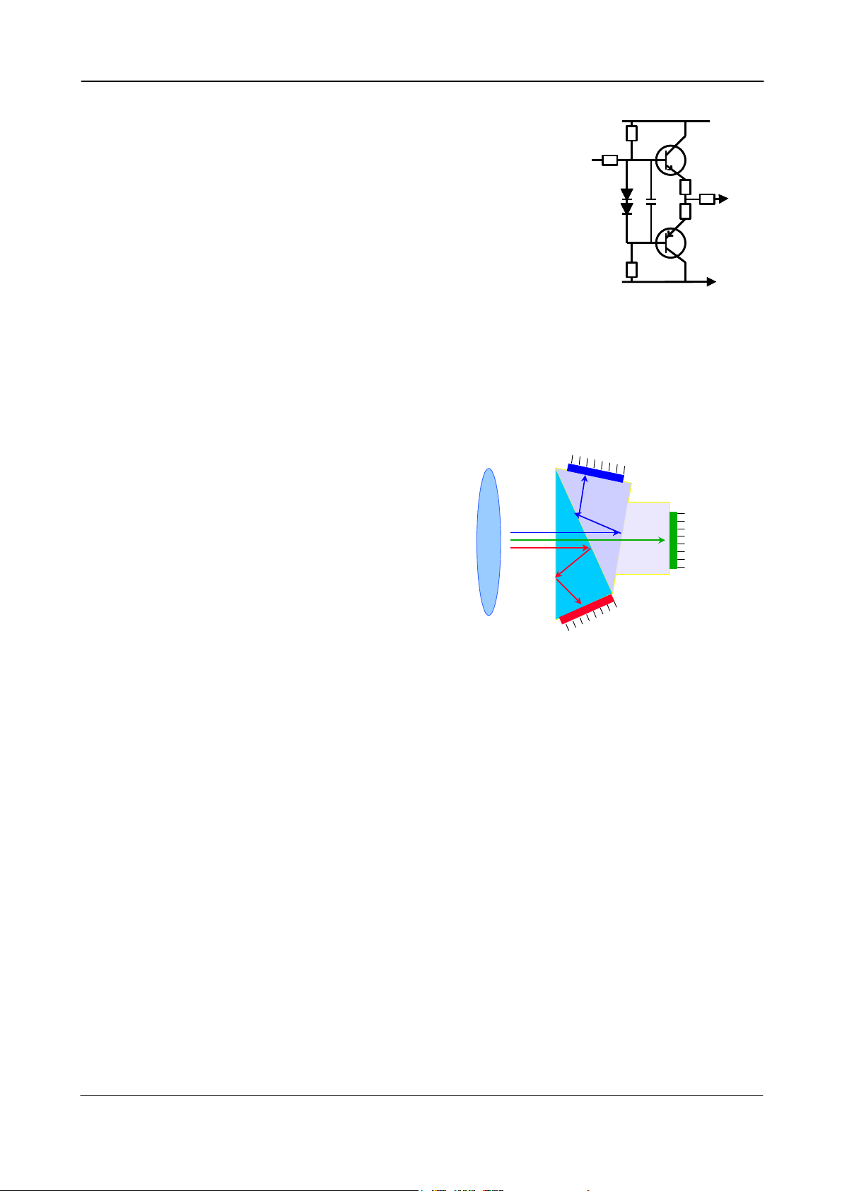
HD, VD, WEN, EEN and PCLK output
The output circuit for HD, VD, WEN, EEN and PCLK
are complementary emitter followers with 75 Ω in series.
Output level is 4V. (Non-terminated).
Fig. 7. HD and VD output.
5.5. Prism unit
For best color performance, the lens
should be designed for 1/3” 3CCD camera.
Otherwise color shading can be a problem.
Fig. 9. Principle for prism unit.
TTL
TTL
10k
10k
220
220
10k
10k
Blue CCD
Red CCD
67
10
10
10
10
Green CCD
67
GND
GND
- 6 -
Page 8
CV-M91
6. Functions and Operations
The different camera modes and functions can be set by switches and jumpers. Some functions
like RGB setup and white clip can only be changed via RS-232C.
Function names within “ “ are names used in camera control tool.
6.1. Input/Output of Signals
6.1.1. Input/output of HD/VD
In the default setting the camera will accept external HD/VD signals on pin 6 and 7 of the 12 pin
Hirose connector. If external HD/VD is applied, the camera will synchronize to it. If no external
sync signals are applied, the camera will operate with its internal x-tal controlled sync.
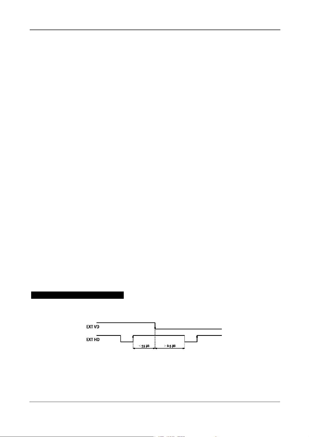
The time requirements to the relation between VD and HD are shown in fig. 10.
The input is TTL level as factory setting. It can be 75 Ohm terminated by an internal switch.
Internal HD/VD signals can be output on pin 6 and 7 by internal jumper settings. The output is
TTL level from a 75-Ohm source. In trigger modes a VD pulse will only be output after an
external trigger pulse.
Refer to “7. Configuring the Camera.”
To use this mode:
Set function on PK8407: JP305 s, JP306 o for ext. VD input. Factory default.
JP308 s, JP309 o for ext. HD input. Factory default.
SW301-1(HD), SW301-2(VD) to OFF for TTL level. Factory default.
SW301-1(HD), SW301-2(VD) to ON for 75 Ω termination
JP305 o, JP306 s for int. VD output
JP308 o, JP309 s for int. HD output
Input/output: Ext. VD in or int. VD out on pin 7 on 12-pin connector.
Ext. HD in or int. HD out on pin 6 on 12-pin connector.
If only a composite VS signal is available, it is possible to enable an internal sync separator to
separate HD and VD from the composite signal.
To use this mode:
Set jumper on PK8407: JP312 s, JP313 o, JP315 o, JP318 s, JP319 o for HD/VD input. Default.
JP312 o, JP313 s, JP315 s, JP318 o JP319 s for comp. VS input.
Input Ext. VS (1Vpp ±30%) on pin 7 on 12 pin connector.
Important notes on using this mode.
• External sync system should follow the camera scanning system
• Requirements to HD/VD phase is shown in fig. 10
Fig. 10. Ext. HD and VD phase conditions.
- 7 -
Page 9

CV-M91
6.1.2. Internal sync out/WEN out
On pin #7 on 9 pin sub-D connector, the factory setting is the internal composite sync signal out.
By jumper settings it can be changed to WEN out.
Refer to “7. Configuring the Camera.”
To use this mode:
Set function on PK8407: JP303 o, JP304 s for sync output. Factory default.
JP303 s, JP304 o for WEN output.
6.1.3. Internal pixel clock out
The internal pixel clock can be output on pin #9 on the 12 pin connector. As factory setting it is
not connected.
Refer to “7. Configuring the Camera.”
To use this mode:
Set function on PK8407: JP310 o, for no pixel clock out. Factory default.
JP310 s, for pixel clock out.
Important notes on using this mode.
• If not used, the pixel clock should not be output.
6.1.4. VBS out on pin#4 12 pin.
On pin #4 on the 12 pin connector, the video signal can be output as a composite signal.
Refer to “7. Configuring the Camera.”
To use this mode:
Set function on PK8404: SW604-1 on for VBS video signal out on pin #4 12 pin. Factory default.
SW604-1 off for no signal out on pin #4 12 pin.
6.1.5. Y out/VBS out on pin#6 9 pin sub-D.
The signal output on pin #6 on the 9 pin sub.D connector can be changed from Y output to
composite video output.
Refer to “7. Configuring the Camera.”
To use this mode:
Set function on PK8404: SW604-2 off, SW604-3 on for Y out on pin #6 9 pin. Factory default.
SW604-2 on, SW604-3 off for VBS out on pin #6 9 pin.
6.1.6. Green out/sync on green on pin#4 9 pin sub-D.
The green signal output on pin #4 9 pin sub-D can be changed to be composite sync on green.
Refer to “7. Configuring the Camera.”
To use this mode:
Set function on PK8404: SW604-4 off for green video out on pin #4 9 pin. Factory default.
SW604-4 on for sync on green out on pin #4 9 pin.
- 8 -
Page 10

CV-M91
6.2. Trigger Modes
This camera can operate in 5 primary modes. 1 non-triggered, 3 external H synchronous trigger
modes and 1 long time integration mode.
1.
Normal continuous Mode. Pre-selected exposure.
2.
Edge Pre-select Mode. Pre-selected exposure.
Pulse Width Control Mode. Pulse width controlled exposure.
3.
Start Stop Mode Exposure start on trigger, end after ext. VD
4.
5.
Long time integration Accumulation controlled by ext. VD interval
In normal continuous mode and edge pre-select mode the shutter time can be selected from the
8 fixed steps. To avoid jitter, the trigger should be synchronized to HD as shown in fig. 11.
Fig. 11. Trigger/HD timing.
Fig. 12. Horizontal timing with ext. HD sync.
756 clk NTSC
744 clk PAL
- 9 -
Page 11

CV-M91
6.2.1. Continuous Operation (Non triggered)
Trigger Mode Normal. It is for applications where the camera is continuous running without
external trigger. The shutter will work in all 8 steps up to 1/10,000 second.
Refer to “7. Configuring the Camera.”
To use this mode:
Set function: Trigger mode “Normal”. SW1-4 to OFF
On PK8407: JP301 open, JP302 open, JP331 short. Factory setting.
Accumulation to “Frame” or “Field”. SW 301-4 to ON or OFF
Scanning to “Interlaced” or “Non-Interlaced”. SW 1-5 to OFF or ON
“Shutter Speed”. SW1-1 through 1-3 to optimum
Other functions
Important notes on using this mode.
Fig. 13. PAL horizontal timing
Fig. 14. NTSC horizontal timing
- 10 -
Page 12

CV-M91
Fig. 15. Vertical timing PAL interlaced
Fig. 16. Vertical timing PAL non-interlaced. Field accumulation
- 11 -
Page 13

CV-M91
Fig. 17. Vertical timing NTSC interlaced
Fig. 18. Vertical timing NTSC non- interlaced. Field accumulation
- 12 -
Page 14

CV-M91
6.2.2. Edge Pre-select Mode
The exposure will start at the first HD after the trigger leading edge, and it stops after the
selected shutter time, and the resulting video is read out.
An EEN pulse indicate the accumulation time, and a WEN pulse that the resulting video read out.
Refer to “7. Configuring the Camera.”
To use this mode:
Set function: Trigger mode to “Edge pre-select”. SW 1-4 to ON
On PK8407: JP301 open, JP302 open, JP331 short. Factory setting.
Accumulation to “Field”. SW 301-4 to OFF
Scanning to “Non-interlaced”. SW 1-5 to ON
“Shutter Speed”. SW 1-1 through 1-3 to optimum
Other functions
Input: Ext. trigger to pin 5 on 6-pin connector.
Ext HD to pin 6 on 12 pin connector. (If used).
Important notes on using this mode.
• The duration of the trigger should be >1H. (>64µsec.)
• To avoid 1H jitter it is recommended to synchronize the trigger to HD. (See fig. 11.)
• A new trigger can not be applied before WEN is high
Fig. 19. Vertical timing for edge pre-select PAL
Fig. 20. Vertical timing for edge pre-select NTSC
- 13 -
Page 15

CV-M91
6.2.3. Pulse Width Control Mode
The exposure will start at the first HD after the trigger leading edge, and it stops between the
first and second HD after the trigger trailing edge. An EEN pulse indicate the accumulation time,
and a WEN pulse indicates that the resulting video is read out.
Refer to “7. Configuring the Camera.”
To use this mode:
Set function: Trigger mode to “Pulse width control”. SW 1-4 to ON
On PK8407: JP301 open, JP302 open, JP311 open.
Accumulation to “Field”. SW 301-4 on PK8407 to OFF
Scanning to “Non-interlaced”. SW 1-5 to ON
Shutter Speed to “1/10,000”. SW 1-1 through 1-3 to ON
Other functions
Input: Ext. trigger to pin 5 on 6-pin connector.
Ext HD to pin 6 on 12 pin connector. (If used).
Important notes on using this mode.
• The duration of the trigger can be >1H to <900H. (>64 µsec. to <60msec.)
• To avoid 1H jitter it is recommended to synchronize the trigger to HD. (See fig. 11.)
• A new trigger can not be applied before WEN is high
Fig. 21. Vertical timing for pulse width control PAL
Fig. 22. Vertical timing for pulse width control NTSC
- 14 -
Page 16

CV-M91
6.2.4. Start Stop Mode
The exposure time is controlled by the interval between the ext. trigger and the ext. VD signal.
The exposure starts at the first HD pulse after the falling edge of the ext. trigger, and stops 14.5
H after the falling edge of the VD pulse. It means that the trigger pulse must be applied after
the external VD pulse, for exposures less than 14.5 H. The range can be between 1/77 to
1/10,000. The Start/Stop mode is a continuous mode where the VD signal must be given
continuously. It is not possible to input external VD randomly.
The difference between interlaced frame and field accumulation can be explained as follow.
Both modes have 2 fields output in an interlaced frame. With frame accumulation, the contents
in the ODD and EVEN sync fields will come from sensing field 1 and 2 on the CCD sensor. With
field accumulation both ODD and EVEN sync fields will contain the signal from sensing field 1 and
2 added together. Non-interlaced field accumulation needs only 1 trigger pulse for each field.
Refer to “7. Configuring the Camera.”
To use this mode:
Set function: Trigger mode to “Start Stop”. SW 1-4 to OFF
On PK8407: JP301 short, JP302 open, JP311 short.
Accumulation to “Field” or “Frame”. SW 301-4 to OFF or ON
Scanning to “Non-interlaced” or “Interlaced”. SW 1-5 to ON or OFF
Shutter Speed to “1/10,000 ”. SW 1-1 through 1-3 to ON
Other functions
Input: Ext. trigger to pin 5 on 6-pin connector.
Ext. VD to pin 7 on 12-pin connector
(Ext. HD to pin 6 on 12-pin connector). Option
Important notes on using this mode.
• External sync system should follow the camera scanning system
• Requirements to HD/VD phase is shown in fig. 10
e x t. T rig
ext. HD
ext. VD
Accum
com po site
video
Fig. 23. Start stop interlaced field integration
Fig. 24. Start stop interlaced frame integration
Fig. 25. Start stop non-interlaced field integration
13H
accumulation
stops here
Fig. 26. Vertical timing details for start stop
- 15 -
M in. accum .
Page 17

CV-M91
6.2.5. Long time integration
The exposure time is the interval between 2 ext. VD pulses sent to the VD input. (Pin No. 7 of
the 12-pin connector). The exposure starts after input of the first ext. VD pulse, and ends after
the next input of the next ext. VD pulse, which again starts a new exposure. The long time
exposure is a continuous process where each external VD will synchronize the camera, stop the
exposure, start a new exposure and read out the previous accumulated signal. The exposure
time can be selected in intervals of complete vertical timing periods. (Interlaced frame: EIA
525H and CCIR 625H. Non-interlaced field EIA 262H and CCIR 312H).
Refer to “7. Configuring the Camera.”
To use this mode:
Set function: Trigger mode to “Long Time integrationl”. SW 1-4 to OFF
On PK8407: JP301 open, JP302 short, JP311 short.
Accumulation to “Field” or “Frame”. SW 301-4 to OFF or ON
Scanning to “Non-interlaced” or “Interlaced”. SW 1-5 to ON or OFF
Shutter Speed to “OFF ”. SW 1-1 through 1-3 to OFF
Other functions
Input: Ext. VD to pin 7 on 12-pin connector
(Ext. HD to pin 7 on 12-pin connector). Option
Important notes on using this mode.
• The exposure range is from 1 field to ∞. However it is recommended not to use exposure
over 2 seconds due visible dark current signals.
• The ext. VD signal should follow the camera sync system and interlace setting.
• Requirements to HD/VD phase is shown in fig. 10.
Fig. 27. Long time interlaced field integration
Fig. 28. Long time interlaced frame integration
Fig. 29. Long time non-interlaced field integration
- 16 -
Page 18

CV-M91
6.3. Other Functions.
Refer to “7. Configuring the Camera.”
Scanning: SW1-5 on rear selects interlaced or non-interlaced. Non-interlaced PAL = 312H in
EVEN field. Non-interlaced NTSC = 262 H in ODD field.
Gamma: SW1-6 on rear for gamma select. Gamma = 1 or gamma =0.45.
Gain: SW1-7 on rear select manual gain or AGC. Manual gain is set by VR7 on PK8406. In
AGC the gain is automatic. The AGC level is set by potentiometer VR3.
Control: SW1-8 on rear selects the camera control mode. Either local by switches, or remote
by “Camera Control Tool” via RS-232C. (Should be in position before power on.)
HD/VD in/out:
Jumper JP305 and JP306 on PK8407 are for switching between VD in/VD out.
Jumper JP308 and JP309 on PK8407 are for switching between HD in/HD out
75 Ohm termination:
SW301 on PK8407 can terminate signal inputs from TTL to 75 Ω.
SW301-1 for HD. SW301-2 for VD. SW301-3 for ext. trigger. (On for 75Ω.)
VD/VS in: Jumper JP312, JP313, JP315, JP318 and JP319 on PK8407 select ext. HD/VD in or
composite signal to the sync separator, which separate HV/VD.
Sync/WEN: Jumper JP303 and JP304 on PK8407 for Sync or WEN out on pin #7 on 9 pin sub-D.
Sync on green:
SW604 on PK8404 to ON for composite sync signal on green video output.
Pixel clock out:
Jumper JP301 on PK8407 short for pixel clock out on pin #9 on 12-pin connector.
Frame/field accumulation:
SW301-4 on PK8407 for frame or field accumulation.
CCD iris: SW201 on PK8408 to ON for CCD iris function in the regulation. The reference level
can be set by potentiometer VR10 on PK8406.
One Push White Balance:
SW202 on PK8408 switch between manual and one push white balance. Manual
allows the white balance to be set by R and B potentiometer on rear. One push is
done automatic if switch on camera rear is pressed.
Red and Blue gain setting:
R and B gain potentiometer on camera rear is for manual white adjust.
Manual gain:
VR7 on PK8406 is for manual gain setting. *)
CCD iris setting:
VR10 potentiometer on PK8406 is for CCD iris reference level. *)
AGC setting:
VR3 potentiometer on PK8406 is for AGC reference level. *)
The following functions are for RS 232C control only.
Red, Green and Blue gain level. *)
Red, Green and Blue white clip level. *)
Red, Green and Blue offset level. *)
*) Do not adjust these settings unless you are familiar with color camera adjustments.
- 17 -
Page 19

CV-M91
7. Configuring the Camera
7.1 Switch settings
The switch positions are shown in factory setting. Names in bold italic is factory setting.
7.1.1. SW1 on rear panel
SW 1 on rear
1/60
OFF
SHUTTER
TRIGGER
INTERLACE
GAMMA
GAIN
CONTROL
ON
1
2
3
4
5
6
7
8
<
<
<
Normal
Intel.
Gam. 1
Man.
Local
7.1.2. Switch settings inside
On pin #4 12P
On pin #6 9P
On pin #4. 9P
Fig. 31. Switch on PK8404 for video output.
Note:
SW1-1 through 3 OFF:
In Normal mode: The shutter is OFF
In Trigger mode: 1/50 for PAL. 1/60 for NTSC
SW1-1 through 2 OFF. SW1-3 ON:
In Normal mode: 1/100
In Trigger mode: 1/125
1/125
<
<
>
1/1000
1/250
1/500
>
<
<
<
>
>
<
>
<
< >
< > Non-interl.
< >
< >
< >
1/2000
1/4000
1/10,000
>
>
>
>
<
>
>
>
<
Random
Gam. 0.45
AGC
RS-232C
second
.
Fig. 30. Mode switch on camera rear
SW 604 on PK 8404
ON
VBS out
Y/VBS out
Sync on G
1
2
3
4
OFF
VBS
< >
> <
< >
G+S < > G
NC
Y - VBS
SW 301 on PK 8407
HD term.
OFF
VD term.
Trig term.
Accumul.
ON
1
2
3
4
TTL
TTL
TTL
field
< >
< >
< >
< >
75 Ohm
75 Ohm
75 Ohm
frame
Fig. 32. Switch on PK8407 for 75Ω termination and accumulation.
SW 201 on PK 8408
OFF
CCD iris
ON
1
Off
< >
CCD iris on
Fig. 33. Switch on PK8408 for CCD iris.
SW 202 on PK 8408
OFF
White bal.
ON
1
Man.
< >
One push
Fig. 34. Switch on PK8404 for white balance.
- 18 -
Page 20

CV-M91
7.2. Jumper settings inside
Factory settings is shown in bold italic
HD/VD input output on pin #6 and #7 on 12 pin connector.
Jumper HD/VD in HD/VD out Remarks
JP305 short open
JP306 open short
JP308 short open
JP309 open short
HD/VD input on pin #6 and #7 or composite VS signal in on pin #7.
Jumper HD/VD in VS in Remarks
JP312 short open
JP313 open short
JP315 open short
JP318 short open
JP319 open short
Sync out/WEN out on pin #7 on 9 pin sub-D connector.
Jumper Sync out WEN out Remarks
JP303 open short
JP304 short open
Pixel clock out on pin #9 on 12 pin on 12 pin connector.
Jumper N. C. Pix clk out Remarks
JP310 Open short
Mode setting by internal jumpers
Jumper Normal Edge pre-s Pulse width Start/stop Long time Remarks
JP311 short open short short
JP301 open open short open
JP302 open open open short
VD input/output.
HD input/output.
Instead of HD and VD input on pin #6 and pin #7 a composite signal VS can
be input on pin #7. The internal sync separator will then separate HD and
VD.
Keep JP310 open if pixel clock is not used.
- 19 -
Page 21

r
7.3. Switch and jumper positions
Front
1
Fig. 35. Board positions.
SW 604
SW 604 for
Video output
Fig. 37. Switches on PK8404. Fig. 38. Switches on PK8408.
VR 7
JP310 JP311 JP315 JP318 JP319 JP302 JP309 JP305
Fig. 36. Jumpers and switches on PK8407.
Fig. 39. Potentiometers on PK8406.
CV-M91
4
3
JP 312JP 301 JP 313 JP 304 JP 303 JP 308
SW 201
Off <-> ON
VR 10
- 20 -
VR 3
Rear
2
JP 306
SW 301
1. PK8407
2. PK8404
3. PK8406
4. PK8408
SW 301 for
75Ω term.
SW 202
Off <-> ON
VR 3 = AGC
VR 7 = Manual gain
VR 10 = CCD iris
SW 201 fo
CCD iris
SW 202 for
White bal.
Page 22

CV-M91
7.3. RS-232C control
The CV-M91 camera functions can be set up via the RS-232C port on the 6 pin HR connector. The
JAI camera control tool for CV-M91 can be used for it.
To use this mode:
Set function: Control. SW1-8 on rear to ON. RS-232C. (Switch setting before power on).
Other functions
Important notes on using this mode.
•
Communication setting.
1 CD
Baud Rate 9600 bps
Data Length
8 bit
Start Bit 1 bit
Stop Bit 1 bit
Parity None
Xon/Xoff Control None
RS 232C cable
CAMERA
CAMERA
TXD
TXD
RXD
RXD
GND
GND
1 CD
4 DTR
4 DTR
6 DSR
6 DSR
2 RXD
2 RXD
3 TXD
3 TXD
5 GND
5 GND
7 RTS
7 RTS
8 CTS
8 CTS
9 CI
9 CI
9 pin
9 pin
D-con
D-con
PC COM
PC COM
PORT
PORT
7.4. CV-M91command list
The following functions can be controlled via the camera control tool.
Shutter speed
1/60 to 1/10,000 sec.
Mode
Normal, random trigger
Scanning
2.1 interlaced, non-interlaced
Accumulation
Frame, field
Gamma
Gamma 1.0, gamma 0,45
AGC
AGC off, AGC on, manual gain, AGC reference level
CCD iris
CCD iris on. CCD iris off, CCD iris reference level
White balance
One push, manual, red gain, blue gain, green gain
White clip level
Red white clip, blue white clip, green white clip
Offset level
Red offset, blue offset, green offset
Load user settings
Load factory, user 1, user 2
Save user settings
Save user 1, save user 2. (Last saved user settings become default at next power-up.)
- 21 -
Page 23

CV-M91
7.5. Camera Control Tool for CV-M91
From www.jai.com Camera Control Tool for Windows 98/NT/2000 can be downloaded.
The control tool contains a camera control program and tools for making your own program.
For the integrator and experienced user, the Camera Control Tool is much more than a program
with a window interface. It also provides an easy and efficient ActiveX interface built for MS
Windows 98, ME, NT and 2000. The OCX interface has the ability to connect to the camera using
the serial interface of the PC by reading and writing properties for the camera. This integration
requires simple programming skills within Visual Basic, Visual C++ or similar languages in a
Microsoft Windows environment.
Below the different windows are shown.
Fig. 40. Window from camera control tool
- 22 -
Page 24

CV-M91
8. External Appearance and Dimensions
Important notes.
• C-mount thread on lens should be less than 4.0 mm.
• Use only lenses designed for 1/3” 3 CCD cameras.
Fig. 41. Outline.
9. Specifications
9.1. Spectral sensitivity
The resulting relative response for the prism and the CCD sensor characteristics combined.
1.0
1.0
0.8
0.8
G R
G R
0.6
0.6
0.4
0.4
B
B
0.2
0.2
Relative response
Relative response
0.0
0.0
400 500 600 700 800
400 500 600 700 800
Wave length (nm)
Wave length (nm)
Fig. 42. Spectral sensitivity for CV-M91
- 23 -
Page 25

CV-M91
9.2. Specification table
Specifications CV-M91P CV-M91N
Scanning system
Frame rate 50 Hz 59.94 Hz
Line frequency 15.625 kHz 15.734 kHz
Pixel frequency 14.25 MHz 14.349949 MHz
CCD sensors 3 x 1/3” monochrome IT CCD
Sensing area 4.8 (h) x 3.6 (v) mm
Effective pixels 752 (h) x 582 (v) 768 (h) x 494 (v)
Pixels in video output 744 (h) x 575 (v) 765 (h) x 486 (v)
Cell size
Resolution horizontal 570 TV lines
Sensitivity (on sensor) 0.5 Lux, Max gain, 50% video
S/N ratio 54 dB 56 dB
Video outputs. (DC coupled) RGB
Video output level
Gamma 1.0 - 0.45
Gain
Gain range
Accumulation Field – Frame
Synchronization Int. X-tal. Ext HD/VD or random trigger
Scanning 2:1 interlaced, non-interlaced
Composite VS input
Composite sync output
HD/VD sync input
HD/VD sync output
Trigger input
WEN output (write enable)
EEN output (exposure enable)
Pixel clock output
Shutter.
Continuous and Edge pre-select
Pulse width control input 1 H to 900 H
Start/stop 1/10,000 to 1/77 second
Long time exposure
White balance Manual, one push (2350 to 6400 K)
Functions controlled by
RS 232C
Functions controlled by internal DIP
switches
Operating temperature
Humidity 20 - 80% non-condensing
Storage temp./humidity
Vibration 3 G (15 Hz – 200 Hz in XYZ)
Shock 50 G
Regulations CE (EN 50081-1, EN 50082-1) FCC part 15
Power
Lens mount C-mount. (Max 4.0 mm thread)
Dimensions 50 x 60 x 130 mm (HxWxD)
Weight 480 g
CCIR PAL, 25 frames/sec.
625 lines, 2:1 Interlaced
ICX-409AL-6
6.5 (h) x 6.25 (v) µm 6.35 (h) x 7.4 (v) µm
Y/C PAL
VBS PAL
RGB and C signal, 0.7 Vpp, 75 Ω
G on sync, Y signal and Composite VS, 1.0 Vpp, 75 Ω
Manual – Automatic
0 to +18 dB
1.0 Vpp ±0.3V. 75 Ω terminated
4 Vpp from 75 Ω source
4 Vpp ±2 V. (Termination TTL or 75 Ω)
4 Vpp from 75 Ω source
4 Vpp ±2 V. (Termination TTL or 75 Ω)
4 Vpp from 75 Ω source
4 Vpp from 75 Ω source
4 Vpp from 75 Ω source
(off), 1/100, 1/250, 1/500, 1/1000, 1/2000, 1/4000, 1/10,000 sec.
1 field to ∞
Trigger mode, Shutter speed, Accumulation, Interlace, AGC level, White clip,
Set-up, Manual gain, AGC/manual gain, Internal/ potentiometer gain set,
Gamma, white balance.
VD input/output, HD input/output
HD, VD and Trigger 75 Ω termination on/off
-5°C to +45°C.
-25°C to 60°C./20% - 90 % non-condensing
12V DC ± 10%. 6 W
EIA NTSC. 30 frames/sec.
525 lines, 2:1 Interlaced
3 x 1/3” monochrome IT CCD
ICX-408AL-6
RGB
Y/C NTSC
VBS NTSC
- 24 -
Page 26
CV-M91
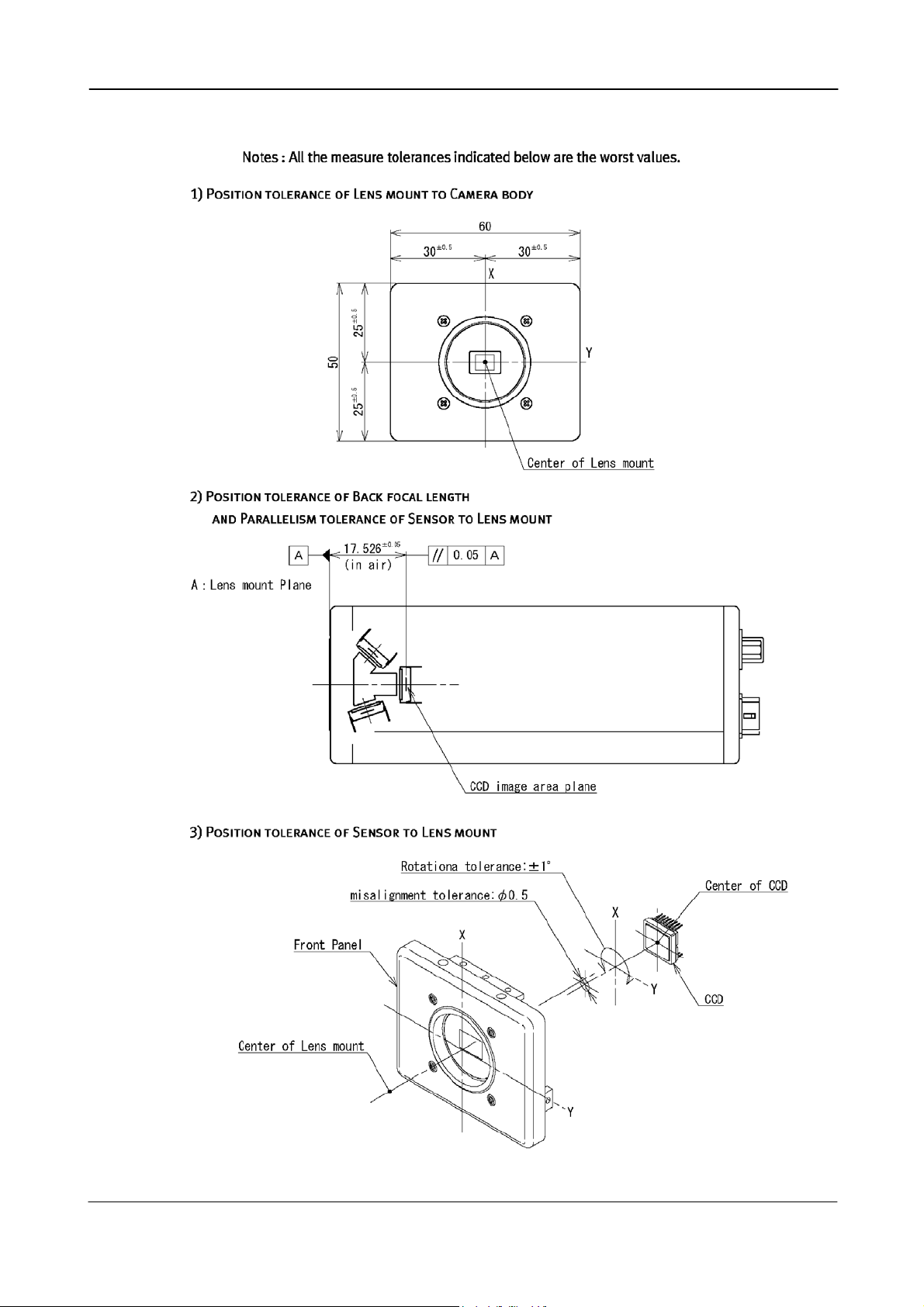
9.3. CV-M91 Opto-mechanical specifications
Fig. 43. Opto mechanical specifications.
- 25 -
Page 27

CV-M91
10. Appendix
10.1. Precautions
Personnel not trained in dealing with similar electronic devices should not service this camera.
The camera contains components sensitive to electrostatic discharge. The handling of these
devices should follow the requirements of electrostatic sensitive components.
Do not attempt to disassemble this camera.
Do not expose this camera to rain or moisture.
Do not face this camera towards the sun, extreme bright light or light reflecting objects.
When this camera is not in use, put the supplied lens cap on the lens mount.
Handle this camera with the maximum care.
Operate this camera only from the type of power source indicated on the camera.
Power off the camera during any modification such as changes of jumper and switch setting.
10.2. Typical CCD Characteristics
The following effects may be observed on the video monitor screen. They do not indicate any
fault of the CCD camera, but do associate with typical CCD characteristics.
V. Smear
Due to an excessive bright object such as electric lighting, sun or strong reflection, vertical
smear may be visible on the video monitor screen. This phenomenon is related to the
characteristics of the Interline Transfer System employed in the CCD.
V. Aliasing
When the CCD camera captures stripes, straight lines or similar sharp patterns, jagged image on
the monitor may appear.
Blemishes
Some pixel defects can occur, but this does not have en effect on the practical operation.
Patterned Noise
When the CCD camera captures a dark object at high temperature or is used for long time
integration, fixed pattern noise (shown as white dots) may appear on the video monitor screen.
CV
- 26 -
Page 28

11. Users Record
CV-M91
Camera type: CV-M91
Revision: (Revision A)
Serial No. ……………..
For camera revision history, please contact your local JAI distributor.
Users Mode Settings.
Users Modifications.
DECLARATION OF CONFORMITY
AS DEFINED BY THE COUNCIL DIRECTIVE
89/336/EEC
EMC (ELECTROMAGNETIC COMPABILITY)
WE HEREWITH DECLARE THAT THIS PRODUCT
COMPLIES WITH THE FOLOWING PROVISIONS APPLYING TO IT.
EN-50081-1
Company and product names mentioned in this manual are trademarks or registered trademarks of their respective owners.
JAI A-S cannot be held responsible for any technical or typographical errors and reserves the right to make changes to products and
documentation without prior notification.
JAI A-S, Denmark
Phone +45 4457 8888
Fax +45 4491 8880
www.jai.com
JAI Corporation, Japan
Phone +81 45 440 0154
Fax +81 45 440 0166
www.jai-corp.co.jp
JAI UK Ltd, England
Phone +44 0 1895 821 481
Fax +44 0 1895 824 433
www.jai.com
JAI Pulnix Inc, USA
Phone (Toll-Free) +1 877 4445 5444
Phone +1 408 747 0300
Fax +1 408 747 0880
www.jaipulnix.com
- 27 -
EN-50082-1
 Loading...