

Page 1

Remote Head Monochrome CCD Camera
CV-M536/538/539
Operation Manual
(Rev.E)
Page 2

CV-M536/538/539
DECLARATION OF CONFORMITY
AS DEFINED BY THE COUNCIL DIRECTIVE
89/336/EEC
EMC (ELECTROMAGNETIC COMPATIBILITY)
WE HEREWITH DECLARE THAT THIS PRODUCT
COMPLIES WITH THE FOLLO WING PROVISIONS APPLYING T O IT .
EN-50081-1
EN-50082-1
Page 3

CV-M536/538/539
Table of Contents
Table of Contents ....................................................................................................................................... 2
1. General................................................................................................................................................ 3
2. Standard Composition......................................................................................................................... 3
3. Main Features ..................................................................................................................................... 4
4. Locations and Functions ..................................................................................................................... 5
4.1. CCU ............................................................................................................................................ 5
4.2. HEAD.......................................................................................................................................... 5
5. Pin Assignment ................................................................................................................................... 6
5.1. 12-pin Multi-connector (DC-IN/SYNC.) ...................................................................................... 6
5.2. 6-pin Multi-connector (TRIGGER) .............................................................................................. 6
6. Functions and Operations ................................................................................................................... 7
6.1. Input/Output of HD/VD Signal................................................................................................... 7
6.1.1. Input of External HD/VD Signal ..................................................................................... 7
6.1.2. Output of Internal HD/VD Signal ................................................................................... 7
6.2. Normal Shutter Mode ................................................................................................................ 7
6.3. External Trigger Mode ............................................................................................................... 7
6.3.1. Edge Pre-select Mode ................................................................................................... 7
6.3.2. Pulse Width Control Mode............................................................................................. 9
6.3.3. Start/Stop Trigger Mode .............................................................................................. 11
6.3.4. Long Time Exposure Mode ...........................................................................................13
7. Mode Setting......................................................................................................................................15
7.1.1. SW1 Switch on the Rear Panel......................................................................................15
7.1.2. Table for SW 1 Setting...................................................................................................15
7.1.3. Table for Shutter Time ..................................................................................................15
7.1.4. Ext. Trigger Shutter Mode.............................................................................................16
7.1.5. Trigger Select ...............................................................................................................16
7.1.6. CD Accumulation ..........................................................................................................16
7.1.7. Scanning System..........................................................................................................16
7.1.8. Gamma Correction ....................................................................................................... 16
7.1.9. Gain Control .................................................................................................................16
7.2. SW2 on PK8057 Board ..............................................................................................................16
7.3. Jumper Settings ........................................................................................................................17
7.3.1. Jumper on PK8054 Board..............................................................................................17
7.3.2. Jumper on PK8057 Board..............................................................................................17
7.3.3. Pixel Clock Output........................................................................................................17
7.4. Location of SW2 and Jumpers ...................................................................................................18
7.4.1. Board PK8054 Side B....................................................................................................18
7.4.2. Board PK8057 Side A.................................................................................................... 18
8. Adjustment of Video Signal Output Level ..........................................................................................19
9. External Appearance......................................................................................................................... 20
9.1. CCU .......................................................................................................................................... 20
9.2. HEAD........................................................................................................................................ 20
10. Specifications.....................................................................................................................................21
10.1. Spectral Sensitivity ................................................................................................................... 21
11. Appendix ........................................................................................................................................... 22
11.1. Precautions ............................................................................................................................. 22
11.2. Typical CCD Characteristics ..................................................................................................... 22
12. User’s Record .................................................................................................................................... 23
- 2 -
Page 4

CV-M536/538/539
1. General
The model CV-M536 series is a new remote micro-head camera system featuring virtually identical
performance and function of the popular CV-M50 standard machine vision camera.
Precisely installed CCD imager (1/2") and miniature size (ø17mm) allows access to very contained
spaces. The remote micro-head weights only 15g (0.031lbs) and can be separated up to 10m (32.8 feet)
by cable.
The new 1/2" Hyper HAD imager employed in the CV-M536 series provides superior sensitivity and
higher dynamic range with improved smear level.
High speed shutter and asynchronous random trigger functions allow a superb image quality in
machine vision and image processing applications such as dynamic motion image capturing, on-line
inspection, gauging, printing and graphics.
CV-M536 series offers 3-type of model with different cable length, as described in the following list.
Model Cable length
CV-M536 2.0m (6.45 feet) (Cable is directly mounted on camera head)
CV-M538 5.0m (16.40 feet) (Cable is detachable from camera head by connector)
CV-M539 10.0m (32.80 feet)(Cable is detachable from camera head by connector)
Important Notice!
CV-M536 series has inter-changeability between camera head and CCU’s within the same model.
(e.g. CV-M536 camera head
However, CV-M536 camera head
can be usedcan be used
can be used
can be usedcan be used
cannot be usedcannot be used
cannot be used
cannot be usedcannot be used
with CCU’s from other set of CV-M536’s.
with CCU’s from CV-M538/539.)
2. Standard Composition
1) Camera head x1 (incl. camera cable)
2) Camera control unit x1
3) Operation manual x1
Options (Following optional accessories are available upon request.)
1) 12pin Multi Connector (HR10A-10P-12S)
2) 6pin Multi Connector (HR10A-7P-6S)
3) MP-40 Tripod mount adaptor
4) MP-30 Micro-head fixing mount adaptor
5) MP-20 C-mount adaptor
6) OP-735 Special lens (7.5mm, F1.6)
- 3 -
Page 5

CV-M536/538/539
3. Main Features
• Miniature-sized remote head - ø17mm (0.67")
• 1/2" Hyper HAD interline transfer CCD imager, 768(H) x 494(V) for EIA and 752(H) x 582(V) for CCIR
• High resolution - horizontal 570 TV lines for EIA, 560 TV lines for CCIR
• Excellent S/N - better than 56dB
• High sensitivity - 0.05 lx minimum illumination on CCD imager
• Improved low smear and higher dynamic range
• Edge pre-select and pulse width external trigger modes
• High speed and random trigger shutter up to 1/10,000 sec.
• Long-time exposure mode - 1/30 sec. ~∞ (EIA)
- 1/25 sec. ~∞ (CCIR)
• WEN and EEN output (pixel clock output : user option) - to support further advanced image capturing
• Internal, external HD/VD synchronization
• Easy access for mode-setting of shutter and other function from rear panel
• Lens mount - Special mount type
• Durable camera cable for industrial environment - available from 2m (6.56 feet) up to 10m (32.8 feet)
- 4 -
Page 6
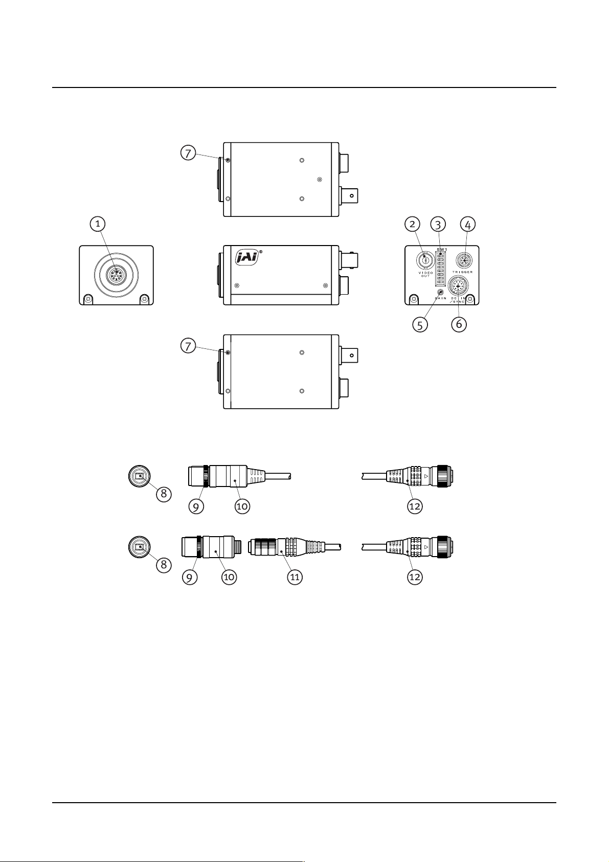
4. Locations and Functions
4-1. CCU
7
CV-M536/538/539
1
4-2. HEAD
a)CV-M536
2 3 4
5 6
7
8
9 10 12
b) CV-M538/539
8
9 10 11
1 12P connector : To connect camera head with camera control unit
(For Camera Head)
2 Video output connector : To output video VS1.0Vp-p
(BNC connector)
3 SW1 switch : To set shutter speed and function modes
4 6-pin Multi connector : Output WEN/EEN signal and input external trigger pulse, etc.
5 GAIN : To adjust gain level
6 12P Multi connector : Input DC+12V power and input/output of HD/VD signal, etc.
7 Screw holes for Tripod mount plate : To fix tripod mount plate (optional) on camera
8 CCD sensor : 1/2" Hyper HAD Interline transfer CCD sensor
9 Focus adjustment ring : To adjust lens focus
10 Camera head
11 Camera head connector : To connect camera head with cable (Only for CV-M538/539)
12 12P connector : To connect camera head with camera control unit
(For Camera Head)
12
- 5 -
Page 7
CV-M536/538/539
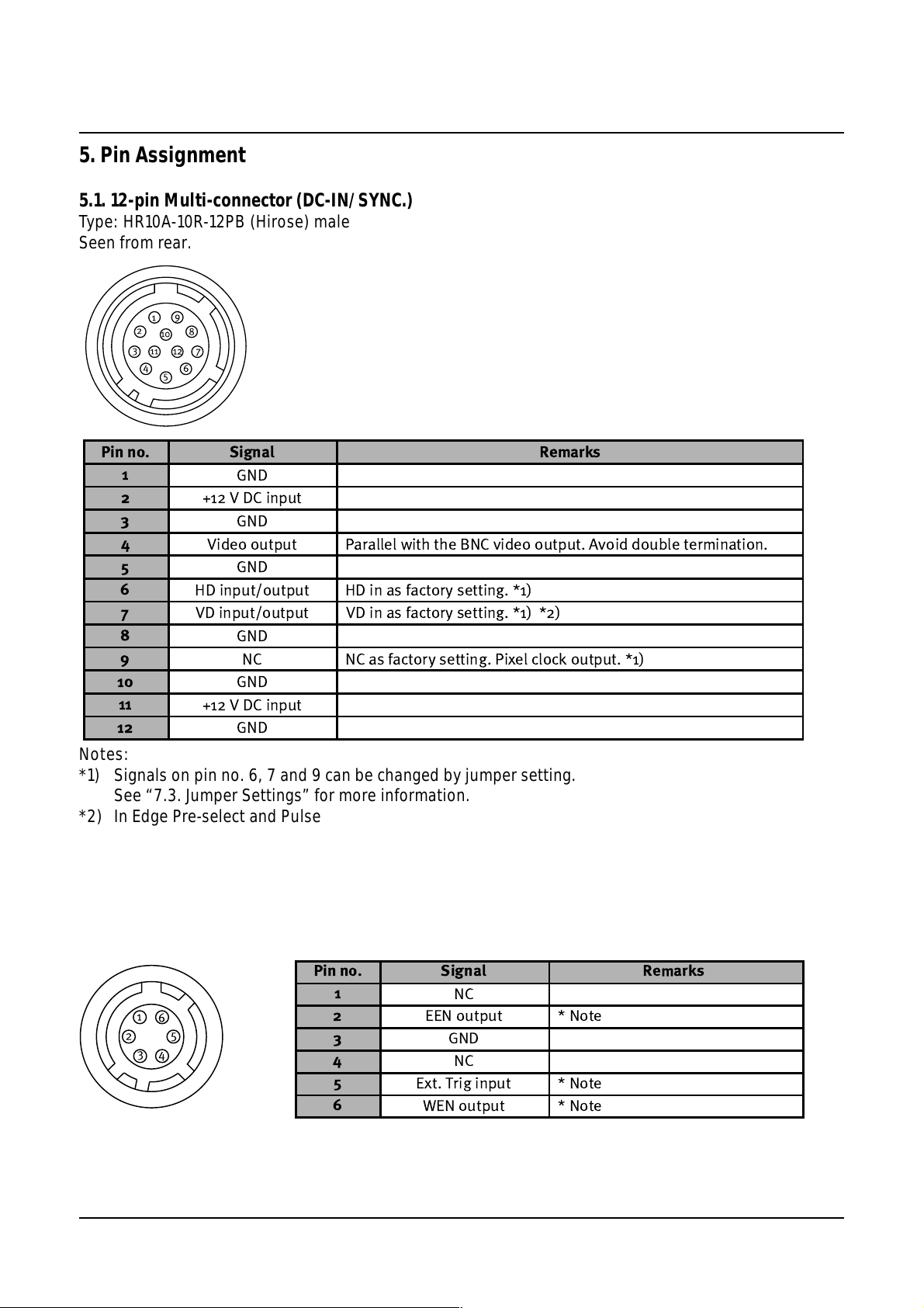
5. Pin Assignment
5.1. 12-pin Multi-connector (DC-IN/SYNC.)
Type: HR10A-10R-12PB (Hirose) male
Seen from rear.
Pin no. Signal Remarks
1
2
3
4
5
6
7
8
9
10
11
12
GND
+12 V DC input
GND
Video output Parallel with the BNC video output. Avoid double termination.
GND
HD input/output HD in as factory setting. *1)
VD input/output VD in as factory setting. *1) *2)
GND
NC NC as factory setting. Pixel clock output. *1)
GND
+12 V DC input
GND
Notes:
*1) Signals on pin no. 6, 7 and 9 can be changed by jumper setting.
See “7.3. Jumper Settings” for more information.
*2) In Edge Pre-select and Pulse Width Control mode do not input ext. VD signal.
5.2. 6-pin Multi-connector (TRIGGER)
Type: HR10A-7R-6PB (Hirose) male
Seen from rear.
Pin no. Signal Remarks
1
2
3
4
5
6
* Notes:
The functions available on the 6-pin multi-connector are not effective in
long time exposure mode.
NC
EEN output * Note
GND
NC
Ext. Trig input * Note
WEN output * Note
- 6 -
Page 8

CV-M536/538/539
6. Functions and Operations
6.1. Input/Output of HD/VD Signal
6.1.1. Input of External HD/VD Signal
As factory setting the camera can be synchronized by external HD/VD signals. The signal level must be
4.0V p-p +/- 2.0V at the input with the 75 Ohm termination ON. To change to non-terminated input, see
instructions in “7. Mode Setting”.
If no ext. HD is connected, the camera will switch to the internal X-tal controlled HD.
If no ext. VD is connected, the camera will continue with its internal VD.
6.1.2. Output of Internal HD/VD Signal
The internal HD/VD output is 4.0V p-p from a 75 Ohm source.
To select this mode, see instructions in “7. Mode Setting”.
6.2. Normal Shutter Mode
When trigger select SW1-4 is OFF, the camera is in normal mode. The SW1-1, SW1-2 and SW1-3 are for
selecting the shutter speed. The range is from OFF to 1/10,000 second in 8 steps. The camera is running
continuously with an exposure as the selected shutter time.
The shutter time setting is shown in “7.1.3. Table for Shutter Time”.
6.3. External Trigger Mode
External trigger mode of CV-M536/538/539 allows 4 different driving modes, as follow.
1 Edge pre-select mode. (Asynchronous reset and exposure start by an ext. trigger)
2 Pulse width control mode. (Exposure control by the low period of the ext. trigger)
3 Start/Stop trigger mode. (Exposure start by the ext. trigger and end by the ext. VD signal)
4 Long time exposure mode. (Exposure control by the interval of the ext. VD signal)
The trigger input is AC coupled, so there is a maximum pulse width for the trigger pulse about 60 msec.
The signal level must be 4.0V p-p +/- 2.0V on the input with the 75 Ohm termination ON. To change to
non-terminated input, see instructions in “7. Mode Setting”.
The following describes the details of each trigger mode.
6.3.1. Edge Pre-select Mode
The edge pre-select mode operation will only work in non-interlaced and field accumulation mode. The
CV-M50 starts the exposure (= accumulation of photoelectric charge) at the first HD pulse after the
falling edge of the ext. trigger pulse. The exposure ends after the time set by the 3 shutter switches
SW1-1 to SW1-3. The range is 8 steps from OFF (1/60 or 1/50) to 1/10,000 second.
In this mode, the EEN (Exposure ENable) pulse and WEN (Write ENable) pulses are generated and
output from the camera. The EEN pulse indicates the exposure time and can be used to control the
illumination such as strobe light. The EEN pulse is output from pin 2 of the 6-pin multi connector. The
signal level is 4.0 Vp-p from a 75 Ohm source.
The WEN pulse indicates the time period of the effective video signal output, and is useful for the timing
and interfacing of external devices such as frame grabbers. The WEN pulse is output from pin 6 of the 6pin multi connector. The signal level is 4.0 Vp-p from a 75 Ohm source.
The video must be read out before a new trigger can be applied. The interval between trigger pulses
must be longer than the time for 1 field + the shutter time. It is the limit for the field rate.
- 7 -
Page 9

CV-M536/538/539
To use this mode
Set: SW1-4 to ON for ext. trigger shutter
SW1-5 to OFF for field accumulation
SW1-6 to ON for non-interlaced
SW1-1,2 and 3 to shutter speed
Input: Ext. trigger to pin 5 on 6 pin multi connector.
Ext. HD to pin 6 on 12-pin multi connector. (If used).
75 Ohm termination is done with SW2-1 (HD) and SW2-2 (etc.trigger) on PK8057 board.
Refer to Timing Chart and Cautions below.
Detailed switch and jumper setting is described in “7. Mode Setting”.
For connections see “5. Pin Assignment”.
Cautions in the Edge Pre-select Mode.
1. Edge pre-select mode is effective only in non-interlaced, field accumulation mode.
2. The exposure start may delay up to 1H max., when the falling edge of ext. trigger pulse is not
synchronized with the falling edge of ext. HD signal. To avoid this 1H delay and jitter, the falling edge
of the trigger pulse should be synchronized with the HD pulse as shown below. It can be the ext. HD
input or the Internal HD output.
3. The ext. trigger input is 75 Ohm terminated as factory setting. (R127 short and SW2-2 ON). The
voltage level of the ext. trigger has to be 4.0 Vp-p ± 2.0 V. The duration should be more than 1 H
negative going. >64 µsec. and < 60 msec. The input is AC coupled.
4. If the ext. trigger input and ext. HD input are from a source with TTL level, set SW2-1 and SW2-2 OFF
for non-terminated. SW2-1 for HD signal, SW2-2 for ext. trigger pulse. See “7.2 SW2 on PK8057
Board”.
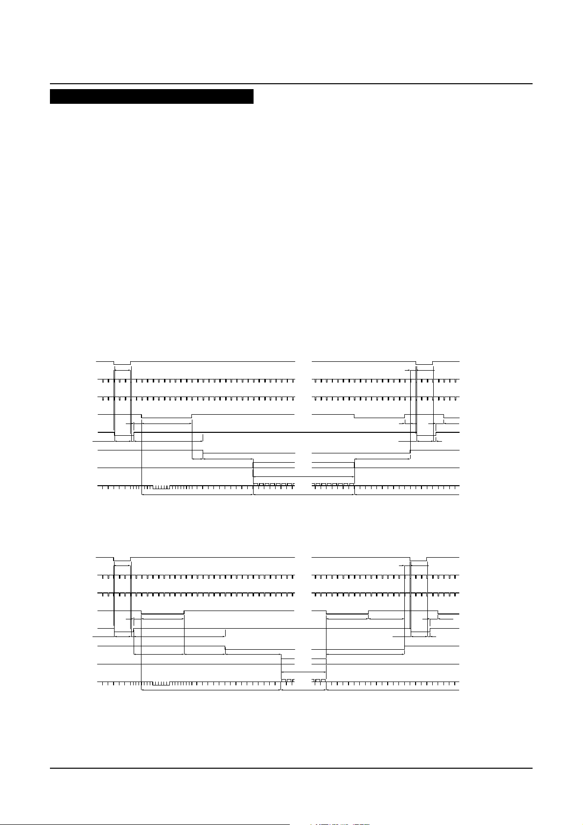
EIA (Non-interlaced / Field accumulation mode)
Edge pre-select mode (for non-interlace only
TRIG
EXT HD
INT HD
INT VD
EEN
Exposure time Exposure time
WEN
CCD out
Video out
1H more
1.5H 9H
0.5H
12.5H
10.5H
)
2H 9H
Effective pixels
No.10 to 251
20H 242H 20H
Effective videoBlanking Blanking
EIA : 1H = 63.5µs
TRIG in1H
9H1.5H1H9H
0.5H
- 8 -
Page 10

CV-M536/538/539
CCIR (Non-interlaced / Field accumulation mode)
Edge pre-select mode (for non-interlace only
TRIG
EXT HD
INT HD
INT VD
EEN
Exposure time Exposure time
WEN
CCD out
Video out
1H more
1.5H 7.5H
0.5H
16.5H
9H 10H 14H
)
7.5H
7.5H
Effective pixels
No.10 to 251
25H 287H 25H
Effective videoBlanking Blanking
CCIR : 1H = 64µs
TRIG in1H
7.5H1.5H6.5H
0.5H
6.3.2. Pulse Width Control Mode
The pulse width control mode will only work in non-interlaced field accumulation mode.
The exposure is controlled by the low period of the ext. trigger pulse. The exposure starts at the first HD
pulse after the falling edge of the ext. trigger pulse. The exposure ends at the first HD pulse after the
rising edge of the ext. trigger. The Shutter can be controlled to be within the range from >1H (>64 µsec.)
to <60 msec. The AC coupling causes the upper limit.
EEN (Exposure ENable) pulse and WEN (Write ENable) pulses are generated and output from the
camera.
The EEN pulse indicates the exposure time. The EEN pulse is output from pin 2 of the 6-pin multi
connector. The signal level is 4.0 Vp-p from a 75 Ohm source.
The WEN pulse indicates the time period of the effective video signal output and is useful for the timing
and interfacing of external devices such as frame grabbers. The WEN pulse is output from pin 6 of the 6pin multi connector. The signal level is 4.0 Vp-p from a 75 Ohm source
The video must be read out before a new trigger can be applied. The interval between trigger pulses
must be longer than the time for 1 field + the shutter time. It is the limit for the field rate.
To use this mode
Set: SW1-1, 2 and 3 to OFF
SW1-4 to ON for ext. trigger shutter
SW1-5 to OFF for field accumulation
SW1-6 to ON for non-interlaced
JP12 on PK8057 to OPEN
Input: Ext. trigger to pin 5 on 6-pin multi connector.
Ext. HD to pin 6 on 12-pin multi connector. (If used).
75 Ohm termination is done with SW2-1 (HD) and SW2-2 (ext.trigger) on PK8057 board.
Refer to Timing Chart and Cautions on next page.
Detailed switch and jumper setting is described in “7. Mode Setting”.
For connections see “5. Pin Assignment”.
- 9 -
Page 11
CV-M536/538/539
Cautions in the Pulse Width Control Mode.
1. Pulse width control mode is effective only in non-interlaced field accumulation mode.
2. The exposure start may be delayed up to 1H max., when the falling edge of ext. trigger pulse is not
synchronized with the falling edge of ext. HD signal. To avoid this 1H jitter and delay, the falling edge
of the ext. trigger pulse should be synchronized within 4.4 µsec. to the HD pulse. It can be the ext. HD
in or the Internal HD out.
See cautions in Edge Pre-select Mode page 7.
3. The ext. trigger input is 75 Ohm terminated as factory setting. (R127 short and SW2-2 on). The
voltage level of the ext. trigger has to be 4.0 Vp-p ± 2.0 V. The duration should be more than 1 H
negative going. >64 µsec. and < 60 msec. The input is AC coupled.
4. If the ext. trigger input and ext. HD input are from a source with TTL level, set SW2-1 and SW2-2 OFF
for non-terminated. SW2-1 for HD signal, SW2-2 for ext. trigger pulse. See “7.2 SW2 on PK8057
Board”.
EIA (Non-interlaced / Field accumulation mode)
Pulse width control mode (for non-interlace only
TRIG
EXT HD
1H more
)
EIA : 1H = 63.5µs
TRIG in1H
INT HD
INT VD
EEN
Exposure time Exposure time
WEN
CCD out
Video out
1.5H 9H
0.5H
12.5H
2H 9H 10H
Effective pixels
No.10 to 251
20H 242H 20H
Effective videoBlanking Blanking
CCIR (Non-interlaced / Field accumulation mode)
Pulse width control mode (for non-interlace only
TRIG
EXT HD
INT HD
INT VD
EEN
WEN
CCD out
Video out
1H more
1.5H 7.5H
Exposure time Exposure time
0.5H
16.5H
9H 10H 14H
)
7.5H
7.5H
Effective pixels
No.10 to 251
25H 287H 25H
Effective videoBlanking Blanking
9H1.5H1H
0.5H
CCIR : 1H = 64µs
TRIG in1H
7.5H1.5H6.5H
0.5H
- 10 -
Page 12

CV-M536/538/539
6.3.3. Start/Stop Trigger Mode
The Start /Stop trigger will work in 3 modes:
1. Interlaced with frame accumulation.
2. Interlaced with field accumulation.
3. Non-interlaced with field accumulation.
The exposure time is controlled by the interval between the ext. trigger pulse and the ext. VD signal. The
exposure starts at the first HD pulse after the falling edge of the ext. trigger, and stops at the rising edge
of the VD pulse. The range can be within 1/77 to 1/10,000 sec.
The Start/Stop mode is a continuous mode where the VD signal must be given continuously. It is not
possible to input ext. VD randomly.
For the interlaced modes 2 ext. trigger pulses should be applied for each frame. It is one for each field.
In this way it is possible to have different exposure time for the 2 fields within an interlaced frame.
The difference between interlaced frame accumulation or field accumulation can be explained as follow.
Both modes have 2 fields output in an interlaced frame. With frame accumulation the contents in the
ODD and EVEN sync. fields will come from sensing field 1 and 2 on the CCD sensor. With field
accumulation both ODD and EVEN sync. field will contain the signal from sensing field 1 and 2 added
together.
Non-interlaced with field accumulation needs only 1 trigger pulse for each field.
To use this mode
Set: SW1-1,2 and 3 to ON for 1/10,000 sec.
SW1-4 to OFF for normal shutter.
SW1-5 to ON for frame accumulation or OFF for field accumulation.
SW1-6 to OFF for 2:1 interlaced or ON for non-interlaced.
Jumper JP R127 on the PK8054 board OPEN
Jumper JP8, JP9, JP10 on PK8057 to SHORT
Jumper JP7 on PK8057 to OPEN
Input: Ext. trigger to pin 5 on 6 pin multi connector. (Cannot be 75 Ohm terminated.)
Ext. VD to pin 7 on 12 pin multi connector.
Ext. HD to pin 6 on 12 pin multi connector. (If used).
HD/VD 75 Ohm termination is done with SW2-1 and SW2-2 on PK8057 board.
Refer to Timing Chart and Cautions on next page.
Detailed switch and jumper setting is described in “7. Mode Setting”.
For connections see “5. Pin Assignment”.
- 11 -
Page 13

CV-M536/538/539
Cautions in the Start/Stop Trigger Mode.
1. The input of ext. VD signal must be given continuously to synchronize with int. VD signal. It is not
possible to input ext. VD signal randomly.
2. The exposure start may delay up to 1H max., when the falling edge of ext. trigger pulse is not
synchronized with the falling edge of ext. HD signal. To avoid this 1H jitter and delay, the falling edge
of the ext. trigger pulse should be synchronized within 4.4 µsec. to the HD pulse. It can be the ext. HD
input or the internal HD output.
Shown under cautions in Edge Pre-select Mode page 7.
3. In this mode, the ext. trigger has to be TTL level (2.0 to 5.0 V). It cannot be 75 Ohm terminated. The
duration should be more than 1 H negative going. >64 µsec. and < 1 msec. The input is AC coupled.
4. If the ext. VD input and ext. HD input are from a source with TTL level, set SW2-1 and SW2-2 on
PK8057 board OFF for non-terminated. SW2-1 for ext. HD signal, SW2-2 for ext. VD signal. See “7.2
SW2 on PK8057 Board”.
5. Each scanning mode requires the following number of external trigger pulses:
- 2:1 interlaced: 2 external trigger pulses per frame
- Non-interlaced: 1 external trigger pulse per field
a) Interlaced mode (Frame accumulation mode)
Ext.Trg.
Ext. VD
Exposure
time
Video
1 2
t1
t1
b) 2:1 Interlaced mode (Field accumulation mode)
Ext.Trg.
Ext. VD
Exposure
time
Video
1 2
c) Non-interlace moded (Field accumulation mode)
Ext.Trg.
Ext. VD
Exposure
time
Video
1
- 12 -
Page 14

CV-M536/538/539
6.3.4. Long Time Exposure Mode
The Long time exposure will work in 3 modes:
1. Interlaced with field accumulation.
2. Interlaced with frame accumulation.
3. Non-interlaced with field accumulation.
The exposure time is the interval between 2 ext. VD pulses sent to the camera VD input. Each ext. VD
pulse will reset and restart the internal VD in the camera as for ext. HD/VD input. So the camera is
synchronized to the external HD/VD supply after each VD input.
An exposure starts after input of an external VD pulse, and ends after the next input of ext. VD, which
again starts a new exposure.
The long time exposure is a continuous process where each external VD will synchronize the camera,
stop an exposure, start a new exposure and read out the previous accumulated signal as interlaced or
non-interlaced fields.
The exposure control can be done by feeding every Nth VD pulse from the external HD/VD supply to the
camera. N is the wanted exposure time in number of fields. This is typically done in the frame grabber
PC.
The range for long time exposure is from 1 V (a single field) to ∞. However the dark current signal will
increase by longer time, so >2 seconds are not recommended at normal ambient temperature.
To use this mode:
Set: SW1-1, 2 and 3 to OFF
SW1-4 to OFF for normal shutter.
SW1-5 to ON for frame accumulation or OFF for field accumulation.
SW1-6 to OFF for 2:1 interlaced or ON for non-interlaced.
Jumper JP6 on PK8057 to CLOSE
Input: Ext. VD pulses with the exposure interval to pin 7 on 12 pin multi connector.
Ext. HD to pin 6 on 12 pin multi connector.
75 Ohm termination is done with SW2-1 and SW2-2 on PK8057 board.
The timing for the external VD interval has to be as follow. (V is the time for a single field)
Interlaced with field accumulation. 1 V or more
Interlaced with frame accumulation. 2 V or integral number of 2V
Non-interlaced with field accumulation. 2 V or more
Note: The external H D/VD sync. generator, which supply the ext. VD an HD signals should follow the
scanning standard for the camera setting.
EIA CCIR
Interlaced and field accumulation. 1 V = 262.5 H 1 V = 312.5 H
Interlaced and frame accumulation. 2 V = 525.0 H 2 V = 625.0 H
Non-interlaced and field accumulation. 2 V = 524.0 H 2 V = 624.0 H
Refer to Timing Chart and Cautions on next page.
Detailed switch and jumper setting is described in “7. Mode Setting”.
For connections see 5. “Pin Assignment”.
- 13 -
Page 15
CV-M536/538/539
Cautions in the Long Time Exposure Mode.
1. Theoretical exposure time is as follows. EIA: 1/30 sec. to ∞. CCIR: 1/25 sec. to ∞.
2. It is recommended not to use exposure >2 sec. since visible dark-current noise may occur.
3. Ext. HD signal (4.0 Vp-p ± 2.0V at 75 Ohm terminated) has to be input continuously
The falling edge of Int. HD signal and Ext. VD signal are phase-synchronized.
4. Timing of ext. VD signal in each accumulation mode has to be set, as described before.
a) 2:1 Interlaced mode (Field accumulation mode)
b) 2:1 Interlaced mode (Frame accumulation mode)
c) Non interlaced mode (Field accumulation mode)
- 14 -
Page 16
CV-M536/538/539
7. Mode Setting
Caution on Mode Setting.
Before making any mode or jumper setting turn the power OFF.
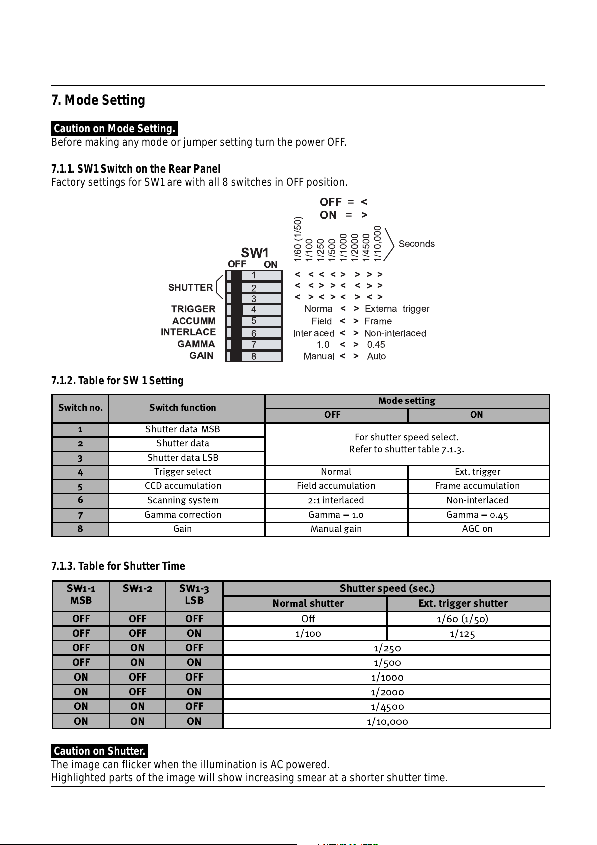
7.1.1. SW1 Switch on the Rear Panel
Factory settings for SW1 are with all 8 switches in OFF position.
OFF=<
ON
SHUTTER
TRIGGER
ACCUMM
INTERLACE
GAMMA
GAIN
OFF
SW1
ON
1
2
3
4
5
6
7
8
1/60 (1/50)
1/100
1/250
<
<
<
<
<
>
<
>
<
Normal
Field
Interlaced
1.0
Manual
1/500
<
>
>
<
>
<
<>
<>
<>
<>
<>
=
>
1/1000
1/2000
1/4500
1/10,000
>
>
>
<
>
>
>
>
<
External trigger
Frame
Non-interlaced
0.45
Auto
Seconds
7.1.2. Table for SW 1 Setting
Switch no. Switch function
1
2
3
4
5
6
7
8
Shutter data MSB
Shutter data
Shutter data LSB
Trigger select Normal Ext. trigger
CCD accumulation Field accumulation Frame accumulation
Scanning system 2:1 interlaced Non-interlaced
Gamma correction Gamma = 1.0 Gamma = 0.45
Gain Manual gain AGC on
7.1.3. Table for Shutter Time
SW1-1
MSB
SW1-2 SW1-3
LSB
OFF OFF OFF
OFF OFF ON
OFF ON OFF
OFF ON ON
ON OFF OFF
ON OFF ON
ON ON OFF
ON ON ON
Mode setting
OFF ON
For shutter speed select.
Refer to shutter table 7.1.3.
Shutter speed (sec.)
Normal shutter Ext. trigger shutter
Off 1/60 (1/50)
1/100 1/125
1/250
1/500
1/1000
1/2000
1/4500
1/10,000
Caution on Shutter.
The image can flicker when the illumination is AC powered.
Highlighted parts of the image will show increasing smear at a shorter shutter time.
- 15 -
Page 17

CV-M536/538/539
7.1.4. Ext. Trigger Shutter Mode
When trigger select SW1-4 is ON. The camera is in ext. trigger shutter mode. The SW1-1, SW1-2 and SW13 are for selecting the shutter speed. The range is from OFF to 1/10,000 second in 8 steps. For each
external trigger pulse, the camera will make an exposure with the selected shutter speed.
The shutter time setting is shown in “7.1.3. Table for Shutter Time”.
7.1.5. Trigger Select
SW1-4 is will select the camera operation mode.
OFF is normal mode, where the camera is running continuously.
ON is the ext. trigger shutter mode. Here the external trigger pulse will start the exposure.
7.1.6. CCD Accumulation
SW1-5 will select the CCD accumulation mode.
OFF is field accumulation. It is used for moving objects.
ON is frame accumulation. It is for still objects.
7.1.7. Scanning System
SW1-6 will select the scanning system.
OFF is 2.1 interlaced. It will follow the EIA or CCIR standard for interlaced scanning.
ON is non-interlaced.
In EIA the non-interlaced output is continuous ODD field. In CCIR the non-interlaced output is continuous
EVEN field.
If the camera is ext. HD/VD synchronized with a non-interlaced sync, SW1-6 be in ON position.
7.1.8. Gamma Correction
SW1-7 will select the gamma correction.
OFF is gamma 1.0. It is linear. Recommended for machine vision and image processing.
ON is gamma 0.45. It is non-linear.
7.1.9. Gain Control
SW1-8 is for gain select.
OFF is manual gain. Here the gain can be controlled by the GAIN potmeter on the rear panel.
ON is the AGC mode. Here the gain is adjusted automatically. The AGC level can be adjusted by VR3 on
PK8056 board. See “8. Adjustment of Video Signal Output Level”.
7.2. SW2 on PK8057 Board
This switch is to select 75 Ohm termination or TTL for ext. HD and ext. VD.
SW2-1 is for HD signal.
SW2-2 is for VD signal, or for ext. trigger in.
ON is 75 Ohm terminated. (Factory setting).
OFF is TTL level.
HD
ON
1
OFF
SW2
VD
2
- 16 -
Page 18
CV-M536/538/539
7.3. Jumper Settings
Caution on Jumper Setting.
Before making any mode or jumper setting turn the power OFF.
Jumpers for mode setting are found on the boards PK8054 & PK8057.
The following modes are available with jumper setting:
Input/Output Mode of HD/VD signal. (HD/VD input is factory setting)
Edge Pre-select Mode. (Factory setting)
Pulse Width Control Mode
Start/Stop Trigger Mode
Long Time Exposure Mode
Set the jumpers according to the list below in 7.3.1. and 7.3.2.
The jumper positions are shown in “7.4.1. Board 8054 Side B” and “7.4.2. Board 8057 Side A”.
Switch SW2 on PK8057 is shown in “7.2. SW2 on PK8057 Board”.
7.3.1. Jumper on PK8054 Board
HD/VD in/out External trigger modes
Jumper
R127
Ext.
HD/VD
input *)
Short
Int.
HD/VD
output
Short Short Short Open Short Factory set SHORT
Edge pre-
select
Pulse
width
control
Start/
stop
trigger
Long time
expose
Remarks
*) Factory Setting
7.3.2. Jumper on PK8057 Board
HD/VD in/out External trigger modes
Jumper
JP1
JP2
JP3
JP4
JP5
JP6
JP7
JP8
JP9
JP10
JP11
JP12
SW2-1
SW2-2
Ext.
HD/VD
input *)
Short
Open
Short
Open
Short
Open
Short
Open
Open
Open
Open
Short
ON
ON
Int.
HD/VD
output
Open Short Short Short Short HDinput /output. Factory set input
Short Open Open Open Open
Open Short Short Short Short VD input /output. Factory set input
Short Open Open Open Open
Short Short Short Short Short
Open Open Open Open Short Long time integration
Short Short Short Open Short
Open Open Open Short Open
Open Open Open Short Open
Open Open Open Short Open
- - - - - Pixel clock out. Factory set OPEN
Short Short Open Short Short Pulsewidth
- ON ON ON ON HD in 75 Ohm term. Factory set ON
- ON ON ON ON VD in 75 Ohm term. Factory set ON
*) Factory Setting
Edge pre-
select
Pulse
width
control
Start/
stop
trigger
Long time
expose
Remarks
HD input /output. Factory set input
VD input /output. Factory set input
7.3.3. Pixel Clock Output
To use pixel clock output (TTL level: 4.0 V), make the jumper JP11 on PK8057 board shorted-circuited. The
jumper position is shown in “7.4.1. Board PK8057 Side A”.
Pixel clock pulse will be output from pin no.9 of 12-pin multi-connector.
Caution for Pixel Clock Output.
When the pixel clock is enabled, it may cause interference with external equipment if it not properly
shielded.
- 17 -
Page 19
CV-M536/538/539
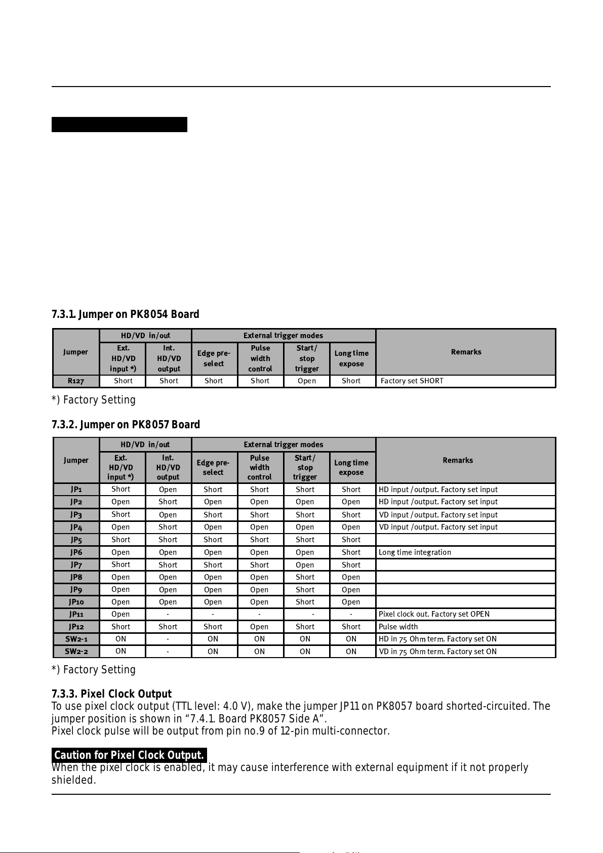
7.4. Location of SW2 and Jumpers
Jumpers are shorted with a 0 Ohm resistor or by a soldering between the 2 points. To remove the solder
tin from a jumper position, use a special tin remover such as de-soldering wick.
7.4.1. Board PK8054 Side B
7.4.2. Board PK8057 Side A
R127
JP10 JP2 JP1 SW2 JP6 JP7
JP9 1JP 2 JP4 JP3 JP5 JP8
JP11
- 18 -
Page 20
CV-M536/538/539
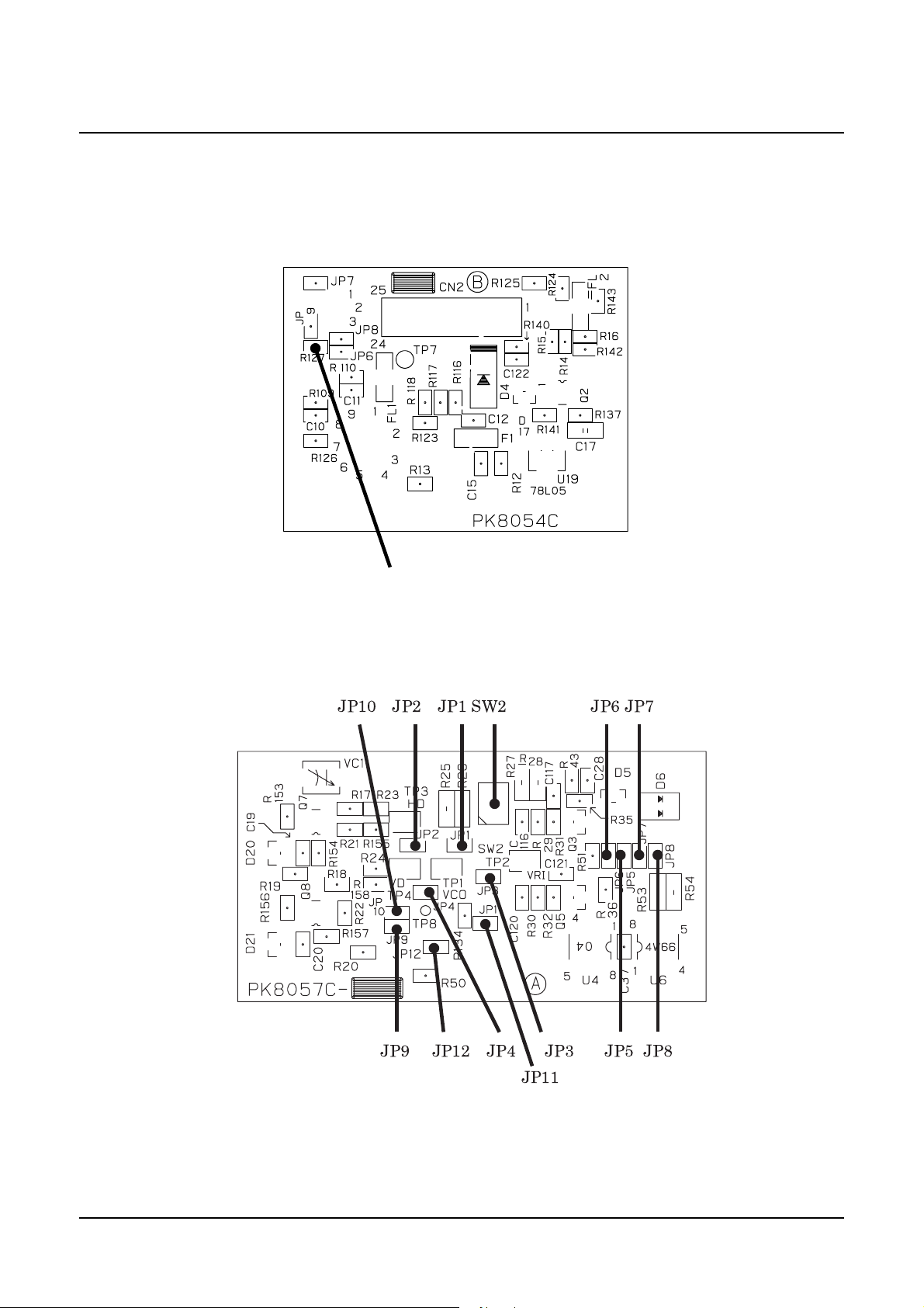
8. Adjustment of Video Signal Output Level
When an alignment of a video output signal is required, remove the camera housing and adjust
potentiometers VR3, VR4 and VR5 on the PK8056 board while measuring their levels at the video output
connector.
This adjustment should only be done in a setup with a standard TV test chart and controlled
illumination.
VR3: To adjust the gain level of AGC. (Factory setting: 700 mVp-p ± 30 mV)
VR4: To adjust the white level. (Factory setting: 800 mVp-p ± 20 mV)
VR5: To adjust the black level. (Factory setting: 20 mVp-p ± 5 mV)
CAUTION.
Do not touch these potentiometers unless you are familiar with camera adjustments.
Location of VR3 to VR5 on PK8056 board is as follow.
VR4 VR3 VR5
- 19 -
Page 21
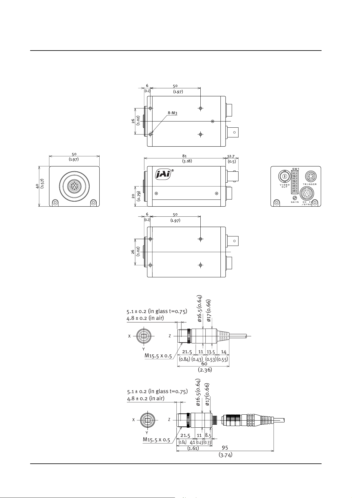
9. External Appearance
9.1 CCU
CV-M536/538/539
6
(0.2)
(1.02)(1.02)
50
(1.97)
8-M3
Unit : mm (inches)
40
(1.57)
9.2 HEAD
a)CV-M536
50
(1.97)
81
(3.18)
20 26
(0.79)
6 50
(0.2)
26
(1.97)
5.1 ± 0.2 (in glass t=0.75)
4.8 ± 0.2 (in air)
ø17(0.66)
ø16.5(0.64)
12.7
(0.5)
b)CV-M538/539
X
Y
M15.5 x 0.5
Z
(0.84) (0.43) (0.53)(0.55)
5.1 ± 0.2 (in glass t=0.75)
4.8 ± 0.2 (in air)
X
Y
M15.5 x 0.5
Z
21.5
(0.84) (0.43)(0.33)
- 20 -
11
41
(1.61)
13.5
1121.5
60
(2.36)
ø17(0.66)
ø16.5(0.64)
8.5
14
95
(3.74)
Page 22

10. Specifications
CV-M536/538/539
Scanning system CCIR 625 lines EIA 525 lines
CCD sensor Monochrome 1/2" Hyper HAD IT CCD
Sensing area 6.6 mm (h) x 4. 8 mm (v)
Effective pixels 752 (h) x 582 (v) 768 (h) x 494 (v)
Elements in video output 737 (h) x 575 (v) 758 (h) x 486 (v)
Cell size 8.6 (h) x 8.3 (v) µm 8.4 (h) x 9.8 (v) µm
Resolution (horizontal) 560 TV lines 570 TV lines
Resolution (vertical) 575 TV lines 485 TV lines
Sensitivity on sensor 0.05 lx
S/N ratio >56 dB (AGC off, Gamma 1)
Video output Composite VS signal 1.0 Vpp, 75 Ohm
Gamma 0.45 – 1.0
Gain Manual – Automatic. 0 to +15 dB by potentiometer or AGC
Scanning 2:1 interlace – non-interlace
Accumulation Field – frame
Synchronization Int. X-tal. Ext HD/VD or random trigger
HD sync. input/output 4V, 75 Ohm*
VD sync. input/output 4V, 75 Ohm*
Trigger input 4V, 75 Ohm*
Trigger input duration >HD interval
WEN output (write enable) 4V , 7 5 Oh m
EEN output (exposure enable) 4V, 75 Ohm
Pixel clock output (optional) 4V, 75 Ohm sine
Normal shutter Off, 1/100, 1/250, 1/500, 1/1000, 1/2000, 1/4500, 1/10,000 sec.
Edge pre-select shutter 1/60(1/50), 1/125, 1/250, 1/500, 1/1000, 1/2000, 1/4500, 1/10,000 sec.
Pulse width controlled shutter >1 H (64 µsec.) to <60 msec.
Start/stop trigger shutter 1/77 sec to 1/10,000 sec.
Long time exposure 1 field to ∞. Duration between ext. VD pulses
Operating temperature -5°C to +45°C
Humidity 20 – 80% non-condensing
Storage temp./humidity -25°C to 60°C/20 - 90%
Power 12V DC ±10%. 2.5W
Lens mount M15.5 x 0.5
Dimensions 40 x 50 x 80 mm (HxWxD)
Mass 230 g
25 frames/sec. 30 frames/sec.
* HD sync., VD sync./(Trigger) input or output by internal jumpers.
Factory setting: HD/VD input. Inputs TTL or 75 Ohm terminated by
internal jumpers. Factory setting: 75 Ohm terminated.
Note: Above specifications are subject to change without notice.
10.1. Spectral Sensitivity
1.0
0.8
0.6
0.4
Relative response
0.2
0.0
400 500 600 700 800 900
Wave length (nm)
1000
- 21 -
Page 23

CV-M536/538/539
11. Appendix
11.1. Precautions
Personnel not trained in dealing with similar electronic devices should not service this camera.
The camera contains components sensitive to electrostatic discharge. The handling of these devices
should follow the requirements of electrostatic sensitive components.
Do not attempt to disassemble this camera.
Do not expose this camera to rain or moisture.
Do not face this camera towards the sun, extreme bright light or light reflecting objects.
Even when this camera is not in use, put the supplied lens cap on the lens mount.
Handle this camera with the maximum care.
Operate this camera only from the type of power source indicated on the camera.
Power off the camera during any modification such as changes of jumper and switch setting.
11.2. Typical CCD Characteristics
The following effects may be observed on the video monitor screen. They do not indicate any fault of the
CCD camera, but do associate with typical CCD characteristics.
VV
. Smear. Smear
V
. Smear
VV
. Smear. Smear
Due to an excessive bright object such as electric lighting, sun or strong reflection, vertical smear may
be visible on the video monitor screen. This phenomenon is related to the characteristics of the
Interline Transfer System employed in the CCD.
VV
. A. A
liasingliasing
V
. A
liasing
VV
. A. A
liasingliasing
When the CCD camera captures stripes, straight lines or similar sharp patterns, jagged image on the
monitor may appear.
BlemishesBlemishes
Blemishes
BlemishesBlemishes
Some pixel defects can occur, but this does not have en effect on the practical operation.
Patterned NoisePatterned Noise
Patterned Noise
Patterned NoisePatterned Noise
When the CCD camera captures a dark object at high temperature or is used for long time integration,
fixed pattern noise (shown as white dots) may appear on the video monitor screen.
- 22 -
Page 24

12. User’s Record
Camera type: CV-M536/538/539
Scanning system: EIA/CCIR
Revision: (Revision E)
Serial No. .................
Users Mode Settings
Users Modifications
JAI A·S, Denmark
Produktionsvej 1, 2600 Glostrup
Copenhagen, Denmark
Phone +45 4457 8888
Fax +45 4491 8880
www.jai.com
JAI Corporation, Japan
German Industry Center
1-18-2 Hakusan, Midori-ku
Yokohama,
Kanagawa 226-0006, Japan
Phone +81 45 933 5400
Fax +81 45 931 6142
www.jai-corp.co.jp
JAI America, Inc., USA
Suite 450
23046 Avenida de la Carlota
Laguna Hills, CA 92653
USA
Phone +1 949 472 5900
Fax +1 949 472 5908
www.jai.com
2700-11096E E1 0201
 Loading...