

Page 1

Digital Monochrome Quad Speed
CMOS Progressive Scan Camera
CV-A33CL
Operation Manual
Camera: Revision A
Manual: Version 1.0
A33Manualsep09.doc
JPT 09-09-03
Page 2

CV-A33CL
Table of Contents
1. General ........................................................................................................2
2. Standard Composition ......................................................................................2
3. Main Features ................................................................................................2
4. Locations and Functions ................................................................................... 3
5. Pin Assignment............................................................................................... 4
5.1. 12-pin Multi-connector (DC-IN/Trigger) ....................................................................... 4
5.2. Digital Output Connector for Camera Link.................................................................... 4
5.3. Input and Output Circuits........................................................................................ 5
5.3.1. Trigger input................................................................................................ 5
5.3.2. EEN output .................................................................................................. 5
5.3.3. Camera Link interface .................................................................................... 6
6. Functions and Operations .................................................................................7
6.1. Basic functions .................................................................................................... 7
6.1.1. CMOS Sensor ................................................................................................ 7
6.1.2. Pixel principle .............................................................................................. 7
6.1.3. Column Process ............................................................................................ 8
6.1.4. CV-A33 CMOS Sensor array ............................................................................... 8
6.1.5. CMOS Sensor principle diagram.......................................................................... 8
6.1.6. Window of Interest ........................................................................................ 9
6.1.7. Auto Trigger Window of Interest. ....................................................................... 9
6.2. Sensor layout and timing. ......................................................................................10
6.2.1. Effective image format ..................................................................................10
6.2.2. Vertical timing ............................................................................................10
6.2.3. Horizontal timing .........................................................................................10
6.2.4. LVAL a-synchronous accumulation .....................................................................11
6.2.5. Timing for window of interest ..........................................................................12
6.3. Input/Output of Timing Signals ................................................................................13
6.3.1. Input of Timing Signals...................................................................................13
6.3.2. Output of Timing Signals.................................................................................13
6.4. Trigger Modes.....................................................................................................13
6.4.1. Continuous Operation (Non triggered) ................................................................14
6.4.2. Edge Pre-select Mode ....................................................................................14
6.4.3. Pulse Width Control Mode ...............................................................................16
6.4.4. Auto trigger Mode.........................................................................................17
6.5. Other Functions. .................................................................................................18
7. Configuring the Camera.................................................................................. 18
7.1. Switch setting inside ............................................................................................18
7.2. RS-232C control ..................................................................................................19
7.3. CV-A33CL command list.........................................................................................20
7.4. Camera Control Tool for CV-A33 ..............................................................................21
8. External Appearance and Dimensions ................................................................ 22
9. Specifications .............................................................................................. 22
9.1. Spectral sensitivity ..............................................................................................22
9.2. Specification table...............................................................................................23
10. Appendix .................................................................................................. 24
10.1. Precautions ......................................................................................................24
10.2. Typical Sensor Characteristics................................................................................24
11. Users Record.............................................................................................. 25
- 1 -
Page 3

CV-A33CL
1. General
The CV-A33CL is a digital CMOS camera designed for automated imaging applications, featuring
high speed within a uniform and compact housing.
The high-speed shutter function, asynchronous random trigger mode and partial scan mode, with
window of interest, allows the camera to capture high quality images of fast moving objects
with a high frame rate. The CV-A33CL features the Camera Link standardized multiplexed signal
output interface.
The latest version of this manual can be downloaded from: www.jai.com
The latest version of Camera Control Tool for CV-A33CL can be downloaded from: www.jai.com
For camera revision history, please contact your local JAI distributor.
2. Standard Composition
The standard camera composition consists of the camera main body and tripod mount plate.
3. Main Features
• 1/2” progressive scan monochrome CMOS sensor
• 659 (h) x 493 (v) 9.9 µm square pixels effective
• 10 or 8 bit video output in Camera Link
• 118.4 fps at full resolution
• 4953 frames/second for a 659 (h) x 3 (v) pixel image
• Programmable X and Y origin and size for window of interest
• Edge pre-select and pulse width external trigger modes
• Global shutter for instant full frame exposure
• Programmable shutter from 1 LVAL to 492 LVAL (16.8 µsec. to 8.3 msec.)
• Auto trigger function based on programmable 659 (h) x n (v) window
• Auto trigger frame rate up to 5403 frames/second
• Accepts standard C-mount lenses
• A-series platform
• Short ASCII commands for fast mode setup via serial port
• Setup by Windows 98/NT/2000 software via RS 232C or Camera Link
- 2 -
Page 4
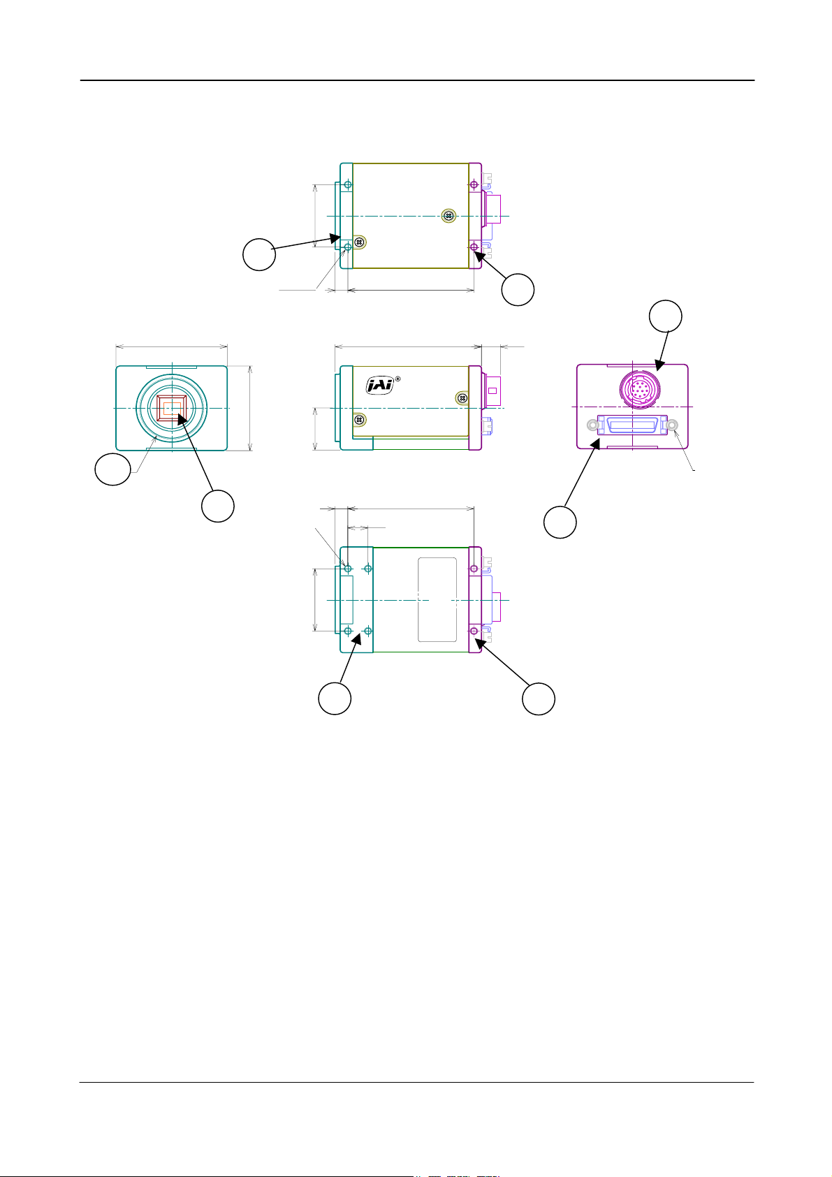
4. Locations and Functions
C-Moun t
2
5
4xM3 Depth 4
44
(1 .73 )
35
(1 .38 )
1
4xM3 Depth 4
1. CMOS sensor
2. Lens mount (C-mount)
3. Digital output connector (Camera Link)
4. DC in/Trigger in/RS-232C connector
5. Mounting holes M3. Depth 4. (10x)
4-M3深4
(0 .2 )
M3深4
6-
26
17 .5
26
CV-A33CL
(1 .02 )
5
(0 .2 )
(0 .69 )
5
8
(0 .31 )
(1 .02 )
5
Fig. 1. Locations
50
(1 .97 )
58
(2 .28 )
50
(1 .97 )
5
4
7.6
(0 .3 )
IN /DC
TR IG
/ODIGITAL I
U4-40
コネクター固定ネジ
3
機銘版
5
- 3 -
Page 5
CV-A33CL
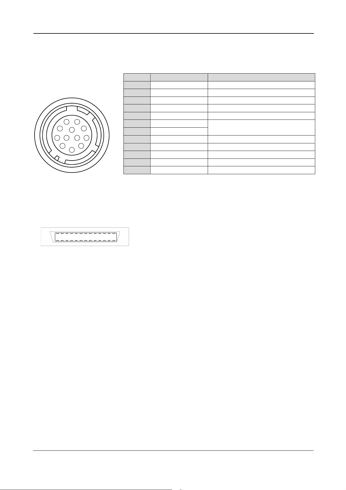
5. Pin Assignment
5.1. 12-pin Multi-connector (DC-IN/Trigger)
Type: HR10A-10R-12PB-01
(Hirose) male.
(Seen from rear of camera.)
9
1
2
11
3
4
8
10
7
12
6
5
Fig. 2. 12-pin connector.
Refer to 7.1. Inside switch settings.
Pin no. Signal Remarks
1 GND
2 +12 V DC input
3 GND
4 N/C
5 GND
6 RXD in
7 TXD out
8 GND
9 EEN out
10 Trigger input
11 N/C
12 GND
*) Internal SW300-1 on rear board for 75 Ω terminations.
RS 232C. Or via Camera Link by internal
SW200 on PK8378A (Off=HR)
And via Camera Link
Or via Camera Link. (TI=1 for HR) *)
5.2. Digital Output Connector for Camera Link
13
26
1
14
Fig. 3. Camera Link connector
The digital output signals follow the Camera Link standardized multiplexed signal output
interface. Camera Link base configuration is used. The interface circuit is build around the NS
type DS90CR285MTD.
The following signals are found on the Digital Output Connector:
SerTC RXD serial data to camera
SerTFG TXD serial data to frame grabber
CC1 Trigger input
CC2 Factory use
X0 to X3 Camera Link multiplexed data out
Xclk Camera Link clock. Used as pixel clock.
In the Channel Link X0 to X3 multiplexed signals the following signals are encoded.
D0 – D9 2 x 8/10 bit video data out.
LVAL Line VALid. Video line data is valid. High for valid line.
FVAL Frame VALid. Video frame data is valid. High for valid frame.
DVAL Data VALid. Effective video pixel data is valid. High for valid data.
EEN Exposure ENable. High during exposure.
The polarity is positive and TRIG in negative as factory setting.
For Camera Link interface principle diagram please check Fig. 7.
Type: 26 pin MRD connector
3M 10226-1A10JL
(Or via 12 pin HR by internal SW200.
On for CL)
(Or on 12 pin HR. TI=0 for CL)
- 4 -
Page 6
CV-A33CL
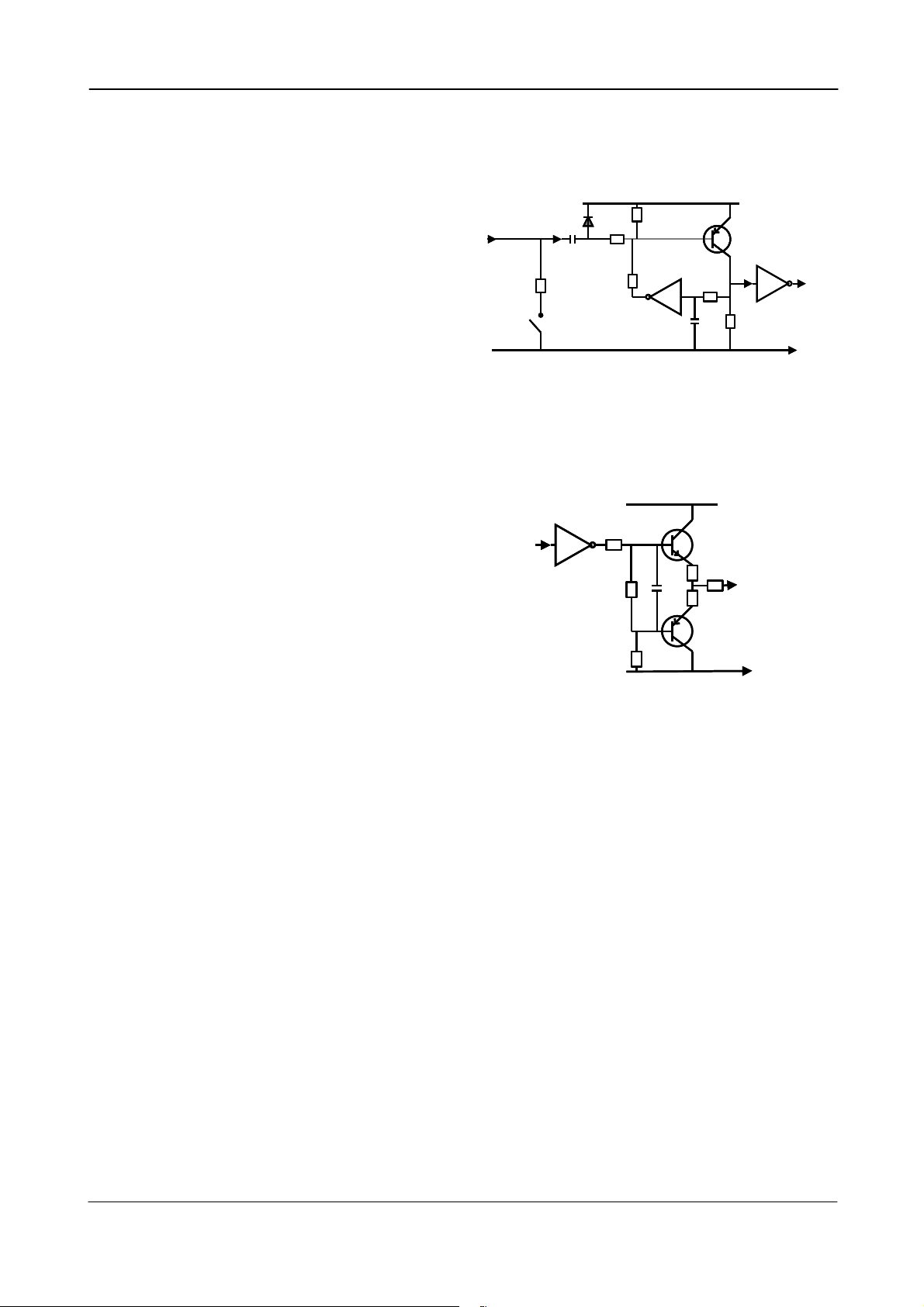
5.3. Input and Output Circuits
5.3.1. Trigger input
The trigger inputs on pin #10 12 pin Hirose
connector is AC coupled. To allow a long pulse
width, the input circuit is a flip flop, which is
toggled by the negative or positive
differentiated spikes caused by the falling or
rising trigger edges.
The trigger polarity can be changed.
Trigger input level 4 V ±2 V. It can be 75Ω
terminated by internal SW300 on PK8388A.
The trigger inputs can be changed to
Camera Link input. (TI=0 for CL)
Fig. 4. Trigger input.
Trig input
Trig input
pin #10
pin #10
GND
GND
100n
100n
75Ω
75Ω
SW 300
SW 300
1k
1k
15k
15k
68k
68k
1n
1n
100k
100k
+5V
+5V
1k
1k
TTL
TTL
GND
GND
5.3.2. EEN output
On pin #9 on 12 pin HR connector EEN The output
circuit is 75 Ω complementary emitter followers. It
will deliver a full 5 volt signal.
Output level ≥4 V from 75Ω. (No termination).
EEN is also found in Camera Link.
Fig. 5. EEN output
TTL
TTL
100
100
2k2
2k2
10k
10k
+5V
+5V
75
75
2
2
2
2
#9/12
#9/12
EEN output
EEN output
GND
GND
- 5 -
Page 7
CV-A33CL
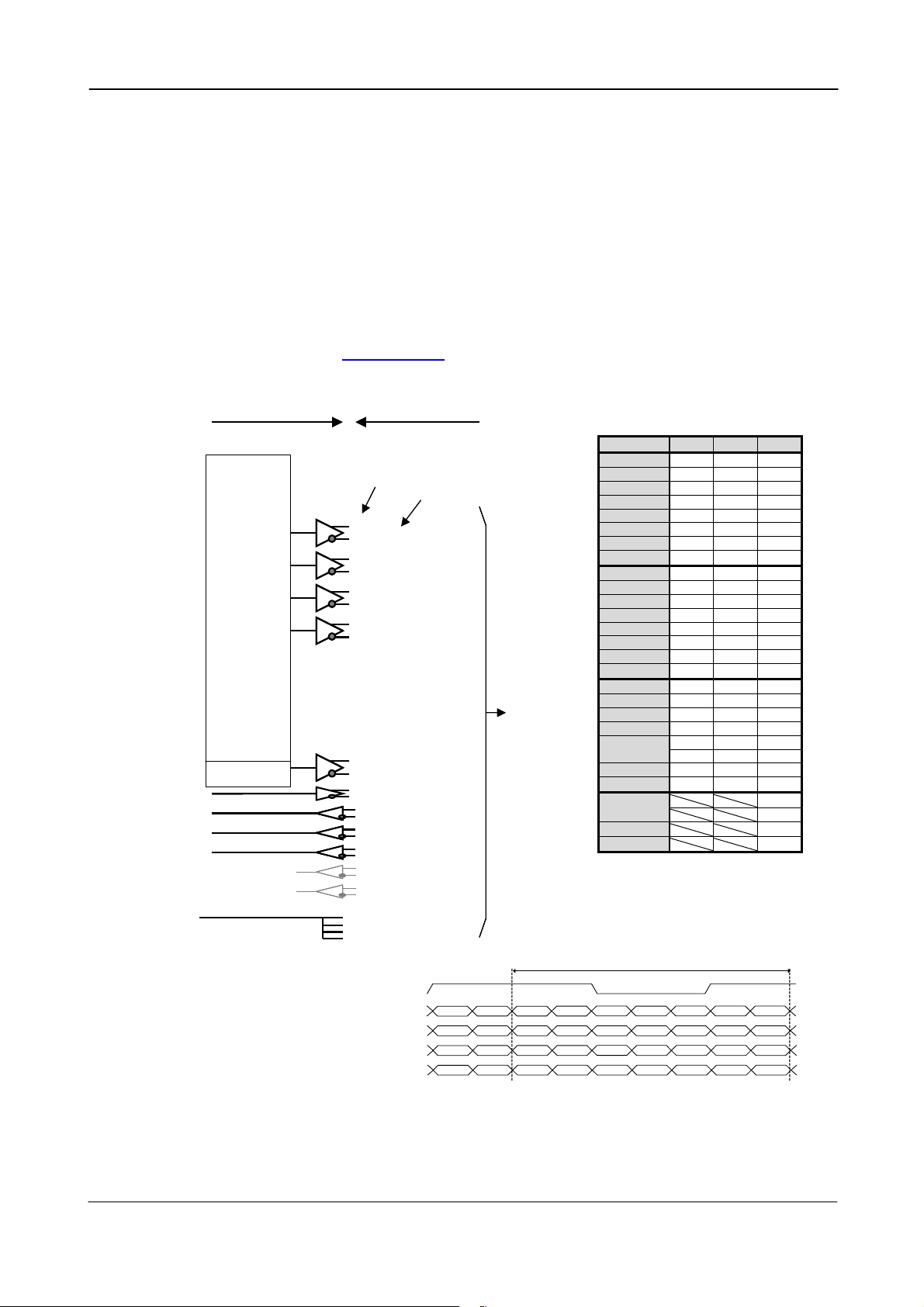
5.3.3. Camera Link interface
The video output is Camera Link with 10 or 8 bit video placed in a base configuration. The digital
output signals follow the Camera Link standardized multiplexed signal output interface. The
Camera Link output driver is NS type DS90CR285MTD.
The data bits from the digital video, FVAL, LVAL, DVAL and EEN are multiplexed into the twisted
pairs, which are a part of the Camera Link. Trigger signals and the serial camera control are
feed directly through its own pairs. The trigger input can also be TTL on the 12 pin connector.
(TI=0 for CL. TI=1 for 12 pin HR). The serial camera control can be switches between the 12 pin
connector or CL by the internal switch SW200 on PK8387B.
The 26 pin MDR connector pin assignment follows the Camera Link base configuration.
For a detailed description of Camera Link specifications, please refer to the Camera Link
standard specifications found on www.jai.com
CV-A33 Camera Camera Link Cable
Camera Signals
Camera Signals
8bit 10bit
8bit 10bit
D2 D0
D2 D0
D3 D1
D3 D1
D4 D2
D4 D2
D5 D3
D5 D3
D6 D4
D6 D4
D7 D5
D7 D5
D8 D6
D8 D6
D9 D7
D9 D7
NC D8
NC D8
NC D9
NC D9
NC NC
NC NC
NC NC
NC NC
NC NC
NC NC
NC NC
NC NC
NC NC
NC NC
NC NC
NC NC
NC NC
NC NC
NC NC
NC NC
NC NC
NC NC
NC NC
NC NC
NC NC
NC NC
NC NC
NC NC
NC NC
NC NC
NC NC
NC NC
LVAL
LVAL
FVAL
FVAL
DVAL
DVAL
EEN
EEN
Pclk
Pclk
TXD out
TXD out
RXD in
RXD in
Ext. trig 1 in
Ext. trig 1 in
Ext. Trig 2 in
Ext. Trig 2 in
Ground
Ground
CV-A33 Camera Camera Link Cable
Camera Link
Camera Link
Pin
Pin
A 0 Tx0
A 0 Tx0
A1 Tx1
A1 Tx1
A2 Tx2
A2 Tx2
A3 Tx3
A3 Tx3
A4 Tx4
A4 Tx4
A 5 Tx6
A 5 Tx6
A 6 Tx27
A 6 Tx27
A 7 Tx5
A 7 Tx5
B 0 Tx7
B 0 Tx7
B 1 Tx8
B 1 Tx8
B 2 Tx9
B 2 Tx9
B 3 Tx12
B 3 Tx12
B 4 Tx13
B 4 Tx13
B 5 Tx14
B 5 Tx14
B 6 Tx10
B 6 Tx10
B 7 Tx11
B 7 Tx11
C 0 Tx15
C 0 Tx15
C 1 Tx18
C 1 Tx18
C 2 Tx19
C 2 Tx19
C 3 Tx20
C 3 Tx20
C 4 Tx21
C 4 Tx21
C 5 Tx22
C 5 Tx22
C 6 TX16
C 6 TX16
C 7 Tx17
C 7 Tx17
Tx24
Tx24
Tx25
Tx25
Tx26
Tx26
Tx23
Tx23
Txclk
Txclk
4 x
4 x
7-1
7-1
MUX
MUX
Connector pin
Connector pin
15
15
2
2
16
16
3
3
17
17
4
4
19
19
6
6
18
18
5
5
21
21
8
8
7
7
20
20
22
22
9
9
10
10
23
23
24
24
11
11
12
12
25
25
1
1
14
14
13
13
26
26
X0
X0
X1
X1
X2
X2
X3
X3
Xclk
Xclk
SerTFG
SerTFG
SerTC
SerTC
CC1
CC1
CC2
CC2
CC3
CC3
CC4
CC4
Sheilds
Sheilds
TxCLK
TxOUT3
TxOUT2
TxOUT1
TxOUT0
Fig. 7. Principle diagram for Camera Link base configuration interface
Signal
Signal
Sheilds
Sheilds
Pair 1
Pair 1
Pair 2
Pair 2
Pair 3
Pair 3
Pair 5
Pair 5
Pair 4
Pair 4
Pair 7
Pair 7
Pair 6
Pair 6
Pair 8
Pair 8
Pair 9
Pair 9
Pair 10
Pair 10
Pair 11
Pair 11
A7
C3
B2
A1
Frame
Frame
Grabber
Grabber
A6
C2
B1
A0
To
To
EEN
DVAL
Port/Signal 8bit 10bit Pin No.
Port A0 D2 D0 Tx0
Port A1 D3 D1 Tx1
Port A2 D4 D2 Tx2
Port A3 D5 D3 Tx3
Port A4 D6 D4 Tx4
Port A5 D7 D5 Tx6
Port A6 D8 D6 Tx27
Port A7 D9 D7 Tx5
Port B0 NC D8 Tx7
Port B1 NC D9 Tx8
Port B2 NC NC Tx9
Port B3 NC NC Tx12
Port B4 NC NC Tx13
Port B5 NC NC Tx14
Port B6 NC NC Tx10
Port B7 NC NC Tx11
Port C0 NC NC Tx15
Port C1 NC NC Tx18
Port C2 NC NC Tx19
Port C3 NC NC Tx20
Port C4 NC NC Tx21
Port C5 NC NC Tx22
Port C6 NC NC Tx16
Port C7 NC NC Tx17
Camera Link bit allocation
LVAL Tx24
FVAL Tx25
DVAL Tx26
EEN Tx23
D0 = LSB. D9 = MSB
C7
FVAL
C0
C1
A5
B0
1 pixel cycl e
C6
LVAL
B5
A4
Timing
B6
B7
C4
C5
B3
B4
A2
A3
A6
A7
C2
C3
B1
B2
A0
A1
- 6 -
Page 8
CV-A33CL
6. Functions and Operations
In the following the format shown in “7.3. CV-A33CL command list” are used for function
commands and parameters.
6.1. Basic functions
The CV-A33CL camera is a progressive scan camera with 10 or 8 bit video output in single
channel Camera Link.
Programmable partial scan, where the start line and the number of lines can be selected with 1
line increment is also available.
There are 4 modes: Normal continuous, and 3 trigger modes: Edge Pre-Select (EPS), Pulse Width
Control (PWC) and Auto Trigger.
The accumulation is LVAL a-synchronous.
In the following some of the functions are shown in details.
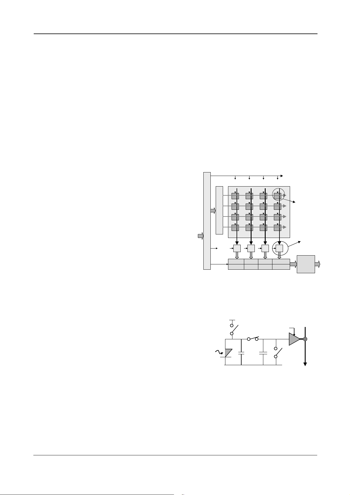
6.1.1. CMOS Sensor
The CMOS sensor principle layout is shown.
The sensor is an array of active photosensitive
R
pixels. The global shutter is working
simultaneously on all pixels. The readout can be
random row by row. 4 columns are feed through
a 4 to 1 multiplexer to an A/D converter. The
digitized row signals are placed in a vertical
register by a 1 to 4 multiplexing. From here it is
read out with the pixel clock pulses, even if the
window of interest has fewer columns. The
frame speed depends only of the height of the
window, not of the width.
Pixel principle and column processing with A/D
converting is shown below.
Control
Control
and
and
set up
set up
R
O
O
T
T
W
W
I
I
D
D
M
M
E
E
I
I
C
C
N
N
O
O
G
G
D
D
E
E
2 x 10 bit digital shift register
2 x 10 bit digital shift register
Fig. 7. CMOS principle layout
Pixel
Pixel
Column
Column
Process
Process
and A/D
and A/D
Video
Video
process
process
6.1.2. Pixel principle
Each pixel consists of a sensing part, a pixel memory
and an amplifier. The function can in short be
described. The photo diode and charge capacitor is
reset when switch 1 is closed. The signal accumulation
starts when sw 1 open. The charge is transferred to the
pixel memory capacitor when sw 2 close. The
accumulation stop when sw 2 open, and the signal is
now temporary stored in the memory capacitor. After
Start exposure Stop exposure
Start exposure Stop exposure
12
12
Light
Light
Photo
Photo
diode
diode
Charge
Charge
capacitor
capacitor
Pixel
Pixel
memory
memory
Read row
Read row
3
3
Reset
Reset
memory
memory
4
4
Buffer
Buffer
amplifier
amplifier
To column
To column
processing
processing
reset of the charge capacitor, a new accumulation can
start. The signal on the pixel memory capacitor is read
out to the column by the read row signal. The memory
Fig. 8. Pixel principle.
can now be reset.
With this construction all pixels will integrate at the same time, (Global shutter). The resulting
image is temporary stored in the pixel memory during read out, while a new exposure can be
started.
All timing is set up in the timing block by an internal serial link.
- 7 -
Page 9

CV-A33CL
6.1.3. Column Process
The voltage signal from a single pixel is send to the
column amplifier trough the 4 to 1 multiplexer. After
the S/H circuit, the offset and gain calibrating is
perform. A 10 bit A/D converter send the digital pixel
signal to the digital horizontal shift register by a 1 to 4
multiplexing. Signals from a single row with 667 pixels
are processed in parallel and send to the shift register.
Control and timing is done from the timing block.
The calibrate command CB = 0 will start an automatic
calibrate routine for offset and gain for all 167 A/D
converter. It reduces the vertical fix pattern column noise.
6.1.4. CV-A33 CMOS Sensor array
The CMOS sensor total array is 667 (h) x 502 (v).
Here the 659 (h) x 494 (v) is active photo sensing
pixels. 8 pixels (h) and 8 rows (v) are optical
black pixels for internal black level reference.
There is an A/D converter for each 4 columns.
A 4 to 1 multiplexer feed the signals from 4
columns to a A/D converter. The digital
converter output is multiplexed to the 667 x10
bit register.
Columns
Columns
(502,667)
(502,667)
Timing
Timing
Fig. 10. CV-A33 CMOS sensor array
Amp
Amp
Offset
Gain
Gain
calibr
calibr
Control and timing
Control and timing
A/DS/H
A/DS/H
Offset
Fig. 9. Column processing principle
8 rows and 8 columns
667 Columns
667 Columns
667 x 502 sensor array
667 x 502 sensor array
659 x 494 Active pixels
659 x 494 Active pixels
Row decode
Row decode
4 to 1 multiplexer
4 to 1 multiplexer
167 x A/D converter
167 x A/D converter
1 to 4 multiplexer
1 to 4 multiplexer
667 x 10 bit register
667 x 10 bit register
8 rows and 8 columns
optical dark pixels
optical dark pixels
502
502
Rows
Rows
(1,1)
(1,1)
10 bit digital
10 bit digital
Video out
Video out
10 bit
10 bit
video
video
To shift
To shift
Register
Register
through
through
1 to 4
1 to 4
multiplex
multiplex
6.1.5. CMOS Sensor principle diagram
Fig. 11. CMOS sensor principle diagram
- 8 -
Page 10

CV-A33CL
6.1.6. Window of Interest
If a higher frame rate is wanted, it is possible to change
the CMOS sensors sensing area to the window of
interest. WS =1 for windows scan.
The X,Y start coordinate, the window width and height
can be programmed.
WX can be in the range 0 to 657
WY can be in the range 0 to 490
WW can be in the range 2 to 659. (WX + WW ≤ 659)
WH can be in the range 3 to 493. (WY + WH ≤ 493)
The frame rate will not increase if the width WW is
reduced. The horizontal shift register need to be read
out in its full length.
Minimum size for the window of interest is 2 (h) x 3 (v)
pixels.
Maxim frame rate is 4953 fps.
For DVAL timing details for the window of interest,
refer to 6.2.5 fig. 17 through 19.
WY
WY
LVAL
LVAL
DVAL
DVAL
0,0
0,0
WX
WX
X,Y
X,Y
WW
interest
interest
WH
WH
WW
Window of
Window of
Fig. 12. Windows of Interest
FVAL
FVAL
6.1.7. Auto Trigger Window of Interest.
The auto trigger function, TR=3 can be used as sensing device inside the camera field of view.
The scanned area is from top of the image, and the height can be programmed with the
command AT= --. The accumulation time is equal to the number of LVAL programmed with AT.
The minimum height of the window of interest for the auto trigger function is the 3 top lines of
the image. The height of the auto trigger window can be programmed in the range AT = 3 to
493. The window is always from the top of image. The read out time is the active number of
LVAL + 9 LVAL.
Maxim frame rate is 5403 fps given by the 11 LVAL for a minimum window read out.
(1 LVAL = 16.825 µsec.)
The connected frame grabber should be programmed to sense if objects passing the window.
The horizontal position and the signal threshold could be the programmed parameters. If an
object passing is detected, a trigger is send to the camera, and a full frame is exposed with the
same accumulation time as programmed for AT. The resulting image, a full frame or windows
scan, (depending of windows scan setting), is read out to the grabber, and the auto trigger
function will start again.
- 9 -
Page 11

CV-A33CL
6.2. Sensor layout and timing.
6.2.1. Effective image format
The drawing below shows the effective pixels on the CCD array with respect to pixels and lines
as it is used in the timing and video read out.
(0, 0)
Minimum
window size
3
2
Active Pixel Array
493
6.2.2. Vertical timing
Normal mode. Full frame.
FVAL
LVAL
(When t he exposur e i s max . ( PE=493) )
Exposur e
per i od
EEN
(When t he exposur e i s mi n. ( PE=2) )
Exposur e
per i od
EEN
DAT A OUT
DVAL
0
1234
……
659
(658, 492)
Fig. 13. Effective image layout
1 F VAL pe r i o d
502L
498L
Ef f ect i ve Li nes
493L
……
1 LVAL = 16.825 µs
4L
5L
9
8
0
2
1
8
8
9
9
9
4
4
4
4
4
4L
01234
……
6.2.3. Horizontal timing
Normal mode. Full frame.
L VAL
9ck
DAT A OUT
DVAL
0
1234
Fig. 14. Vertical timing
1 LVAL per i od
673ck
668ck
Ef f ec t i v e Pi x e l s
……
659ck
……
Fig. 15. Horizontal timing
- 10 -
1 ck = 25 ns
5ck
5ck
5
4
7
8
6
5
5
5
5
5
6
6
6
6
6
9ck
012
……
Page 12

CV-A33CL
6.2.4. LVAL a-synchronous accumulation
The CV-A33CL has LVAL a-synchronous accumulations only. The accumulation will start 28 µsec.
after the trigger leading edge. EEN will indicate the accumulation time. When the accumulation
stops after the selected shutter time, the LVAL phase is reset and restarted.
1 LVAL = 16.825 µsec.
16.8 µsec.
16.8 µsec.
LVAL
LVAL
LVAL
Trigger
Trigger
Trigger
Accum
Accum
Accum
Delay 28 µsec.
Delay 28 µsec.
Delay 28 µsec.
EEN
EEN
EEN
Fig. 16. LVAL a-synchronous accumulation
In CV-A33 with LVAL a-synchronous accumulation a new trigger can be input and start a new
exposure during the previous frame read out. But the exposure may not be finished before the
frame is read out. It makes it possible to have a trigger rate close to the frame rate.
The minimum trigger interval should be >(1FVAL + 1 LVAL).
- 11 -
Page 13

CV-A33CL
6.2.5. Timing for window of interest
With WS=1, the X and Y start coordinates (WX and WY), and the width and height (WW and WH)
for the window of interest can be programmed with 1 pixel interval. The minimum window size
is 2(h) x 3 (v). If the window is specified outside the full image area, it will be placed up to the
right or low limit as shown in fig 17. right.
Figures marked with (*) in the timing diagrams below will change with other window settings.
(0, 0)
(200, 100)
120
240
Active Pixel Array
659
493
(658, 492)
Fig. 17. Window of interest.
FVAL
(0, 0)
1 FVAL per i od
129L( * )
125L( * )
Active Pixel Array
(559, 393)
659
100
100
493
Readout Region
(WX=559, WY=393, WW=100, WH=100)
Specifyed Region
(WX=600, WY=400, WW=100, WH=100)
(658, 492)
1 LVAL = 16.825 µs
(*) Vari abl e Number
4L
L VAL
DAT A OUT
DVAL
L VAL
DAT A OUT
DVAL
Ef f ect i ve Li nes
4
3
2
1
0
0
0
0
0
0
……
1
1
1
1
1
120L( * )
……
Fig. 18. Vertical timing for window of interest.
1 LVAL per i od
673ck
668ck
9ck
200ck( * )
Ef f ect i ve Pi xel s
240ck( * )
2
1
0
……
0
0
0
2
2
2
……
4
219ck ( *)
9
8
7
3
3
3
4
4
Fig. 19. Horizontal timing for window of interest.
5L 4L
8
5
9
6
7
1
1
1
1
1
2
2
2
2
2
4
3
2
1
0
0
0
0
0
0
……
1
1
1
1
1
1 ck = 25 nsec
(*) Vari abl e Number
5ck
5ck
9ck
- 12 -
Page 14

CV-A33CL
6.3. Input/Output of Timing Signals
6.3.1. Input of Timing Signals
It is not possible to synchronize the camera from an external sync source except by an extern
trigger pulse. The camera will always run with its internal X-tal controlled timing.
Trigger input through Camera Link. TI=0
Trigger input as TTL on pin #10 on 12 pin Hirose. TI=1
The trigger polarity is active low. TP=0
Trigger input can be changed to active high. TP=1
The trigger input on pin #10 on the 12 pin Hirose connector can be 75 Ω terminated with the
internal switch SW 300-1 ON.
6.3.2. Output of Timing Signals
To synchronize the video data transfer from the camera the following signals are available in a
base configuration of Camera Link:
FVAL Frame valid High for valid Frame
LVAL Line valid High for valid line
PCLK Pixel clock
DVAL Data valid High for valid data
EEN Exposure enable Low during exposure
See the full connector pin assignment for Camera Link in chapter 5.3 and 5.4.5
For complete documentation on the Camera Link standard, please contact your JAI distributor.
EEN is also found as a TTL signal on pin #9 on the 12 pin Hirose. EEN is low during exposure.
6.4. Trigger Modes
This camera can operate in 4 primary modes. 1 non-triggered, 2 external asynchronous trigger
modes and auto trigger mode.
1. Normal continuous Mode. TR=0 Pre-selected exposure. (SM=0, SM=1)
2. Edge Pre-select Mode. TR=1 Pre-selected exposure. (SM=0, SM=1)
3. Pulse Width Control Mode. TR=2 Pulse width controlled exposure.
4. Auto Trigger Mode. TR=3 >3 line window, <5404 fps
In normal continuous mode (TR=0) and edge pre-select mode (TR=1) the shutter time can be
selected from the normal 8 fixed steps (SM=0), or it can be selected from the 2 to 493 steps
programmable (SM=1). In programmable exposure the actual exposure is 1 LVAL less than the PE
value.
The trigger pulse width should be >1 LVAL to <3 FVAL. (>16.8 µsec. to <25 msec.)
In pulse width control (TR=2) the trigger pulse width should be >1 LVAL to <237 FVAL. (>16.8
µsec. to <2 sec.)
Windows of interest (WS=1) can be used in normal, edge pre-select and pulse width control
mode. (TR=0, TR=1 and TR=2).
- 13 -
Page 15

CV-A33CL
6.4.1. Continuous Operation (Non triggered)
Mode settings can be done with RS-232C. Trigger Mode Normal. TR=0. It is for applications where
the camera is continuous running without external trigger. The shutter mode can be normal or
programmable exposure. (SM=0, SM=1). The shutter will work in all 8 steps up to 1/20,000
second or with the programmable exposure in 2 to 493 steps. In programmable exposure the
actual exposure is 1 LVAL less than the PE value.
In windows scan (WS=1), shutter times longer than the actual frame time have no meaning. The
exposure will be equal the frame time.
To use this mode:
Set function: Trigger mode “Normal” TR=0
Shutter mode “Normal” or “Programmable” SM=0, SM=1
“Shutter Speed” SH=0 through 7
“Programmable exposure” PE=2 through 493
“Windows” “Full” or “Windows scan” WS=0, WS=1
Polarity and other functions
Important notes on using this mode.
• The line at the end of the exposure period (SM=0, SM=1) will have a slightly lower signal
level. (About 10%). It is caused by the CMOS. (With SH=1/250 the line is seen in the
middle of the image).
For timing refer to 6.2.2. and 6.2.3. Fig. 14. and fig 15.
For windows scan timing refer to 6.2.5 and fig.17 through fig.19.
6.4.2. Edge Pre-select Mode
The exposure will start 28 µsec. after the trigger leading edge, and it stops and is read out after
the shutter time selected. It can be the 8 steps in normal or 2 to 493 steps in programmable.
SM=0 or SM=1. In programmable exposure the actual exposure is 1 LVAL less than the PE value.
This mode will operate with full window or windows of interest scanning.
An EEN pulse will indicate the active accumulation time, and a FVAL pulse indicates that the
resulting video is read out.
To use this mode:
Set function: Trigger mode “Edge Pre-select” TR=1
Shutter mode “Normal” or “Programmable” SM=0, SM=1
“Shutter Speed” SH=0 through 7
“Programmable exposure” PE=2 through 493
“Windows” “Full” or “Windows scan” WS=0, WS=1
Polarity and other functions
Input: Ext. trigger to Camera Link or pin 10 on 12-pin connector.
Important notes on using this mode.
• The duration of the trigger should be >1 LVAL to <3 FVAL. (>16.8 µsec. to <25 msec.)
• A new trigger can be applied before FVAL is low as long as the exposure will be on for
longer than the FVAL high period. Refer to 6.2.4
For timing refer to 6.2.2. and 6.2.3. Fig. 14. and fig 15.
For windows scan timing refer to 6.2.5 and fig.17 through fig.19.
For LVAL a-synchronous accumulation refer to 6.2.4 and fig 16.
- 14 -
Page 16

TRG
FVAL
LVA L
xposu re
pe r iod
EEN
DATA OUT
CV-A33CL
(When the exposureismin.(PE=2))
2L
27 .6 μS
Effective Lines
01234
……
1FVALperiod
502L
498L
493L
……
1 LVAL = 16.825µs
5L
0
9
8
2
1
8
8
9
9
9
4
4
4
4
4
2L
DVA L
TRG
FVA L
LVA L
xposu re
pe r iod
EEN
DATA OUT
DVA L
Fig. 20. Vertical timing for edge pre-select min. exposure
(When the expo sureismax.(PE=493))
27 .6 μS
Fig. 21. Vertical timing for edge pre-select max. exposure
2L
01234
……
1FVALperiod
502L
498L
Effective Lines
493L
1 LVAL = 16.825µs
5L
0
9
1
8
……
2
8
9
9
9
8
4
4
4
4
4
2L
- 15 -
Page 17

CV-A33CL
6.4.3. Pulse Width Control Mode
The exposure will start 28 µsec. after the trigger leading edge, and it stops and is read out at
the trigger trailing edge. This mode will operate with full window or windows of interest
scanning.
An EEN pulse will indicate the active accumulation time, and a FVAL pulse indicates that the
resulting video is read out.
To use this mode:
Set function: Trigger mode “Pulse Width Control” TR=2
“Windows” “Full” or “Windows scan” WS=0, WS=1
Polarity and other functions
Input: Ext. trigger to Camera Link or pin 10 on 12-pin connector.
Important notes on using this mode.
• The duration of the trigger should be >1 LVAL to <237 FVAL. (>16.8 µsec. to <2.0sec.)
The image quality can be reduced at maximum pulse width.
• A new trigger can be applied before FVAL is low as long as the exposure will be on for
longer than the FVAL high period. Refer to 6.2.4
For timing refer to 6.2.2. and 6.2.3. Fig. 14. and fig 15.
For windows scan timing refer to 6.2.5 and fig.17 through fig.19.
For LVAL a-synchronous accumulation refer to 6.2.4 and fig 16.
1 LVAL = 16.825µs
TRG
FVAL
LVA L
xposu re
pe r iod
EEN
DATA OUT
DVA L
27 .6 μS
1FVALperiod
2L
01234
……
502L
498L
Effective Lines
493L
Fig. 22. Vertical timing for pulse width control min. exposure
……
2L
5L
2
0
1
9
8
9
8
9
9
8
4
4
4
4
4
- 16 -
Page 18

CV-A33CL
WhenTrggerisinput
6.4.4. Auto trigger Mode
The auto trigger function, TR=3 can be used as sensing device inside the camera field of view. It
sense in a programmable window from top of the image. The continuous output is sent to the
frame grabber, which PC should be programmed to sense if an object is passing the window. The
horizontal position and the signal threshold could be the programmed parameters. If an object
passing is detected, a trigger is send to the camera. The resulting image, a full frame or
windows scan, (depending of windows scan setting), is read out to the grabber, and the auto
trigger function with fast scan of the programmed window will start again.
To use this mode:
Set function: Trigger mode “Auto Trigger Mode” TR=3
“Auto Trigger” AT=3 through 493
“Windows” “Full” or “windows scan” WS=0, WS=1
Polarity and other functions
PC and grabber: Detect trigger conditions
Send a pulse width control trigger to the camera.
Input: Ext. trigger to Camera Link or pin #10 on 12-pin connector.
Important notes on using this mode.
• The exposure is equal the programmable parameter AT.
• The exposure time is the same for the auto trigger partial scanned frame and the
resulting triggered frame read out.
• The duration of the trigger should be >1 LVAL to < 1 FVAL. (>16.8 µsec. to <8.3 msec.)
• Refer to 6.1.7. Auto Trigger Window of Interest.
• Max auto trigger frame rate is 5403 fps.
1FVALperiod
11L
TRG
1FVALperiod
502L
.
1 LVAL = 16.825µs
FVA L
LVA L
xposu re
pe r iod
EEN
DATA OUT
DVA L
E f fec t ive P ixe ls
4L
3L
012
Effective Lines
4L
0
012
012
34
12
493L
0
8
9
1
9
8
8
9
4
4
4
4
4
4L
5L
2
9
012
012
012
Fig. 23. Vertical timing for auto trigger function
- 17 -
Page 19

CV-A33CL
6.5. Other Functions.
User ID.
The command (UD) the user can save up to 16 characters in the camera to identify the camera.
Bit Allocation.
The command (BA) will select the number of bits in the Camera Link output to 8 or 10 bit.
Black Level.
The command (BL) is for adjusting the video black level (or set-up level).
GAin level.
The command (GA) is for adjusting the gain level between 0 and 15 dB.
CaliBration of CMOS sensor.
This command (CB=0) will calibrate all the A/D converters on the CMOS sensor. The calibration
procedure for gain and offset is done automatically each time the command is received and at
power up. Allow the camera to warm up before the calibration is done.
The data from the calibration can be stored in a file by the camera control tool by the command
“Read Calibration” and “Write to File”. With the command “Read from File” the calibration data
can be loaded to the camera and used as calibration.
Important notes on using this function.
• “Read Calibration” takes about 22 seconds.
• “Read from File” takes about 45 seconds.
7. Configuring the Camera
7.1. Switch setting inside
SW 200 is for selecting the RS232C input through Camera Link or the 12 pin HR connector.
SW 200 is placed inside on the camera motherboard PK8387B near the rear.
SW 300 is for 75 Ω terminating of the trigger input on pin #10 on 12 pin HR connector.
SW 300 is placed inside on the rear board PK8388B. (On for 75 Ω terminating.)
SW 200
SW 200
On Off
On Off
CL HR
CL HR
Trig. Pin #10
Trig. Pin #10
Fig. 24. Internal switch setting
SW 300
SW 300
1 2
1 2
On
On
Off
Off
- 18 -
Page 20

CV-A33CL
7.2. RS-232C control
All configuration of the CV-A33CL camera is done via the RS-232C port on the 12 pin HR
connector or via Camera Link. (Internal switch SW200 off for HR). The camera can be set up
from a PC running terminal emulator software, or using JAI´s camera control software.
Below is the description of the ASCII based short command protocol.
Communication setting.
1 CD
Baud Rate 9600 bps
Data Length 8 bit
Start Bit 1 bit
Stop Bit 1 bit
RS 232C cable
CAMERA
CAMERA
Parity None
Xon/Xoff Control None
Protocol.
Transmit setting to camera:
NN=[Parameter]<CR><LF> (NN is any kind of command. Capital or small letters.)
The camera answers:
COMPLETE<CR><LF>
To have all communication visible on the emulator screen, start with:
EB=1<CR><LF>
The camera answers:
COMPLETE<CR><LF>
Transmit request command to camera:
NN?<CR><LF> (NN is any kind of command.)
The camera answers:
NN=[Parameter]<CR><LF>
Transmit the following to have the camera actual setting:
ST?<CR><LF>
The camera answers:
A complete list of the current settings
Transmit the following to have a command list:
HP?<CR><LF>
The camera answers:
A list with all commands and possible settings
Invalid parameters send to camera: (99 is an invalid parameter)
SH=99<CR><LF>
The camera answers:
02 Bad Parameters!!<CR><LF>
To see firmware number.
VN?<CR><LF>
To see camera ID. It shows the manufacturing lot number.
ID?<CR><LF>
TXD
TXD
RXD
RXD
GND
GND
1 CD
4 DTR
4 DTR
6 DSR
6 DSR
2 RXD
2 RXD
3 TXD
3 TXD
5 GND
5 GND
7 RTS
7 RTS
8 CTS
8 CTS
9 CI
9 CI
9 pin
9 pin
D-con
D-con
PC COM
PC COM
PORT
PORT
- 19 -
Page 21

CV-A33CL
7.3. CV-A33CL command list
Command Name Format Parameter Remarks
A – General settings and useful commands
EB Echo Back
EB=[Param.]<CR><LF>
0=Echo off 1=Echo on
ST Camera Status request ST?<CR><LF>
HP Online Help request HP?<CR><LF>
VN Firmware version VN?<CR><LF>
ID Camera ID request ID?<CR><LF>
MD Model Name request MD?<CR><LF>
UD User ID (Free text)
TR=[Param.]<CR><LF>
User can save and load free text
B – Video Output
BA Output bit allocation
BA=[Param.]<CR><LF>
0=10 bit 1=8 bit
C – Timing and shutter related commands
WS Windows Scan
WX X Scan start coordinate
WY Y Scan start coordinate
WW X Scan size width
WH Y Scan size height
AT Auto Trigger
TR Trigger mode
SM Shutter mode
SH Shutter speed
PE Programmable expos.
WS=[Param.]<CR><LF>
WX=[Param.]<CR><LF>
WY=[Param.]<CR><LF>
WW=[Param.]<CR><LF>
WH=[Param.]<CR><LF>
AT=[Param.]<CR><LF>
TR=[Param.]<CR><LF>
SM=[Param.]<CR><LF>
SH=[Param.]<CR><LF>
PE=[Param.]<CR><LF>
0=full frame 1=windows scan
0-657
0-490
2-659
3 – 493
3-493
0=normal
2=Pulse width
1=Edge pre-sel
3=Auto Trigger
0=Normal 1=Program. exp
0=Off (1/120)
2=1/500
4=1/2000
6=1/10000
1=1/250
3=1/1000
5=1/5000
7=1/20000
2-493
D– Signals and polarity
LS LVAL synchronous accum.
TI Trigger Input
TP Trigger polarity
LS=[Param.]<CR><LF>
TI=[Param.]<CR><LF>
TP=[Param.]<CR><LF>
0= LVAL sync. 1= LVAL a-sync.
0= CamerLink 1= 12 pin Hiror
0= active low 1= active high
E – Gain and analogue signals setting
BL Black level
BL=[Param.]<CR><LF>
0-31 (0=low 31=high)
GA Gain level
GA=[Param.]<CR><LF>
1-11 (0=low 11=high)
CB Calibration of CMOS sensor CB=0<CR><LF> 0 is the only allowed parameter
F – Saving and loading data in EEPROM
LD Load settings from camera
LD=[Param.]<CR><LF>
EEPROM
SA Save settings to camera
SA=[Param.]<CR><LF>
EEPROM
*) Auto trigger window will always start from top. Max frame rate with AT=3. It is 2 LVAL exposure + 9 LVAL offset.
*1) The command LS is found on the first cameras. Only LS=1 is will work correct.
*2) If positive logic is used (TP=1), the first trigger pulse after power up will be ignored. TTL only.
0=Factory data
2=User 2 area
1=User 1 area
1=User 1 area
2=User 2 area
!! Do not try to use commands not shown in this list.
Off at power up
Actual setting
Command list
3 letter version
10 characters
≤ 10 characters
≤ 16 characters
Camera Link
Start pixel #
Start line#
Window width
Window height
*)
Wind. 3H to 493H
All 8 steps are
valid in normal
trigger mode.
Exp. 1H to 492H
H= 16.8µsec
*1) Only a-sync.
*2)
Will calibrate the
CMOS sensor
Latest used data
default at power
up
Parameter = 0 is
not allowed
- 20 -
Page 22

CV-A33CL
7.4. Camera Control Tool for CV-A33
From www.jai.com Camera Control Tool for Windows 98/NT/2000 can be downloaded.
The control tool contents a camera control program and tools for making your own program.
For the integrator and experienced user, the Camera Control Toll is much more than a program
with a window interface. It also provides an easy and efficient ActiveX interface built for MS
Windows 98, ME, NT and 2000. The OCX interface has the ability to connect to the camera using
the serial interface of the PC by reading and writing properties for the camera. This integration
requires simple programming skills within Visual Basic, Visual C++ or similar languages in a
Microsoft Windows environment.
Below the different windows are shown.
Fig. 25. Window from camera control tool
- 21 -
Page 23

CV-A33CL
゙
8. External Appearance and Dimensions
C-Moun t
44
(1 .73 )
4xM3 Depth 4
35
(1 .38 )
4xM3 Depth 4
6-M3深4
4-M3深
(0 .2 )
(1 .02 )
54
(0 .2 )
17 .5 26
(0 .69 )
5
(0 .31 )
26
(1 .02 )
Fig. 26. Outline.
8
50
(1 .97
58
(2 .28 )
50
(1 .97
)
)
機銘版
7.6
(0 .3 )
TR IG
IN /DC
/ODIGITAL I
U4-40
定ネシ
コネクター固
9. Specifications
9.1. Spectral sensitivity
Fig. 27. Spectral sensitivity for CV-A33
- 22 -
Page 24

CV-A33CL
9.2. Specification table
Specifications CV-A33CL
Scanning system Progressive scan
Pixel clock 40.000 MHz (25 nsec)
Line frequency
Frame rate 118.4 frames/sec. (502 lines/frame) (8.44615 msec)
CCD sensor 1/2” progressive scan monochrome
Sensing area 6.61 (h) x 4.97 (v) mm
Cell size
Effective pixels 667 (h) x 502 (v)
Pixels in video output Full
“ Window
Max window scan frame rate <4953 fps. 659 (h) x 3 (v)
Auto trigger sensing rate <5403 fps. 659 (h) x 3 (v)
Sensitivity on sensor 13 Lux (Min. gain, shutter 1/120, 100% video)
S/N ratio >45 dB
Digital video output 10/8 bits in Camera Link
Gain
Gain range
Synchronization Int. X-tal. Ext. random trigger
Inputs Camera Link
TTL
Outputs Camera Link
TTL
Control interface TXD and RXD via RS 232C
Trigger modes Continuous, Edge pre-select, Pulse width control, Auto trigger
Accumulation LVAL a-synchronous
Shutter Global (simultaneous exposure for all pixels)
Read out modes Full or Partial as user selectable window of interest
Shutter speed (fixed) 1/120 through 1/20,000 second
Programmable exposure
Pulse width control
Partial readout window of interest X origin, Y origin, X width, Y height
Functions controlled by
RS 232C
Operating temperature
Humidity 20 – 80% non-condensing
Storage temp/humidity
Vibration 10G (20Hz to 200Hz in all directions)
Shock 70G
EMC CE (EN50081-1 and EN50082-1), FCC part 15, UL94
Power
Lens mount
Dimensions 35 x 44 x 58 mm (HxWxD)
Weight 120g
59.44 kHz (673 pixels clock/line) (16.825 µsec)
CMOS image sensor: Micron MT9V403C12 STM
9.9 (h) x 9.9(v) µm
659 (h) x 493 (v) 118.4 fps
>2 (h) x >3 (v)
1.2 Lux (Max. gain, shutter 1/120, 50% video)
Remote
0 to +15 dB
Ext. trigger
Ext. trigger TTL 4 V ±2 V. (TTL or 75 Ω terminated)
Pixel clock, LVAL, FVAL, DVAL, EEN
EEN (4 V from 75 Ω)
TDX and RDX via Camera Link
1 LVAL to 492 LVAL (16.8 µsec. to 8.3 msec.)
>1 LVAL to <237 FVAL (>16.8 µsec. to <2.0 sec.)
With 1 pixel increment
Shutter, Trigger, Scanning, Readout,
Trigger input, Black level and Gain
-5°C to +45°C
-25°C to +60°C/20% to 90%
12V DC ± 10%. 2.5 W
C-mount (Flange back 17.526 mm ±0.05mm)
Image centre ±0.1mm from C-mount centre
- 23 -
Page 25

CV-A33CL
10. Appendix
10.1. Precautions
Personnel not trained in dealing with similar electronic devices should not service this camera.
The camera contains components sensitive to electrostatic discharge. The handling of these
devices should follow the requirements of electrostatic sensitive components.
Do not attempt to disassemble this camera.
Do not expose this camera to rain or moisture.
Do not face this camera towards the sun, extreme bright light or light reflecting objects.
When this camera is not in use, put the supplied lens cap on the lens mount.
Handle this camera with the maximum care.
Operate this camera only from the type of power source indicated on the camera.
Power off the camera during any modification such as changes of jumper and switch setting.
10.2. Typical Sensor Characteristics
The following effects may be observed on the video monitor screen. They do not indicate any
fault of the camera, but do associate with typical sensor characteristics.
V. Aliasing
When the CCD camera captures stripes, straight lines or similar sharp patterns, jagged image on
the monitor may appear.
Blemishes
Some pixel defects can occur, but this does not have en effect on the practical operation.
Patterned Noise
When the sensor captures a dark object at high temperature or is used for long time integration,
fixed pattern noise may appear on the video monitor screen.
- 24 -
Page 26

11. Users Record
CV-A33CL
Camera type: CV-A33CL
Revision: (Revision A)
Serial No.
……………..
Firmware version. ……………..
Camera ID. ……………..
Model name. ……………..
User ID. ……………..
For camera revision history, please contact your local JAI distributor.
Users Mode Settings.
Users Modifications.
DECLARATION OF CONFORMITY
AS DEFINED BY THE COUNCIL DIRECTIVE
89/336/EEC
EMC (ELECTROMAGNETIC COMPABILITY)
WE HEREWITH DECLARE THAT THIS PRODUCT
COMPLIES WITH THE FOLOWING PROVISIONS APPLYING TO IT.
EN-50081-1
Company and product names mentioned in this manual are trademarks or registered trademarks of their respective owners.
JAI A-S cannot be held responsible for any technical or typographical errors and reserves the right to make changes to products and
documentation without prior notification.
JAI A-S, Denmark
Phone +45 4457 8888
Fax +45 4491 8880
www.jai.com
JAI Corporation, Japan
Phone +81 45 933 5400
Fax +81 45 931 6142
www.jai-corp.co.jp
JAI UK Ltd, England
Phone +44 0 1895 821 481
Fax +44 0 1895 824 466
www.jai.com
JAI Pulnix Inc, USA
Phone (Toll-Free) +1 877 472-5909
Phone +1 408-747-0300
www.jai.com
- 25 -
EN-50082-1
 Loading...