

Page 1

User Manual
AT-140GE
Digital 3CCD Progressive Scan
RGB Color Camera
Document Version:Ver.1.0
AT-140GE_Ver.1.0_Dec09
1013E-0912
Page 2

AT-140GE
Notice
The material contained in this manual consists of information that is proprietary to JAI Ltd.,
Japan and may only be used by the purchasers of the product. JAI Ltd., Japan makes no
warranty for the use of its product and assumes no responsibility for any errors which may
appear or for damages resulting from the use of the information contained herein. JAI Ltd.,
Japan reserves the right to make changes without notice.
Company and product names mentioned in this manual are trademarks or registered
trademarks of their respective owners.
Warranty
For information about the warranty, please contact your factory representative.
Certifications
CE compliance
As defined by the Directive 2004/108/EC of the European Parliament and of the Council, EMC
(Electromagnetic compatibility), JAI Ltd., Japan declares that AT-140GE complies with the
following provisions applying to its standards.
EN 61000-6-3 (Generic emission standard part 1)
EN 61000-6-2 (immunity)
FCC
This equipment has been tested and found to comply with the limits for a Class B digital
device, pursuant to Part 15 of the FCC Rules. These limits are designed to provide reasonable
protection against harmful interference in a residential installation. This equipment
generates, uses and can radiate radio frequency energy and, if not installed and used in
accordance with the instructions, may cause harmful interference to radio communications.
However, there is no guarantee that interference will not occur in a particular installation. If
this equipment does cause harmful interference to radio or television reception, which can be
determined by turning the equipment off and on, the user is encouraged to try to correct the
interference by one or more of the following measures:
- Reorient or relocate the receiving antenna.
- Increase the separation between the equipment and receiver.
- Connect the equipment into an outlet on a circuit different from that to which the
receiver is connected.
Consult the dealer or an experienced radio/TV technician for help.
Warning
Changes or modifications to this unit not expressly approved by the party responsible for FCC
compliance could void the user’s authority to operate the equipment.
- 1 -
Page 3
AT-140GE
Supplement
The following statement is related to the regulation on “ Measures for the Administration
of the control of Pollution by Electronic Information Products “ , known as “ China RoHS “.
The table shows contained Hazardous Substances in this camera.
mark shows that the environment-friendly use period of contained Hazardous
Substances is 15 years.
嶷勣廣吭並㍻
嗤蕎嗤墾麗嵎賜圷殆兆各式根楚燕
功象嶄鯖繁酎慌才忽佚連恢匍何〆窮徨佚連恢瞳麟半陣崙砿尖一隈〇云恢瞳ゞ 嗤蕎嗤
墾麗嵎賜圷殆兆各式根楚燕 〃泌和
桟隠聞喘豚㍉
窮徨佚連恢瞳嶄根嗤議嗤蕎嗤墾麗嵎賜圷殆壓屎械聞喘議訳周和音氏窟伏翌
亶賜融延、窮徨佚連恢瞳喘薩聞喘乎窮徨佚連恢瞳音氏斤桟廠夛撹冢嶷麟半
賜斤児繁附、夏恢夛撹冢嶷鱒墾議豚㍉。
方忖仝15々葎豚㍉15定。
Page 4

AT-140GE
Table of Contents
JAI GigE Vision® Camera operation manuals ............................................ - 4 -
Introduction ................................................................................... - 4 -
Before using GigE Vision camera .......................................................... - 5 -
Software installation ......................................................................... - 6 -
Camera Operation ............................................................................ - 6 -
1. General ..................................................................................... - 6 -
2. Camera nomenclature ................................................................... - 6 -
3. Main Features .............................................................................. - 7 -
4. Locations and Functions ................................................................. - 8 -
4.1. Locations and functions .................................................................................. - 8 -
4.2. Rear panel indicator ...................................................................................... - 9 -
5. Pin Assignment ........................................................................... - 10 -
5.1. 12-pin Multi-connector (DC-IN/Trigger) ............................................................... - 10 -
5.2. Digital Output Connector for Gigabit Ethernet..................................................... - 10 -
5.3. D-Sub 9pin connector (For GPIO) ................................................................... - 11 -
5.4. DIP switch ................................................................................................. - 11 -
5.4.1 SW-600 .............................................................................................. - 11 -
5.4.2 SW-100 .............................................................................................. - 12 -
6. Input and output circuits ............................................................. - 13 -
6.1. Iris video output ......................................................................................... - 13 -
6.2. Trigger input ............................................................................................. - 13 -
6.3. XEEN output .............................................................................................. - 13 -
6.4. Auto iris video output level ............................................................................ - 14 -
7. GPIO (General purpose inputs and outputs) ....................................... - 15 -
7.1. Overview .................................................................................................. - 15 -
7.1.1 LUT (Look Up Table) .............................................................................. - 15 -
7.1.2 12-bit Counter ..................................................................................... - 16 -
7.1.3 Pulse Generators (0 to 1) ........................................................................ - 16 -
7.2. Opto-isolated Inputs/Outputs ......................................................................... - 16 -
7.2.1 Recommended External Input circuit diagram for customer .............................. - 16 -
7.2.2 Recommended External Output circuit diagram for customer ............................ - 17 -
7.2.3 Optical Interface Specifications ................................................................ - 17 -
7.3. Inputs and outputs table ............................................................................... - 18 -
7.4. Configuring the GPIO module (register settings) .................................................. - 19 -
7.4.1 Input /Output Signal Selector ................................................................... - 19 -
7.4.2 12-bit counter ...................................................................................... - 19 -
7.4.3 Pulse generators (20-bit x 2) .................................................................... - 20 -
7.5. GPIO programming examples .......................................................................... - 21 -
7.5.1 GPIO Plus PWC shutter ........................................................................... - 21 -
7.5.2 Internal Trigger Generator ...................................................................... - 22 -
8. GigE Vision Streaming Protocol (GVSP) ............................................. - 23 -
8.1. Digital Video Output (Bit Allocation) ................................................................. - 23 -
8.2. Bit Allocation (Pixel Format / Pixel Type) .......................................................... - 23 -
8.2.1 GVSP_PIX_RGB8_PACKED (RGB 24bit output) ................................................ - 23 -
8.2.2 GVSP_PIX_RGB10V1_PACKED (RGB 32bit output) ............................................ - 24 -
8.2.3 GVSP_PIX_RGB10V2_PACKED (RGB 32bit output) ............................................ - 24 -
9. Functions and Operations .............................................................. - 24 -
9.1. GigE Vision Standard Interface ........................................................................ - 24 -
9.2. Recommended Network Configurations ............................................................. - 24 -
9.2.1 Guideline for network settings ................................................................. - 25 -
9.2.2 Video data rate (network bandwidth) ......................................................... - 25 -
9.2.3 Note for setting packet size ..................................................................... - 25 -
- 2 -
Page 5

AT-140GE
9.2.4 Calculation of Data Transfer Rate .............................................................. - 26 -
9.2.5 Note for 100BASE-TX connection ............................................................... - 27 -
9.3. Basic Functions ........................................................................................... - 27 -
9.3.1 Basic construction ................................................................................. - 27 -
9.3.2 Modes of operation ................................................................................ - 28 -
9.3.3 Partial scan (Fast Dump ON) .................................................................... - 28 -
9.3.4 Vertical Binning (VB) .............................................................................. - 30 -
9.3.5 Electronic shutter (SM) ........................................................................... - 30 -
9.3.6 Auto-detect LVAL-sync / async accumulation ................................................ - 31 -
9.4. Pre-processing functions ............................................................................... - 32 -
9.4.1 Shading compensation ............................................................................ - 32 -
9.4.2 White balance ...................................................................................... - 33 -
9.4.3 Linear matrix ....................................................................................... - 33 -
9.4.4 Blemish compensation ............................................................................ - 34 -
9.4.5 Gamma setting (Look Up Table) ................................................................ - 34 -
9.4.6 Knee compensation ............................................................................... - 34 -
9.5. Other functions .......................................................................................... - 35 -
9.5.1 Test pattern generator (Address 0xA13C) ..................................................... - 35 -
9.5.2 Center marker ..................................................................................... - 35 -
9.6. Sensor Layout and timing .............................................................................. - 36 -
9.6.1 CCD Sensor Layout ................................................................................ - 36 -
9.6.2. Horizontal timing (Normal continuous mode) ............................................... - 37 -
9.6.3 Vertical timing (Normal continuous mode) ................................................... - 37 -
9.6.4 Horizontal timing (Partial scan mode) ......................................................... - 38 -
9.6.5 Vertical timing (Partial scan mode) ............................................................ - 38 -
9.6.6 Horizontal timing (Vertical binning mode) .................................................... - 39 -
9.6.7 Vertical timing (vertical binning mode) ....................................................... - 40 -
9.7. Operation Modes - Timing .............................................................................. - 40 -
9.7.1 Continuous operation ............................................................................. - 40 -
9.7.2 Edge Pre-select Trigger Mode (EPS) ............................................................ - 41 -
9.7.3 Pulse Width Control Trigger Mode .............................................................. - 43 -
9.7.4 Reset Continuous Trigger (RCT) ................................................................. - 45 -
9.7.5 Sequential Trigger Mode (EPS) .................................................................. - 46 -
9.7.6 Delayed Readout EPS and PWC Modes (EPS and PWC) ...................................... - 47 -
9.7.7 Smearless mode ................................................................................... - 48 -
9.7.8 Optical Black transfer mode ..................................................................... - 49 -
9.7.9 Multi ROI mode (Multi Region of Interest) .................................................... - 50 -
9.8. Mode and functions matrix ............................................................................ - 50 -
10. External Appearance and Dimensions ............................................ - 51 -
11. Specification table ..................................................................... - 52 -
Register Map ................................................................................. - 55 -
Appendix ...................................................................................... - 66 -
1. Precautions .................................................................................................. - 66 -
2. Typical Sensor Characteristics ........................................................................... - 66 -
3. Caution when mounting a lens on the camera ........................................................ - 66 -
4. Caution when mounting the camera .................................................................... - 67 -
5. Exportation .................................................................................................. - 67 -
6. References .................................................................................................. - 67 -
Change history ............................................................................... - 68 -
User's Record ................................................................................ - 69 -
- 3 -
Page 6

AT-140GE
JAI GigE Vision® Camera operation manuals
To understand and operate this JAI GigE Vision® camera properly, JAI provides the following
manuals.
User’s manual (this booklet) Describes functions and operation of the hardware
JAI SDK & Control Tool User Guide Describes functions and operation of the Control Tool
JAI SDK Getting Started Guide Describes the network interface
User’s manual is available at www.jai.com
JAI SDK & Control Tool User Guide and JAI SDK Getting Started Guide are provided with the
JAI SDK which is available at www.jai.com.
Introduction
GigE Vision is the new standard interface using Gigabit Ethernet for machine vision
applications and it was mainly set up by AIA (Automated Imaging Association) members. GigE
Vision is capable of transmitting large amounts of uncompressed image data through an
inexpensive general purpose LAN cable for a long distance.
GigE Vision also supports the GenICamTM standard which is mainly set up by the EMVA
(European Machine Vision Association). The purpose of the GenICam standard is to provide a
common program interface for various machine vision cameras. By using GenICam, cameras
from different manufactures can seamlessly connect in one platform.
For details about the GigE Vision standard, please visit the AIA web site,
www.machinevisiononline.org and for GenICam, the EMVA web site, www.genicam.org.
JAI GigE Vision cameras comply with both the GigE Vision standard and the GenICam standard.
- 4 -
Page 7

AT-140GE
NIC
manufacturer
Model
PCI Bus
PCI-X Bus
PCI-Express Bus
Intel
PRO/1000MT
(PWLA8490MT)
(33MHz)
(100MHz)
Intel
PRO/1000GT
(PWLA8391GT)
(33MHz)
(33MHz)
Intel
PRO/1000PT
(EXPI9300PT)
( x1 )
Intel
Gigabit CT
Desktop adaptor
(EXPI9301CT)
( x1 )
Intel
PRO/1000PT Quad
port
(EXPI9404PT)
( x4 )
Intel
PRO/1000PT Dual
port
(EXPI9402PT)
( x4 )
Before using GigE Vision camera
All software products described in this manual pertain to the proper use of JAI GigE Vision
cameras. Product names mentioned in this manual are used only for the explanation of
operation. Registered trademarks or trademarks belong to their manufacturers.
To use the JAI SDK, it is necessary to accept the “Software license agreement” first.
This manual describes necessary equipment and the details of camera functions.
Equipment to be used
In order to set up the GigE Vision system, use the following equipment or equivalent.
It is necessary to use a PC and peripherals which comply with Gigabit Ethernet requirements.
1. Camera(s) which comply with GigE Vison and GenICam
2. Power supply for camera
3. Network cable (CAT5e or CAT6)
4. Computer CPU: Intel Core Duo 2 2.4GHz or more
Memory: 2GB (recommended)
Video card: PCI Express Bus x 16 connection
VRAM : DDR2 with 256MB or more
DVI : capable of display 2560 x 1600 pixels
5. Network adapter (note 1)
6. Network HUB (if needed)
7. Trigger switch (If needed)
8. JAI SDK (Software Development kit)
Note:
Pentium 4 type PC is not recommended due to dependency on chip set bus performance.
Note1: At the time of publishing this document these combinations have been verified:
The above NICs are verified under the following conditions.
CPU:Intel Core 2 Duo, 2.4GHz
2 GB memory
Windows XP, SP2(32 bit)
Driver: Filter driver supplied with JAI SDK
- 5 -
Page 8

AT-140GE
Software installation
The JAI GigE Vision SDK & Control Tool can be downloaded from the JAI web site at
www.jai.com. The JAI SDK is available for Windows XP and Vista, 32-bit and 64-bit.
For the details of software installation, please refer to the “Getting Started Guide” supplied
on the JAI SDK download page.
Camera Operation
1. General
The AT-140GE is a digital 3CCD progressive scan RGB color camera. It employs three 1/2-inch
1392 (h) x 1040 (v), 1.45 Megapixel CCDs and runs at 20 frames per second in full resolution
mode. The AT-140GE has a GigE Vision interface and its output can be either 24-bit or 32-bit
RGB. JAI developed a new 1/2-inch compact F4.0 prism optical system and in combination
with a linear color matrix, the AT-140GE provides a higher fidelity of color reproduction. The
AT-140GE also incorporates a dynamic shading circuit, gamma correction circuit and knee
correction circuit to provide high picture quality. Functions like partial scanning and vertical
binning allow higher frame rates.
The latest version of this manual can be downloaded from: www.jai.com
The latest version of the JAI GigE Vision SDK & Control Tool for the AT-140GE can be
downloaded from: www.jai.com
For camera revision history, please contact your local JAI distributor.
2. Camera nomenclature
The standard camera composition consists of the camera main body and C-mount protection
cap.
The camera is available in the following versions:
AT-140GE
Where A stands for "Advanced" family, T stands for "3 CCD", 140 represents the resolution "1.4
million pixels" , and GE stands for "GigE Vision " interface.
- 6 -
Page 9

AT-140GE
3. Main Features
3 x 1/2" CCD progressive scan RGB color camera for vision applications
3 x 1392(h) x 1040 (v) 4.65m effective square pixels
Compact RGB prism for C-mount lenses
Shading reduction permits wider choice of lenses
20.77 frames per second with 1392 (h) x 1040 (v) pixels
59.45 fps with 1392 (h) x 131 (v) pixels in 1/8 partial scan mode
Variable partial scan is available for faster frame rate
Vertical binning for higher sensitivity and frame rate of 32.92 fps
24-bit RGB output or 32-bit RGB output (RGB 8, RGB 10V1 or RGB 10V2 pixel format)
Gamma is selectable for 0.45, 0.6 or LUT (Look Up Table)
Linear matrix circuit with sRGB or Adobe RGB pre-setting
Knee function available for knee point and knee slope settings.
Shading compensation circuit built in
Blemish compensation ON/OFF
Noise reduction circuit (ON/OFF, level settings)
Smearless mode available in EPS and PWC
Edge Pre-select, Pulse Width Control and Reset Continuous Trigger modes
Sequence trigger mode for on-the –fly change of gain, exposure and ROI
Delayed readout mode for smooth transmission of multi-camera applications
Common or individual programmable exposure for RGB
Auto exposure capability
AGC (Automatic Gain Control) from -3dB to 12dB
Manual, continuous, one push or pre-set white balance
Analog iris video output for lens iris control
LVAL synchronous/asynchronous operation (auto-detect)
Comprehensive software tools and SDK for Windows XP/Vista (32 bit “x86” and 64
bit “x64” JAI SDK Ver. 1.2.1 and after )
- 7 -
Page 10
4. Locations and Functions
4.1. Locations and functions
AT-140GE
1. Lens mount Lens mount of C-mount type. *1)
2. CCD sensor 1/2 inch CCD
3. RJ-45 connector GigE Vision interface with thumb screws
4. 12-pin connector DC+12V, Trigger IN and EEN out
5. D-sub 9-pin connector LVDS IN and TTL IN and OUT
6. LED Power and trigger indications
7. LINK Indication for Network connection
8. ACT Indication for GigE communication
9.Holes for RJ-45 thumbscrews Vertical type and horizontal type (*2)
10.Mounting holes M3, max length 5mm (*3)
*1) Note: Applicable C-mount lens should be designed for 3-CCD cameras. Rear protrusion on
C-mount lens must be less than 4mm.
Be advised: when using a lens with the iris diaphragm fully open, vignetting on corners
may occur.
*2) Note: When an RJ-45 cable with thumb screws is connected to the camera, please do not
excessively tighten screws by using a driver. The RJ-45 receptacle on the camera might
be damaged. For security, the strength to tighten screws is less than 0.147 Newton
meter (Nm). Tightening by hand is sufficient in order to achieve this.
*3) Note: The tripod adapter plate MP-41 can be used.
Fig. 1. Locations
- 8 -
Page 11

AT-140GE
4.2. Rear panel indicator
The rear panel mounted LED provides the following information:
Amber : Power connected - initiating
Steady green : Camera is operating in Continuous mode
Flashing green : The camera is receiving external trigger
Ethernet connector indicates,
Steady green : 1000 Base-T has been connected
Flashing green : 100 Base-TX has been connected (Note)
Flashing amber : Network active in communication
Note: When 10BASE-T is connected, the green is also flashing.
However, the video is not streamed through Ethernet.
Fig.2 Rear Panel
- 9 -
Page 12
AT-140GE
Pin No
In/Out
Name
1
In/Out
MX1+ (DA+)
2
In/Out
MX1- (DA-)
3
In/Out
MX2+ (DB+)
4
In/Out
MX3+ (DC+)
5
In/Out
MX3- (DC-)
6
In/Out
MX2- (DB-)
7
In/Out
MX4+ (DD+)
8
In/Out
MX4- (DD-)
Pin no.
Signal
Remarks
1
GND
2
+12 V DC input
3
GND
4
Iris video
Continuous and RCT modes only
5
GND
6
-
7
-
8
GND
9
XEEN out
Negative logic
10
Trigger in
*1)
11
-
12
GND
3
4
5
6
7
8
9
10
11
12
1
2
5. Pin Assignment
5.1. 12-pin Multi-connector (DC-IN/Trigger)
Type: HR10A-10R-12PB-01
(Hirose) male.
(Seen from rear of
camera.)
Fig. 3. 12-pin connector. *1) 75 ohm termination can be selected by DIP SW600.
5.2. Digital Output Connector for Gigabit Ethernet
Type: RJ-45
HFJ11-1G02E-L21RL or equivalent
The AT-140GE cameras also accept industrial RJ-45 connectors with
thumbscrews. This assures that the connector does not come undone
in tough industrial environments.
Please contact the nearest JAI distributor for details on
recommended industrial RJ-45 connectors.
Fig. 4. Gigabit Ethernet connector
The digital output signals follow the Gigabit Ethernet interface using RJ-45 conforming
connector. The following is the pin assignment for the Gigabit Ethernet connector.
- 10 -
Page 13
AT-140GE
No
I/O
Name
Note
1 I LVDS In 1-
2 I LVDS In 1+
3 I TTL IN 1
75ohm Terminator (Note 1)
4 O TTL Out 1
5 GND
6 NC 7 NC
8 O TTL OUT 2
9 GND
No
Functions
Setting
ON
OFF
1
Trigger input termination
75Ω
TTL
ON
5.3. D-Sub 9pin connector (For GPIO)
Type : DD-09SSG
Fig. 5.D Sub 9pin connector
Note1) Can be changed by DIP switch (SW600).
5.4. DIP switch
DIP switches are located on circuit boards. When the top cover is removed, please pay careful
attention so that circuit boards may not be damaged.
5.4.1 SW-600
This switch sets the 75 ohm trigger input termination to ON or OFF.
The factory default setting is OFF which is TTL level.
Fig.6. SW600 (On rear panel)
- 11 -
Page 14
AT-140GE
No
Functions
Setting
ON
OFF
1
EEN output select
Open collector (EEN)
TTL(XEEN)
2
NC - -
No
Functions
Setting
ON
OFF
1
OPT IN(+) / Iris video OUT
select
Iris video
OPT IN (+)
2
OPT IN(-) / Iris video OUT
select
GND for iris video
OPT IN (-)
ON
ON
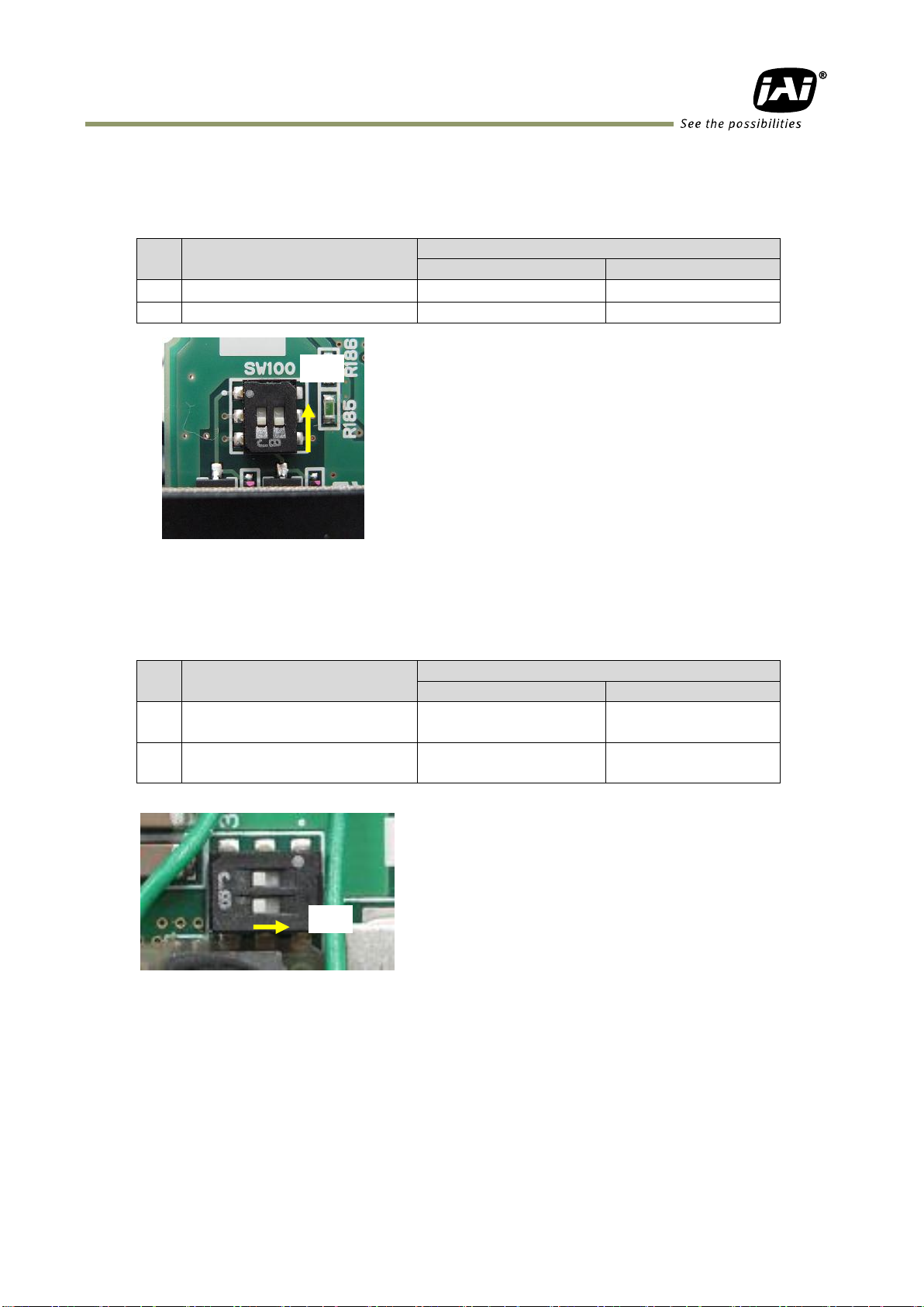
5.4.2 SW-100
This switch can select the type of the signal which is output through 12-pin #10. The factory
default is TTL (XEEN) and it can be changed to Open collector (EEN).
Fig.7. SW100 (Right board looking from the front)
5.4.3 SW-700
This DIP switch can select OPT IN or Iris video output through pin#3 and #4 of the
HIROSE 12 pin connector.
Fig.8 SW700 (On the top board)
- 12 -
Page 15
AT-140GE
DAC
Iris Video
2K2
1K
1μ
0.1μ
+5V
+5V
●
●
●
●
●
SW600
TTL
1K
100K
0.001μ
0.1μ
1K2
15K
39K
75
HIROSE 12P
#10
+5V
1K
0.1
10K
10
10
220
EEN
HIROSE
#9
120
150
Open
Collector
Push
Pull
10K
1K
180
SW100
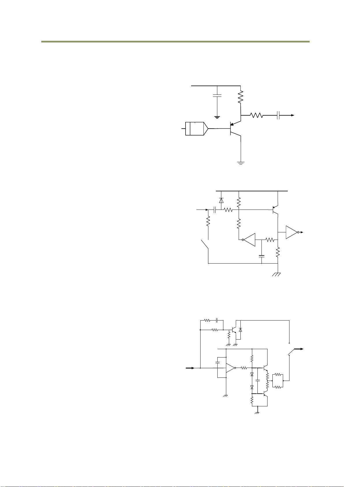
6. Input and output circuits
This chapter introduces the basic diagram and bit allocation of digital output.
6.1. Iris video output
This signal can be used for lens iris control In
Continuous and RCT modes. The signal is NUM
luminance signal and passes through the gain
circuit. However, due to reversed
compensation applied, the gain settings do
not influence this signal. The iris video output
is 0.7 V p-p from 75 and without sync.
Fig. 9 Iris video output.
6.2. Trigger input
The trigger input is on pin #10 on the 12-pin
connector or pin#3 on the D-sub 9-pin
connector. The input is AC coupled. To allow
a long pulse width, the input circuit is a flipflop, which is toggled by the negative or
positive differentiated spikes caused by the
falling or rising trigger edges.
The trigger polarity can be changed.
Trigger input level is 4 V 2 V. It can be
terminated by SW600: ON for 75. OFF for
TTL(Factory default).
Fig.10 Trigger input.
6.3. XEEN output
XEEN is found on pin #4 or #8 on D-sub 9-pin
connector.
The output circuit is 75 complementary
emitter followers. Output level 3 V from 75.
(No termination).
When the open collector is used, the maximum
current is 120mA. However, if a current of more
than 50mA is flowed, it is necessary to use
bigger diameter wires for connecting pin#8 and
9. In case of narrower wires, due to its
resistance, it may not work properly.
This output can be changed to Open collector
signal by SW100.
EEN is found in OPT out in 12-pin connector.
Fig.11 EEN output
- 13 -
Page 16
CCD out
Analog Out
200mV
700mV
230mV↑
800mV
0
100% Level700
200
Analog Out [mV]
CCD Out [mV]
265
930
AT-140GE
6.4. Auto iris video output level
This video output signal is NUM luminance signal and does not have SYNC. It is available only
in Continuous mode and RCT mode. It is also not available in partial scan mode.
This signal is not affected by the gain control.
Fig.12 Iris video output
- 14 -
Page 17
AT-140GE
LUT
( Cross Point Switch )
Pulse Generator 1
(20 bit Counter )
Pulse Generator 0
(20 bit Counter )
12 bit
Counter
TRIGGER 1
TRIGGER 2
TTL OUT 2
OPT OUT 1
OPT OUT 2
Time Stamp Reset
Sequence Reset
LVAL IN
DVAL IN
FVAL IN
EEN IN
OPT IN 1
OPT IN 2
LVDS IN 1
Soft Trigger 0
Soft Trigger 1
Soft Trigger 2
Soft Trigger 3
Pulse trigger IN
Pulse OUT
Pulse Generator 0
Pulse Generator 1
Digital I/O(GPIO) setting
Digital I/O(GPIO) setting
Setting for
Line Source
Setting for
Line Selector
Pixel Clock
Counter Clock Source
1
Counter Divide by value
Bypass0
1 - 4095
Pulse Generator Setting 0
Start Point Counter 0
Length counter 0
Repeat Counter 0
End point counter 0
Counter 0 clear
Pulse Generator Setting 1
Pulse Generator 1
Pulse Generator 0
TTL IN 1
TTL OUT 1
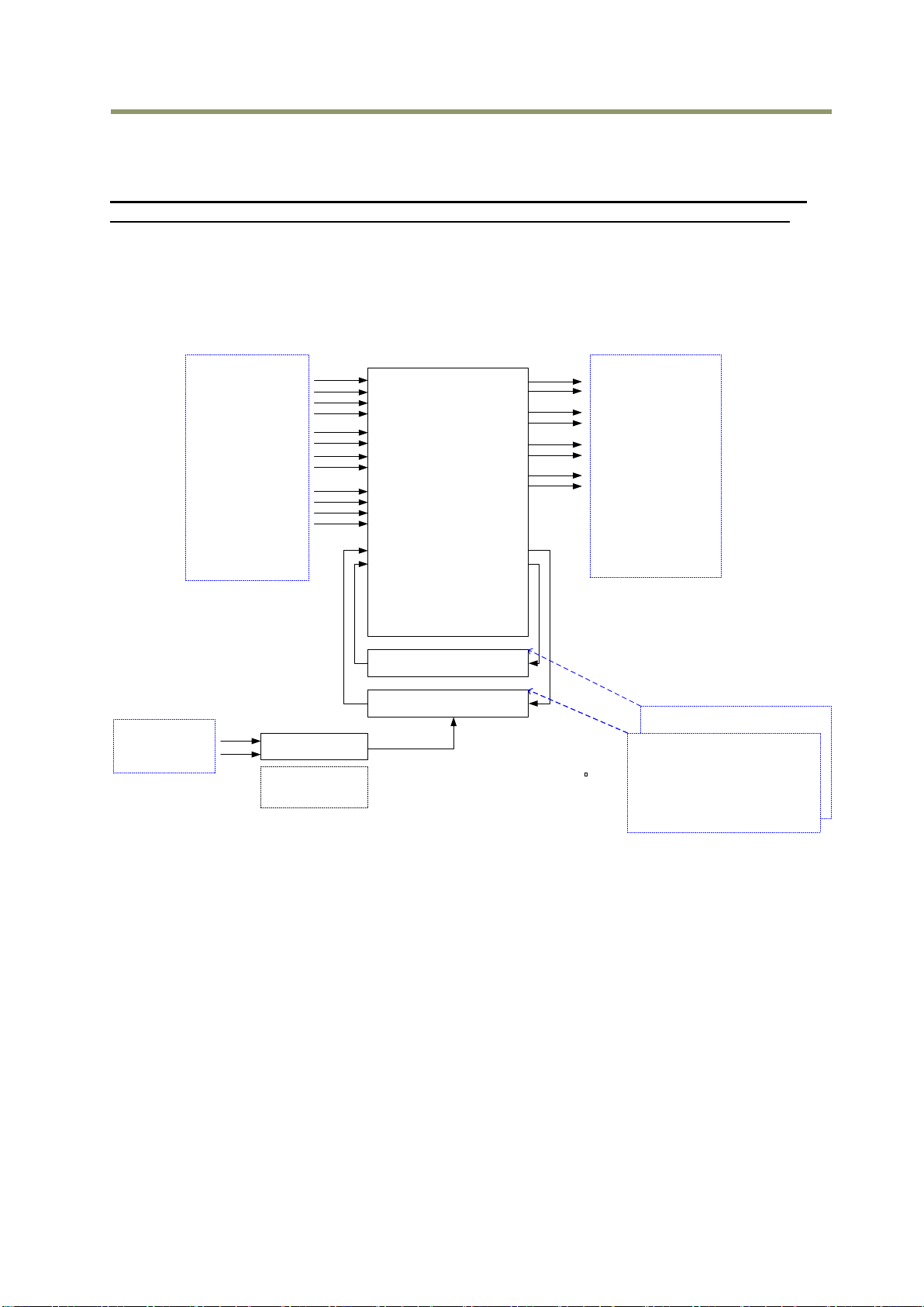
7. GPIO (General purpose inputs and outputs)
In chapter 7, there are some examples of settings. the values shown in these examples
may need to be adjusted to fit the pixel clock specifications of this particular model.
7.1. Overview
All input and output signals pass through the GPIO (General Purpose Input and Output) module.
The GPIO module consists of a Look-Up Table (LUT – Cross-Point Switch), 2 Pulse Generators
and a 12-bit counter. In the LUT, the relationship between inputs, counters and outputs is
governed by internal register set-up.
On the above block diagram, Trigger 0 is used for Exposure and Trigger 1 is used for Delayed
Readout. The Time Stamp Reset can reset the time stamp in compliance with the GigE Vision
standard. This is used for having the same time stamp in case of using multiple cameras.
The blocks shown in the above diagram have the following functionality:
7.1.1 LUT (Look Up Table)
The LUT works as a cross-point switch, which allows connecting inputs and outputs freely.
The signals LVAL_IN, DVAL_IN, FVAL_IN and EEN_IN all originate from the camera timing
circuit. Trigger 0 is connected to the camera's timing circuit and is used for initiating
triggered exposure. Trigger 1 is used for Delayed Readout mode. The Time Stamp Reset
signal is used to reset the camera's time stamp function, also making it possible to reset and
synchronize the time stamp of multiple cameras.
- 15 -
Page 18
AT-140GE
7.1.2 12-bit Counter
The camera pixel clock (42.954 MHz) can be used as a source. The counter has a “Divide by
N”, where N has the range 1 through 4096, allowing a wide range of clock frequencies to be
programmed. Setting value 0 is bypass, setting value 1 is 1/2 dividing and setting value 4095
is 1/4096 dividing.
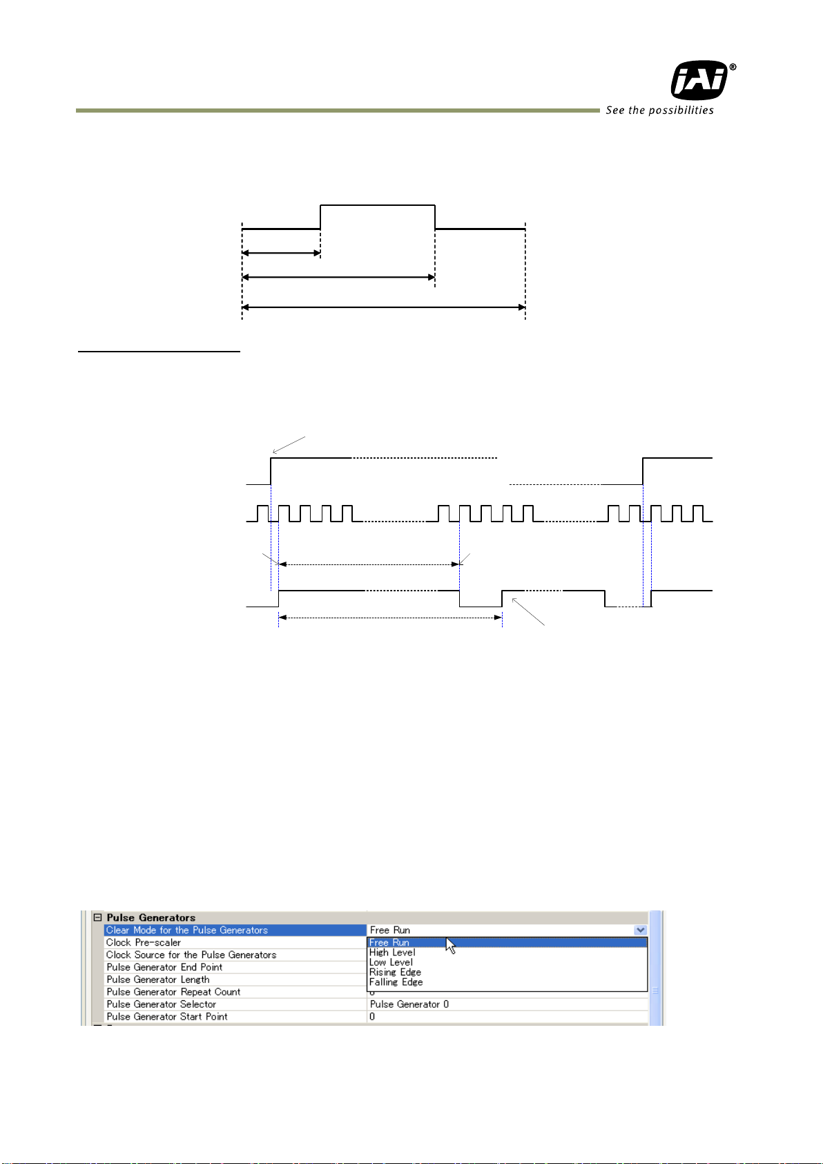
7.1.3 Pulse Generators (0 to 1)
Each pulse generator consists of a 20-bit counter. The behavior of these signals is defined by
their pulse width, start point, end point and number of repetitions.
The pulse generator signals can be set in either triggered or periodic mode.
In triggered mode, the pulse is triggered by the rising edge/falling edge/high level or low
level of the input signal.
In periodic mode, the trigger continuously generates a signal that is based on the configured
pulse width, starting point and end point.
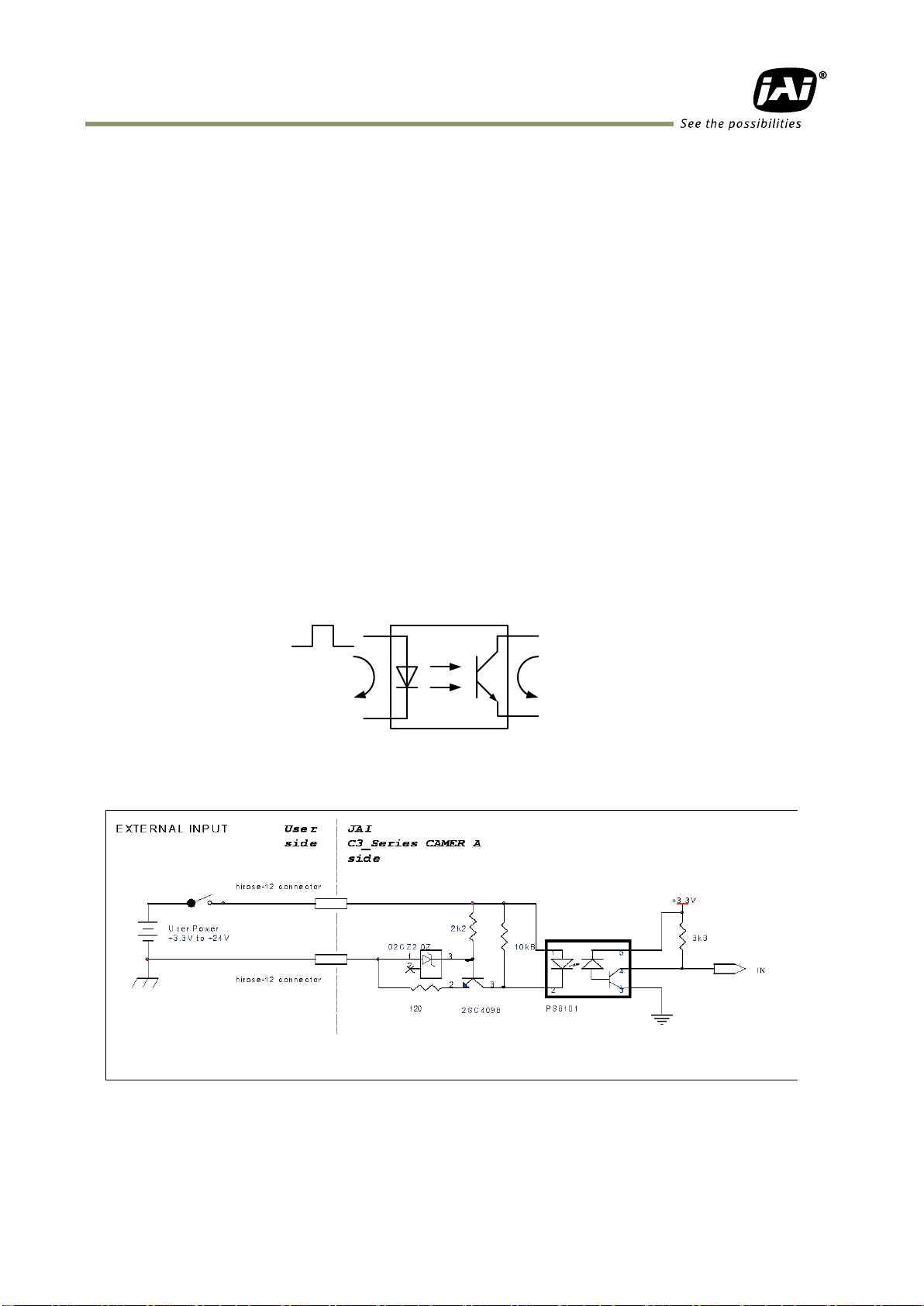
7.2. Opto-isolated Inputs/Outputs
The control interface of the C3 GigE Vision camera series has opto-isolated inputs and outputs,
providing galvanic separation between the camera's inputs/outputs and peripheral equipment.
In addition to galvanic separation, the opto-isolated inputs and outputs can cope with a wide
range of voltages; the voltage range for inputs is +3.3V to +24V DC whereas outputs will
handle +5V to +24V DC.
The figure below shows the functional principle (opto-coupler) of the opto-isolated
inputs/outputs.
Fig.13 Opto-coupler
7.2.1 Recommended External Input circuit diagram for customer
Fig.14 External Input Circuit, OPT IN 1 and 2
- 16 -
Page 19
AT-140GE
User Power (VCC)
3.3V
5V
12V
24V
Time Delay Rising TDR(µs)
0.54
0.54
0.62
0.68
Rising Time RT(µs)
1.2
1.2
2.0
3.0
Falling Delay Time FDR(µs)
1.5
1.5
2.4
2.1
Falling Time FT(µs)
3.6
3.4
4.5
6.8
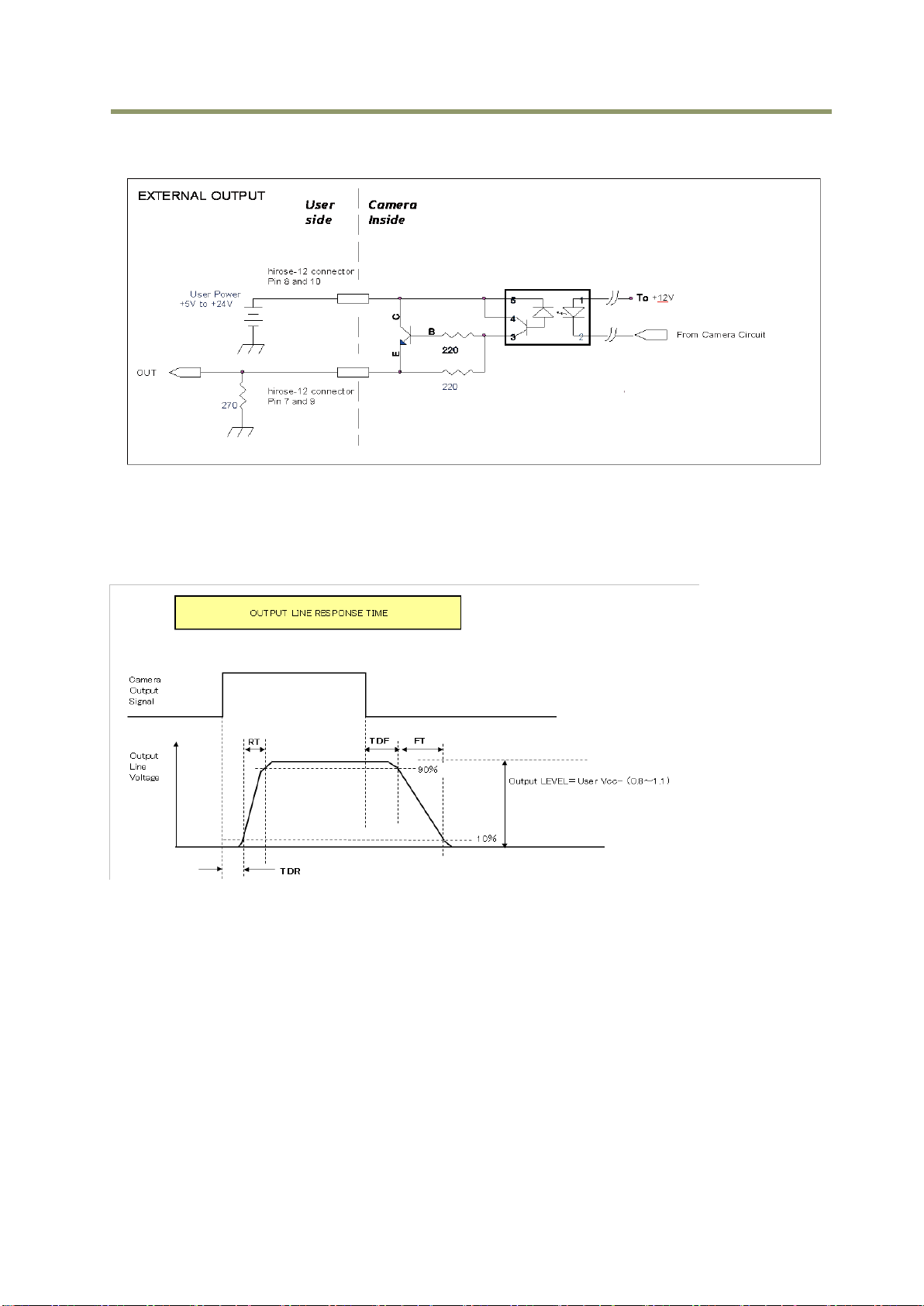
7.2.2 Recommended External Output circuit diagram for customer
Fig.15. External Output Circuit, OPT OUT 1 and 2
7.2.3 Optical Interface Specifications
The relation of the input signal and the output signal through the optical interface is as
follows.
Fig.16 Optical Interface Performance
- 17 -
Page 20
7.3. Inputs and outputs table
Output Port
Trigger
0
Trigger
1
OPT
OUT1
OPT
OUT2
TTL
OUT 1
TTL
OUT 2
Time
Stamp
Reset
Seq.
Reset
Pulse
Gen. 0
Pulse
Gen. 1
Input Port
LVAL IN
× × ×
×
○
○
× ○
○
DVAL IN
× × ×
×
○
○
× ○
○
FVAL IN
× × ×
×
○
○
× ○
○
EEN IN
× × ○
○
○
○
× ○
○
OPT IN 1
○ ○ ○
○
○
○
○ ○ ○
○
OPT IN 2
○ ○ ○
○
○
○
○ ○ ○
○
TTL IN
○ ○ ○
○
○
○
○ ○ ○
○
LVDS IN
○ ○ ○
○
○
○
○ ○ ○
○
Soft Trigger 0
○ ○ ○
○
○
○
○ ○ ○
○
Soft Trigger 1
○ ○ ○
○
○
○
○ ○ ○
○
Soft Trigger 2
○ ○ ○
○
○
○
○ ○ ○
○
Soft Trigger 3
○ ○ ○
○
○
○
○ ○ ○
○
Pulse Gen. 0
○ ○ ○
○
○
○
○ ○ ×
○
Pulse Gen. 1
○ ○ ○
○
○
○
○ ○ ○
×
AT-140GE
LEGEND: 0 = valid combination / x = Not valid (do not use this combination)
- 18 -
Page 21
AT-140GE
Address
Internal Name
GenIcam Name
Access
Size
Value (Range)
0xB004
Counter Dividing Value
ClockPreScaler
R/W
4
0x000: Bypass
0x001: 1/2 Dividing
0x002: 1/3 Dividing
|
0xFFF: 1/4096 Dividing
7.4. Configuring the GPIO module (register settings)
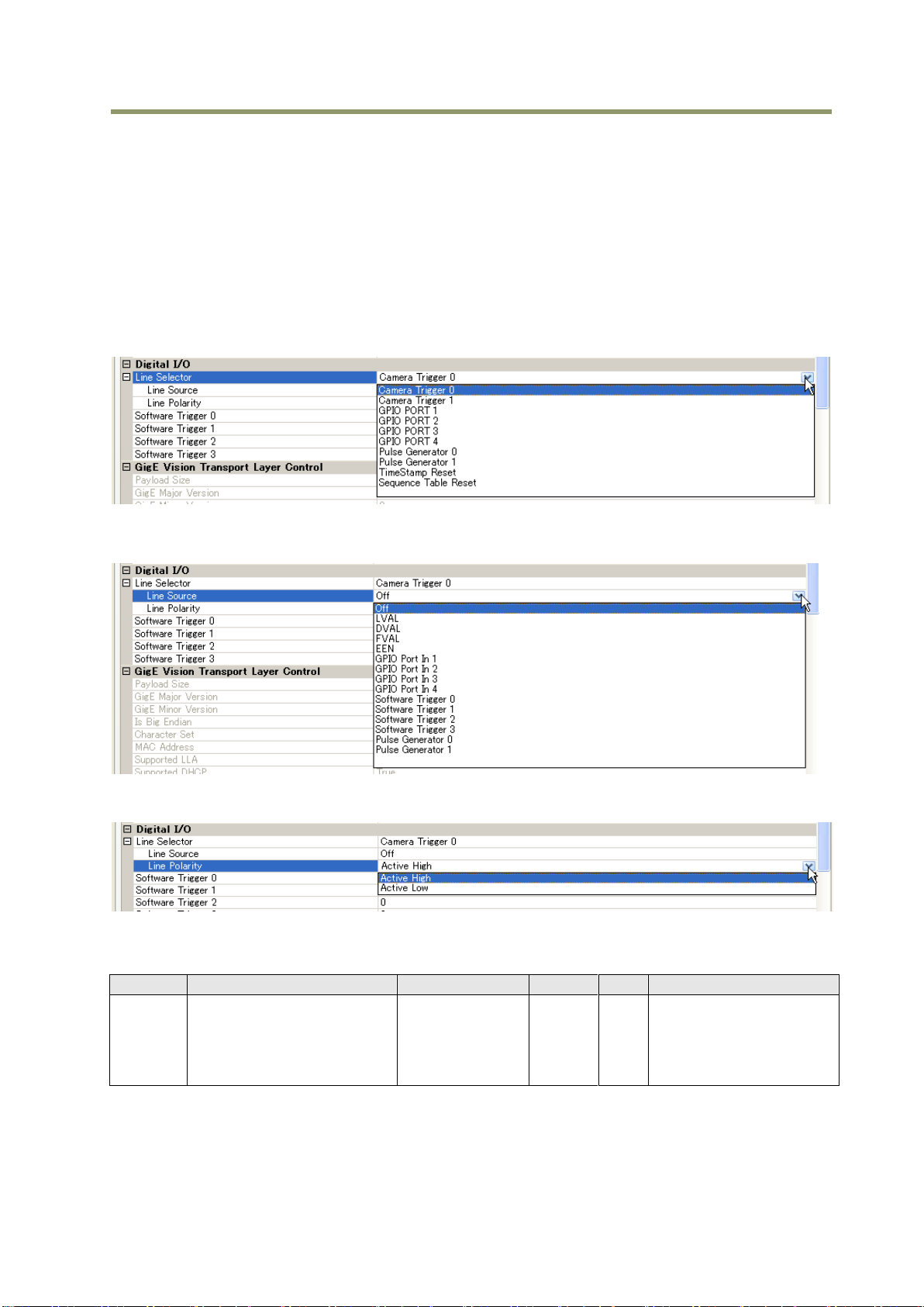
7.4.1 Input /Output Signal Selector
GPIO is used to determine which signal is assigned which terminal. For the details, please
refer to Register Map, Digital I/O, Acquisition and Trigger Control and Pulse Generator.
Line Selector
Line Source
Line Polarity
7.4.2 12-bit counter
- 19 -
Page 22
AT-140GE
Start Point
End Point
Length
Start Point
End Point
Length
Pulse Generator 0 IN
(FVAL )
0 1 2 3
1
99 100 101 102 103
2 1
Start Point = 0 End Point = 99
Length = 102
Clock IN
Clock Source=Pixel Clock ( 60MHz)
Clock Pre-scaler = 2399 ⇒ 25KHz
1/25KHz = 40µs
Pulse Generator Clear = 4: Rising Edge
Pulse Generator 0 OUT
(GPIO Port 1 )
Repeat counter: 0 to 255
=0: Continuously repeated
Pulse Generator Setting Example
7.4.3 Pulse generators (20-bit x 2)
There are 2 pulse generators (designated 0 through 1) that can be used to create various
timing scenarios by programming start point, endpoint, length and repeats.
An example of settings
The following example shows the FVAL input to a pulse generator. The pulse generator
creates the pulse using FVAL and the pulse is output through GPIO PORT 1.
The created pulse rises up at the start point and falls down at the end point, as shown above.
Accordingly, the High duration is (End point – Start point) clocks x (1/Pulse gen. frequency).
In the above example, the original oscillation uses pixel clock (60 MHz) and the pixel clock is
divided by 2400. A pulse frequency of the generator is 25 KHz (60000000/2400). As the start
point is 0 and the end point is 99, a pulse having a width of 100 x 1/25000 = 4ms is created.
If the High duration needs to be delayed against an incoming trigger, the start point should be
set at “N”. The delay value is N x (1/ 25000). In the above example, the N is “0” which is no
delay. The length, in this case, is 102 clocks.
These settings can be achieved by using the JAI Control Tool which is part of the JAI SDK.
Fig.17 Pulse generator setting example
- 20 -
Page 23

7.5. GPIO programming examples
Address
Register
Value
0xA040
Trigger Mode
2 = PWC ( Pulse Width Control)
①
0xB090
Pulse Generator 0 Selector
4 =OPT IN 1
②
0xB000
Clock Choice
1 = Pixel Clock (43MHz)
0xB004
Counter Dividing Value
0 = Pass through
0xB008
Length Counter 0
1000 Clocks
0xB00C
Start point Counter 0
100 Clocks
0xB010
Repeat Count 0
1
0xB014
End point Counter 0
530 Clocks
0xB018
Counter Clear 0
4 = Rising Edge Clear
③
0xB060
CAMERA TRIGGER Selector
16 = pulse generator 0
LUT
( Cross Point Switch )
Pulse Generator 1
(20 bit Counter )
Pulse Generator 0
(20 bit Counter )
12 bit
Counter
TRIGGER 1
TRIGGER 2
TTL OUT 2
OPT OUT 1
OPT OUT 2
Time Stamp Reset
Sequence Reset
LVAL IN
DVAL IN
FVAL IN
EEN IN
OPT IN 1
OPT IN 2
LVDS IN
Soft Trigger 0
Soft Trigger 1
Soft Trigger 2
Soft Trigger 3
Pulse trigger IN
Pulse OUT
Pulse Generator 0
Pulse Generator 1
Digital I/O(GPIO) setting
Digital I/O(GPIO) setting
Setting for
Line Source
Setting for
Line Selector
Pixel Clock
Counter Clock Source
1
Counter Divide by value
Bypass0
1 - 4095
Pulse Generator Setting 0
Start Point Counter 0
Length counter 0
Repeat Count 0
End point counter 0
Counter 0 clear
Pulse Generator Setting 3
Pulse Generator 1
Pulse Generator 0
TTL IN
①
②
⇒
⇒
⇒
⇒
⇒
1000clk
100clk
1
530clk
4 Rising Edge
③
TTL OUT 1
OPT IN
PULSE Generator 0
OUT
100
530
1000
7.5.1 GPIO Plus PWC shutter
Example: 10µs unit pulse width exposure control (PWC).
Pixel clock is ~43MHz. 430 clocks (530-100) equals 10µs.
AT-140GE
Fig.18 Pulse Generator Timing Example 1
- 21 -
Page 24

Pulse Generator 0
100 Line
500 Line
1000 Line
output
Pulse Generator 0
100 Line
500 Line
1000 Line
output
7.5.2 Internal Trigger Generator
Address
Register
Value
0xA040
Trigger Mode
1 = EPS
①
0xB000
Clock Choice
1 = Pixel Clock
0xB004
Counter Dividing Value
1829= 1/1830 dev(Line Rate)
0xB008
Length Counter 0
1000 Clocks
0xB00C
Start point Counter 0
100 Clocks
0xB010
Repeat Count 0
0 = Free Run
0xB014
End point Counter 0
500 Clocks
0xB018
Counter Clear 0
0 = No Clear
②
0xB060
CAMERA TRIGGER Selector
11 = pulse generator 0
LUT
( Cross Point Switch )
Pulse Generator 1
(20 bit Counter )
Pulse Generator 0
(20 bit Counter )
12 bit
Counter
TRIGGER 1
TRIGGER 2
TTL OUT 2
OPT OUT 1
OPT OUT 2
Time Stamp Reset
Sequence Reset
LVAL IN
DVAL IN
FVAL IN
EEN IN
OPT IN 1
OPT IN 2
LVDS IN 1
Soft Trigger 0
Soft Trigger 1
Soft Trigger 2
Soft Trigger 3
Pulse trigger IN
Pulse OUT
Pulse Generator 0
Pulse Generator 1
Digital I/O(GPIO) setting
Digital I/O(GPIO) setting
Setting for
Line Source
Setting for
Line Selector
Pixel Clock
Counter Clock Source
1
Counter Divide by value
Bypass0
1 - 4095
Pulse Generator Setting 0
Start Point Counter 0
Length counter 0
Repeat Count 0
End point counter 0
Counter 0 clear
Pulse Generator Setting 3
Pulse Generator 1
Pulse Generator 0
TTL IN 1
①
②
⇒
⇒
⇒
⇒
⇒
1000clk
100clk
0
500clk
0 Free run
TTL OUT 1
Create a trigger signal and trigger the camera
AT-140GE
Fig.19 Pulse Generator 0 timing Example 2
- 22 -
Page 25

AT-140GE
Analog Signal [mV]
Black Level
1023
890
32
0
25
700
Digital Out [LSB]
White Clip Level
100% Level
800
CCD out
Analog Signal *
Digital Out(24-bit)
Digital Out(32-bit)
Black
Setup 3.6%, 25mV
8LSB
32LSB
200mV
700mV
222LSB
890LSB
230mV
800mV
255LSB
1023LSB
0 1 2 3 4 5 6 7 0 1 2 3 4 5 6 7 0 1 2 3 4 5 6 7
R0G0B0
8. GigE Vision Streaming Protocol (GVSP)
8.1. Digital Video Output (Bit Allocation)
Although the AT-140GE is a digital camera, the image is generated by an analog component,
the CCD sensor.
The table and diagram below show the relationship between the analog CCD output level and
the digital output.
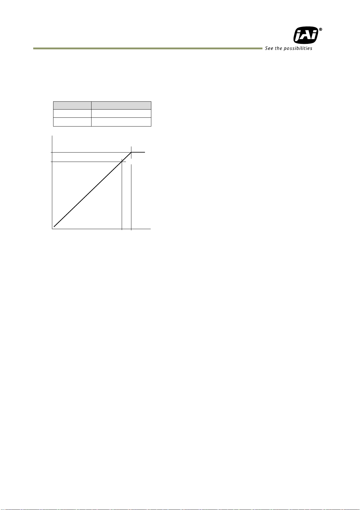
The standard setting for 10-bit video level is 890 LSB. 200 mV CCD output level equals 100%
video output.
Fig.20 Digital output (10-bit output)
8.2. Bit Allocation (Pixel Format / Pixel Type)
In the GigE Vision Interface, GVSP (GigE Vision Streaming Protocol) is used for an application
layer protocol relying on the UDP transport layer protocol. It allows an application to receive
image data, image information and other information from a device.
As for the sensors in the AT-140GE, the following pixel types supported by GVSP are available.
With regard to the details of GVSP, please refer to the GigE Vision Specification available
from the AIA (www.machinevisiononline.org).
8.2.1 GVSP_PIX_RGB8_PACKED (RGB 24bit output)
1 Byte 2 Byte 3 Byte 4 Byte
- 23 -
Page 26

AT-140GE
0 1 0 1 0 1 X X 0 1 2 3 4 5 6 7 0 1 2 3 4 5 6 7 0 1 2 3 4 5 6 7
B0
B0G0R0
R0
G0
0 1 2 3 4 5 6 7 8 9 0 1 2 3 4 5 6 7 8 9 0 1 2 3 4 5 6 7 8 9 X X
R0
B0
G0
Address
Internal Name
Access
Size
Value
0xA410
Pixel Format type
R/W
4
0x02180014:RGB8Packed
0x0220001C:RGB10V1Packed
0x0220001D:RGB10V2Packed
8.2.2 GVSP_PIX_RGB10V1_PACKED (RGB 32bit output)
1 Byte 2 Byte 3 Byte 4 Byte
8.2.3 GVSP_PIX_RGB10V2_PACKED (RGB 32bit output)
1 Byte 2 Byte 3 Byte 4 Byte
9. Functions and Operations
9.1. GigE Vision Standard Interface
The AT-140GE is designed in accordance with the GigE Vision standard. Digital images are
transmitted over Cat5e or Cat6 Ethernet cables. All camera functions are also controlled via
the GigE Vision interface.
The camera can operate in Continuous mode, providing an endless stream of images. For
capturing individual images related to a specific event, the camera can also be triggered. For
precise triggering, it is recommended to use a hardware trigger applied to the Hirose 12-pin
connector. It is also possible to initiate a software trigger through the GigE Vision interface.
However, when using a software trigger, certain latency inherent to the GigE interface must
be expected. This latency, which manifests itself as jitter, greatly depends on the general
conditions and traffic on the GigE connection. The frame rate described in this manual is for
the ideal case and may deteriorate depending on conditions.
When using multiple cameras (going through a switch and/or a single path) or when operating
in a system with limited transmission bandwidth the Delayed Readout Mode and Inter-Packet
Delay functions can be useful.
9.2. Recommended Network Configurations
Although the AT-140GE conforms to Gigabit Ethernet (IEEE 802.3) not all combinations of
network interface cards (NICs) and switches/routers are suitable for use with the GigE Vision
compliant camera.
JAI will endeavor to continuously verify these combinations, in order to give users the widest
choice of GigE components for their system design.
- 24 -
Page 27

AT-140GE
Model
Pixel Type
Frame Rate
Packet data volume
(assumes the packet size is 4036)
AT-140GE
RGB8Packed
20.77 fps
732 Mbit/s
RGB10V1Packed
RGB10V2Packed
20.77 fps
(Note 1)
972 Mbit/s
9.2.1 Guideline for network settings
To ensure the integrity of packets transmitted from the camera, it is recommended to follow
these simple guidelines:
1. Whenever possible use a peer-to-peer network.
2. When connecting several cameras going through a network switch, make sure it is
capable of handling jumbo packets and that it has sufficient memory capacity.
3. Configure inter-packet delay to avoid congestion in network switches.
4. Disable screen saver and power save functions on computers.
5. Use high performance computers with multi-CPU, hyper-thread and 64-bit CPU, etc.
6. Only use Gigabit Ethernet equipment and components together with the camera.
7. Use at least Cat5e and preferably Cat6 Ethernet cables.
8. Whenever possible, limit the camera output to 8-bit.
☞ For more details regarding network settings, please refer to the “Getting Started Guide” which
is a separate document.
9.2.2 Video data rate (network bandwidth)
The video bit rate for the AT-140GE in Continuous mode is:
Note1: depending on the packet size, the frame rate of 20.77 fps may not be achieved. It
may be reduced to 18 to 19 frames per seconds. This figure will depend of the system
configuration used (RESEND not possible)
If Jumbo Frames (Max.16020) are not used, the packet data will be bigger by 2%.
If Jumbo frames are used, the packet size may be automatically optimized to a smaller size.
For details of setting Jumbo Frames, please refer to the “Getting Started Guide”.
9.2.3 Note for setting packet size
The packet size is set to 1476 as the factory default. Users may enter any value for the
packet size and the value will be internally adjusted to an appropriate, legal value that
complies with the GenICam standard. The packet size can be modified in the GigE Vision
Transport Layer Control section of the camera control tool.
Regarding data transfer rate, a larger packet size produces a slightly lower data transfer
rate. The AT-140GE can support a maximum of 16020 byte packets provided the NIC being
used has a Jumbo Frames function with a setting of a 16020 bytes or larger.
Caution: do not set the packet size larger than the maximum setting available in the
NIC or switch to which the camera is connected . Doing so will cause output
to be blocked.
- 25 -
Page 28

AT-140GE
Item
Unit
Symbol
Image Width
[pixels]
A
Image Height
[pixels]
B
Bits per Pixel
[bits]
C
Frame Rate
[fps]
D
Packet Size
[Bytes]
E
Number of Packets (including Data Leader & Trailer
Packet)
[packets]
G
Data Transfer Rate
[Mbit/s]
J
Item
Unit
value
Data Leader Packet Size
[Bytes]
90
Data Trailer Packet Size
[Bytes]
62
J={90+62+(E+18)*(G-2)}*8*D/1000000
Where, G=ROUNDUP{A*B*C/8/(E-36)}+2
Pixel format
Bit
RGB8
24
RGB10V1Packed
32
RGB10V2Packed
32
Item
Unit
Symbol
Setting
Image Width
[pixels]
A
1392
Image Height
[pixels]
B
1040
Bits per Pixel
[bits] C 24
Frame Rate
[fps]
D
20.77
Packet Size
[Bytes]
E
4036
Number of Packets (including Data Leader & Trailer
Packet)
[packets]
G
Transfer Data Rate
[Mbit/s]
J
9.2.4 Calculation of Data Transfer Rate
In order to calculate the data transfer rate, the following parameters and formula are
required.
Setting parameter
Fixed value
Formula to calculate Data Transfer Rate
The following table shows Bits per Pixel (Item C) which depends on the pixel format.
Calculation example: AT-140GE Pixel type RGB8
G=ROUNDUP {(1392 x 1024 x 24/ 8 / (4036-36)) + 2 = 1086 + 2 = 1088
J={90+62+(4036+18)x(1088-2)} x 8 x 20.77 / 1000000 = 732 Mbit/s
- 26 -
Page 29

AT-140GE
Pixel Type
Frame rate at Full Frame scan[fps]
RGB8_Packed
Approx. 2
RGB10V1_Packed,RGB10V2_Packed
Approx.1.5
750 nm700650600550
50
0
450
4
0
0
Light
CCD
CCD
CCD
B ch
A/D & process circuit
Blemish compensation
Shading compensation
Color matrix
LUT/Gamma/Knee
GigE Interface
G ch
A/D & process circuit
Blemish compensation
Shading compensation
Color matrix
LUT/Gamma/Knee
R ch
A/D & process circuit
Blemish compensation
Shading compensation
Color matrix
LUT/Gamma/Knee
750 nm700650600550
50
0
450
4
0
0
750 nm700650600550
50
0
450
4
0
0
9.2.5 Note for 100BASE-TX connection
In order to use 100Mbps network, 100BASE-TX and Full Duplex are available. Half
Duplex cannot be used.
In the case of connecting on 100BASE-TX, the maximum packet size should be 1500
bytes.
In the case the of connecting on 100BASE-TX, the specifications such as frame rate,
trigger interval and so on described in this manual cannot be satisfied.
Note: The above frame rates are based on approx. 70Mbps of total frame transfer data.
9.3. Basic Functions
9.3.1 Basic construction
The AT-140GE is a 3CCD camera equipped with F4, 1/2 inch prism optics. Red, green and blue
color signals are taken from each 1.45 mega CCD which are filtered to the red, green and
blue spectral wavelengths. A 32-bit microprocessor controls all functions in the AT-140GE
camera. The CCD sensor output is normalized in CDS and preamplifiers. The signals are then
digitized to 16 bits. Digital gain control, color matrix, look-up tables and setup can do signal
processing in 16 bits before the signal is converted to a 32- or 24-bit RGB pixel format via
GigE Vision interface.
Fig.21 Principle diagram for signal processing
- 27 -
Page 30

AT-140GE
Fast-dump period
Fast-dump period
Normal scan period
9.3.2 Modes of operation
The AT-140GE has multiple operating modes including a normal continuous mode, triggered
modes and others. In the normal continuous mode, the camera runs at 20.77 frames per
second continuously. This is used for operation when a trigger signal is not required. There
are 5 triggered modes and the trigger signal is supplied via HIROSE 12-pin or D-Sub 9-pin
connectors. In the triggered modes, the frame rate is 20 fps.
Normal continuous mode
Edge pre-select trigger mode (EPS)
Pulse width control trigger mode (PWC)
Reset continuous trigger mode (RCT)
EPS Sequential trigger mode
Frame delay readout trigger mode (EPS and PWC)
Smearless mode
OB transfer mode
Multi ROI mode
9.3.3 Partial scan (Fast Dump ON)
The partial scanning function uses the middle of the image vertically to achieve faster frame
rates. This is very useful when capturing and inspecting an image which does not require the
full height.
Full scan Partial Scan
Fig.22 Partial scan conceptual drawing
The partial scan mode for the AT-140GE is variable. The first line and the last line to be read
out can be set.
The variable scan readout is connected with the ROI settings.
1. If ROI is set, these settings are applied to the partial scan settings.
2. If the multi ROI feature is used, the smallest line number and the largest line number of
the multi ROI areas define the partial scan area.
3. When the sequence trigger is used, the situation is the same as for multi ROI. The smallest
line and the largest line define the partial scan.
In order to execute partial scanning, the fast dump setting should be ON.
The first line can be set anywhere from the 1st line to 1033rd line and the end line can be set
from the 8th line to 1040th line. This means the minimum height of the partial scan is 8 lines.
- 28 -
Page 31

AT-140GE
Image Height
Image start line
/ end line
Minimum: 8 line Maximum: 1040 lines
Image starts at 1st line
Image starts at 1033rd line
This is in case image height is 8 line
1/8
1033
/1040
8 line
1040 lines
Fig.23 Variable Partial scan
How to calculate total line number and frame rate in variable partial scan mode
Frame rate (fps) = Horizontal frequency(21.938KHz) / Total lines
Total lines = ①OB period + ②Fast Dump period in the upper part of the frame (L) +
③Effective image period (L) + ④Fast dump period in the lower part of frame
(L) + ⑤Blank period (L)
Where,
OB period = 4L (Fixed)
Blank period = 6L (Fixed)
Fast dump period for the upper part = Round up
Fast dump period for the lower part = Roud up
4+Start line 1
1040End line +2
4
4
Calculation example
Readout: 1/2 partial scan at the center (520L), Start line (261), End line (780)
OB period = 4L
Blank period =6L
Fast dump period for the upper part = (4+261-1) ÷4 +1= 66 + 1=67 67
Fast dump period for the lower part = (1040-780+2) ÷ 4 =65.5 66
Total lines = 4+67+520+66 +6 = 663
Frame rate = 21.938/ 663 =33.08 fps
+ 1
- 29 -
Page 32

AT-140GE
Setting
Effective/total
Horizontal
Frequency
Frame rate
Off (No V Binning))
1040 /1056
21.938 KHz
20.77 frames/sec.
2:1 V Binning
520 / 530
17.447 KHz
32.92 frames /sec.
Mode
Read Out
Minimum shutter speed
Maximum
shutter speed
Continuous
Edge Pre-select
Full
Partial
22.8 µs at PE=0(1/43,000s)
45.58µs x
1056L=1 Frame
(48.13 ms)
V binning
28.7 μs at PE=0(1/35,000s)
Pulse Width
Full
Partial
45.58 µs x 2L+22.9 µs( 0.5L)=
114 µs (≒1/10,000s)(Note)
42 Frames
( 2 seconds )
V Binning
57.32 µs x 2L + 28.7 µs(0.5L)=
143.3µs (≒1/8.000s)(Note)
Note: In Pulse Width mode, the minimum trigger pulse width requires more than 2LVAL.
Horizontal Direction
Vertical Direction
Full
Full
1/2
Binning
Frame rate 25.21 fps
Frame rate 40.98 fps
Normal full scanning
2 line Vertical Binning
H
H
Horizontal CCD Register
S/H
Reset
Video
Out
Xsg1
Vertical CCD Register
Pixel
9.3.4 Vertical Binning (VB)
Vertical Binning mode is a function where the signal charges from 2 adjacent (vertical) pixels
are added together and read out as one pixel. Binning results in half vertical resolution but
higher frame rate and sensitivity. The charge accumulated in 2 adjacent lines is added
together in the horizontal CCD register. This is done by providing two pulses to the vertical
CCD register for each line read out. Vertical binning cannot be used together with partial
scanning.
Fig.24 Vertical Binning
9.3.5 Electronic shutter (SM)
The AT-140GE has the following shutter modes.
Programmable Exposure (PE)
The setting command is PE and the exposure time can be controlled from 0L to 1056L in 1
LVAL units (45.58µs). Calculating actual shutter speed requires adding 0.5L to the
setting value. This is because there is 0.5L overhead.
The resulting range is from 0.5LVAL to 1056LVAL. Setting 1056L is Shutter OFF.
Programmable exposure can be set for R, G and B together or individually in EPS and RCT
modes.
The shutter speed for each operation mode is shown below.
- 30 -
Page 33

AT-140GE
FVAL
(1)
(3)
(1) In this period camera executes trigger at next LVAL (prevents feed-through noise)
(2) Avoid trigger at FVAL transition (+/- LVAL period), as the function may randomly
switch between “ next LVAL ” and “ immediate ”.
(2)
External Trigger
+/- 1 LVAL
(3)
In this period, camera executes trigger immediately ( no delay).
Exposure Time Abs (GenICam
Standard)
This is a function specified in the GenICam standard.
The shutter speed can be entered as an absolute exposure time in microseconds (μs) in
register address 0xA018. The entered absolute time (Time Abs) is then converted to a
programmable exposure (PE) value inside the camera.
The calculating formula below shows the relationship between the PE value used by the
camera for the different readout modes and the value entered in register 0xA018.
Due to rounding (decimals rounded down), some discrepancies may occur.
The relation between PE value and Time Abs
Normal readout PE= INT (Exposure time – 64.13) µs / (1958/42954000)
Vertical Binning PE= INT (Exposure time – 84.13) µs / (2462/42954000)
(Note: INT means round down.)
Note :The minimum value in normal readout is 22.8µs.
GPIO in combination with Pulse Width trigger
More precise exposure time can be obtained by using GPIO in combination with Pulse Width
mode. The clock generator and counter can be programmed in very fine increments.
For an example, refer to 7.5.1 GPIO Plus PWC shutter
Auto shutter
The AT-140GE has an automatic shutter function which sets the video at an appropriate level
depending on illumination.
Auto shutter range : 1/25 sec to 1/250 sec
9.3.6 Auto-detect LVAL-sync / async accumulation
This function replaces the manual setting found in older JAI cameras. Whether accumulation
is synchronous or asynchronous in relation to LVAL depends on the timing of the trigger input.
When a trigger is received while FVAL is high (during readout), the camera works in LVALsynchronous mode, preventing reset feed-through in the video signal. There is a maximum
jitter of one LVAL period from issuing a trigger and accumulation start.
When a trigger is received during FVAL low, the camera works in LVAL-asynchronous mode (no
delay) mode.
This applies to both Edge Pre-select (EPS) trigger mode and Pulse Width Control (PWC) trigger
mode.
Fig.25 Auto-detect LVAL sync/async accumulation
- 31 -
Page 34

AT-140GE
Video Level
Video Level
Video Level
Video Level
Fig.26 Shading compensation
9.4. Pre-processing functions
9.4.1 Shading compensation
The AT-140GE implements a digital shading compensation
circuit for the white shading which could be caused in the
prism or optical system. The whole image is divided
horizontally and vertically and uses the center level as the
reference. The circuit will compensate the difference between
the center and each divided area. The range for compensation
is a maximum of 30%. In the factory, the shading compensation
is done under the following conditions and stored in the
“Factory” area of the memory.
Lens used: Kowa 12mm F1.8 to F16
F value: F5.6
Note: Conditions for lens used with AT-140GE
In order to get an appropriate picture, it is recommended to use 1/2 inch, 3CCD lenses.
Shading is dependent on F value and focal length. Using a wide angle lens or using the
lens fully open, will cause the shading characteristics to deteriorate.
The AT-140GE has two shading compensation circuits.
1. Color shading compensation
In this mode, the shading is compensated using the G channel as the reference.
Adjust R and B channels to match the characteristics of the G channel. Use white balance
to match R, G and B levels.
Fig.27 Conceptual drawing for color shading compensation
2. Flat shading compensation
In this mode, each channel can be adjusted to achieve flat characteristics.
Fig.28 Conceptual drawing for flat shading compensation
- 32 -
Page 35

AT-140GE
Continuous
One push
Manual
Tracking range
4000K to 9,000K
4000K to 9,000K
4000K to 9,000K
Adjustable range
-6dB ~ +6dB
-6dB ~ +6dB
-6dB ~ +6dB
Store the setting value
No
Yes
Yes
8
8
Windousize X :2
Window size Y :2
Window offset X :3
Window offset Y : 3
Setting example
Fig.29 White balance measuring area
9.4.2 White balance
The AT-140GE has 4 white balance modes: manual balance, one push auto white balance,
continuous auto white balance and pre-set white balance.
The pre-set white balance can be set to 4000K, 4600K or 5600K.
The white balance of the AT-140GE is set under 7800K lighting in factory. When the camera is
started up at the first time, it is white balanced to 7800K and R and B gain settings are 0.
For executing the white balance, the entire image is
divided into 64 areas, 8 for horizontal and 8 for vertical.
The following drawing is an example of using a 2 x 2 area in the image center.
Note: In continuous mode, if the white part is not enough to make an adjustment, the white balance
may not achieve a proper white color.
Note: The completion of one push auto white requires a maximum of 5 seconds to complete.
Note: If the master gain is set less than 0dB, R and B gain can not be controlled up to -6dB. For
instance, if the master gain is set at -3dB, the saturation level of R and B gain is deteriorated
under 0dB.
9.4.3 Linear matrix
The AT-140GE incorporates a linear color matrix circuit to improve color reproduction.
As this circuit processes signals in the linear stage, before the gamma correction circuit, the
gamma circuit does not affect color reproduction.
This circuit has:
1. Linear OFF
2. sRGB Standard which HP and Microsoft specify for printers and monitors. This preset
is based on this standard.
3. Adobe RGB Standard which Adobe systems specify. This preset is based on this standard.
4. User User can manipulate R, G and B color relationships based on applications. Set
the gain for R-R, R-G, R-B, G-R, G-G, G-B, B-R, B-G, B-B to adjust.
Important Note:
If sRGB or Adobe RGB is used, please note the following procedure.
1) Achieve the white balance under the condition of D65 (6500K) illumination.
2) Gamma should be set at 0.45 and set the linear matrix at either sRGB or Adobe RGB.
3) Monitor should comply with sRGB or Adobe RGB color reproduction capability.
- 33 -
Page 36

AT-140GE
CCD out
Analog Signal
Digital Out(32bit)
Digital Out(24bit)
Black
Setup 3.6%, 25mV
32LSB
8LSB
200mV
700mV
890LSB
222LSB
230mV↑
800mV
1023LSB
255LSB
Functions
Data length
Setting range
Knee Point
10bit
0LSB ~ 1023LSB
Knee Slope
12bit
0(x0.0005) ~ 4095(x2.0000)
Defective Pixel
Video Input
Video Output
Knee Slope
Knee Point
Analog Signal [mV]
Black Level
1023
890
32
0
25
700
Digital Out [LSB]
100% Level
White Clip Level
835
9.4.4 Blemish compensation
The AT-140GE has a blemish compensation circuit.
Blemish control has 0:OFF, 1:Black, 2:White and 3:Both. When 1, 2 or 3 is selected, the
stored factory data can be loaded.
Fig.30 Conceptual drawing for blemish compensation
9.4.5 Gamma setting (Look Up Table)
The AT-140GE has various gamma settings
including LUT (Look Up Table). Gamma can be
set OFF (1.0), 0.6, 0.45, or to exhibit
characteristics set using LUT.
The following shows the typical characteristics
in the case of gamma 0.6.
Fig.31. Gamma setting
9.4.6 Knee compensation
If the relation of input and output is linear (1:1), the
output signal is saturated at a certain level of the
input signal and details cannot be reproduced in the
saturated area. The knee compensation circuit
maintains linear output up to a knee point and
compresses the level after the knee point. This is set
by a knee slope function. The AT-140GE supports up
to 200% signal compression by knee slope. Factory
default is OFF.
Fig.32 Example of Knee characteristics
- 34 -
Page 37

AT-140GE
Value
Description
0
OFF
4
Horizopntal Ramp Scale
5
Vertical Ramp Scale
6
Moving Ramp Scale
8
Normal Color Bar
9
Vertical Color Bar
10
Moving Color Bar
1 = Vertical 2 = Horizontal 3 = Both
9.5. Other functions
9.5.1 Test pattern generator (Address 0xA13C)
The AT-140GE has an internal test pattern generator. These signals are output as the last
process of the digital signal processing circuit and can be used for adjustment of the related
system. The AT-140GE has a total of 6 test pattern types.
9.5.2 Center marker
The AT-140GE is equipped with a center marker generator. The center marker can be
selected from three types as described below.
Note: The center marker is displayed only in full scan mode.
Fig.33 Center marker
- 35 -
Page 38

9.6. Sensor Layout and timing
blank
Read Out
(Vertical)
1050
Active Pixels
1392(H)x1040(V)
Optical Black Lines
Optical Black
1392
2
4
8
2
blank
1958 Clock
Read Out (Horizontal)
6
524
1434
1040
1056
9.6.1 CCD Sensor Layout
Fig.34 CCD sensor layout
AT-140GE
- 36 -
Page 39

AT-140GE
D A TA O U T
D V AL
C CD Ou t
F VA L
S UB
S G
E E N
L V A L
X E E N
(Hi rose 12pi n)
Du mmy +
Bl a n k
OB
Re s e r v ed
OB
4 0 c k
Re s e r v ed
2
1 3 9 2 ck
1 4 3 4 ck
1392 ck
1958 ck
1434 ck 524 ck
1 ck=42.954 NHz (23.28 ns/ck)
1866 ck
86 ck
92
945 ck
859 ck
86
167
20 ck
524 ck
524 ck
2 ck
FVAL Rising Edge
FVAL Falling Edge
1 LVAL Period
Effective Pixels
Exposure Period
123
4 5
D A T A O U T
D V A L
L V A L
S U B
S G
F V A L
E E N
FVA L
LVA L
1 F V A L p e r i o d
E x p o s u r e
P e r i o d
X E E N
(Hir ose 12pi n)
10 56 L
10 50 L
6L
1L = 2134Cl ock ( 36. 79us)
8L
OB
R
e
s
e
r
v
e
d
E f f e ct i v e L i n es
10 40 L
Re s er ved
B l a nk
OB
1
0
4
0
1
0
3
9
1
0
3
8
1
0
3
7
1
0
3
6
6L
2
0.5L
9.6.2. Horizontal timing (Normal continuous mode)
Fig. 35 Horizontal timing
9.6.3 Vertical timing (Normal continuous mode)
Fig.36 Vertical timing for full scan
- 37 -
Page 40

AT-140GE
D A TA O U T
D V AL
C CD Ou t
F VA L
S UB
S G
E E N
L V A L
X E E N
(Hi rose 12pi n)
Du mmy +
Bl a n k
OB
Re s e r v ed
OB
4 0 c k
Re s e r v ed
2
1 3 9 2 ck
1 4 3 4 ck
1392 ck
1958 ck
1434 ck 524 ck
1 ck=42.954 NHz (23.28 ns/ck)
1866 ck
86 ck
92
945 ck
859 ck
86
167
20 ck
524 ck
524 ck
2 ck
FVAL Rising Edge
FVAL Falling Edge
1 LVAL Period
Effective Pixels
Exposure Period
9.6.4 Horizontal timing (Partial scan mode)
Fig.37 Horizontal timing (Partial scan, the same as normal continuous)
9.6.5 Vertical timing (Partial scan mode)
Fig.38 Vertical timing (Example:1/8 partial scan setting)
- 38 -
Page 41

AT-140GE
Partial scan
examples
Effective lines
Total lines
Horizontal
Frequency
Frame rate
2/3
692
792
21.938 KHz
27.69 fps
1/2
520
663
21.938 KHz
33.08 fps
1/4
260
468
21.938 KHz
46.87 fps
1/8
128
369
21.938 KHz
59.45 fps
D A TA O U T
D V AL
C CD Ou t
F VA L
S UB
S G
E E N
L V A L
X E E N
(Hi rose 12pi n)
Du mmy +
Bl a n k
OB
1 4 3 4
1 3 9 2
1 3 9 2
1 4 3 4
OB
2
9
c k
4
0 c k
2 9 c k
467
2462
1028
1 clock =42.954 MHz (23.28ns/Clock)
86
92
2370
86
1289(30μs)
1375
1028
1028
1 LVAL period
FVAL Rising Edge
FVAL Falling Edge
Effective Pixels
Exposure Period
9.6.6 Horizontal timing (Vertical binning mode)
Fig. 39 Horizontal timing for V binning.
- 39 -
Page 42

AT-140GE
9.6.7 Vertical timing (vertical binning mode)
Fig.40 Vertical timing for V binning.
9.7. Operation Modes - Timing
9.7.1 Continuous operation
For applications not requiring asynchronous external triggering, this mode should be used. In
this mode it possible to use a lens with a video controlled iris.
For timing details, refer to fig.35. through fig.40.
To use this mode:
Set function: Exposure mode Continuous
Pixel format RGB8, 10V1, 10V2
Partial scan Fast dump ON, ROI
Vertical binning Binning vertical ON
Shutter mode Programmable, Exposure Time Abs,
Auto shutter
- 40 -
Page 43

AT-140GE
Mode
Minimum trigger interval
LVAL Sync
1056L + 3L
LVAL Async
Exposure time + 1056L + 3L
Smearless is ON
Smearless time(352L) + Maximum exposure time +1056L + 3L
Note: 1) On the above table, 1056L is FVAL interval on normal continuous mode
2) In the vertical binning mode, 1L is different from the normal scanning. So, the minimum
trigger interval will be different.
9.7.2 Edge Pre-select Trigger Mode (EPS)
An external trigger pulse initiates the capture, and the exposure time (accumulation time) is
the fixed shutter speed set by programmable exposure or Exposure Time Abs. The
accumulation can be automatically set either LVAL synchronous or LVAL asynchronous in
relation to FVAL and trigger timing.
The resulting video signal will start to be read out after the selected shutter time.
For timing details, refer to fig35 . through fig43 .
To use this mode:
Set function: Exposure mode Edge pre-select
Pixel format RGB8, 10V1, 10V2
Partial scan Fast dump ON, ROI
Vertical binning Binning vertical ON
Shutter mode Programmable, Exposure Time Abs
GPIO setting
Important notes on using this mode
Active Trigger pulse >2 LVAL to <1 FVAL
Minimum Trigger interval is shown in the following table.
Fig.41 Edge Pre-select.
- 41 -
Page 44

EPS timing LVAL sync details
1. 5L
DATA out
t1+1L( Max)
FVAL
EEN
LVAL
XEEN
( Hir ose 12pi n)
13. 5L
Ext. Trigger
Exposure Period
Exposure Delay
Data Out Delay
Exposure Period
DATA out
1 to 2L
Ext. Tri g
FVAL
EEN
LVAL
XEEN
( Hir ose 12pi n)
9. 7us
13 to 14L
Exposure
Exposure Period
Exposure delay
Data Out Delay
AT-140GE
Fig.42 Edge Pre-select LVAL SYNC details
EPS timing LVAL async details
Fig.43 Edge Pre-select LVAL ASYNC details
- 42 -
Page 45

AT-140GE
Mode
Minimum trigger interval
LVAL Sync
1.Exposure time < 1056L
1056L + 3L
2.Exposure time ≥ 1056L
Exposure time +2L
LVAL aSync
Exposure time + 1056L + 3L
Smearless is ON
Smearless time (352L) + Exposure time + 1056L + 3L
Note: 1) On the above table, 1252L is FVAL interval in normal continuous mode
2) In the vertical binning mode, 1L is different from the normal scanning. So, the minimum
trigger interval will be different.
9.7.3 Pulse Width Control Trigger Mode
In this mode the accumulation time is equal to the trigger pulse width. Here it is possible to
have a long time exposure. The accumulation can be automatically set either LVAL
synchronous or LVAL asynchronous in relation to FVAL and trigger timing. The maximum
recommended exposure time is <2 seconds.
The resulting video signal will start to be read out after the trigger’s rising edge.
For timing details, refer to fig.35 through fig.40 and fig.44 through fig.46 .
To use this mode:
Set function: Exposure mode Pulse width control
Pixel format RGB8, 10V1, 10V2
Partial scan Fast Dump ON, ROI
Vertical binning Binning vertical ON
GPIO settings
Important notes on using this mode
Trigger pulse width >2 LVAL to <2 seconds.
Minimum trigger interval is shown in the following table.
Fig.44 Pulse Width Control.
- 43 -
Page 46

PWC timing - LVAL sync details
Data out Del ay
Del ay of Expos ur e St ar t
( Expos ur e)
DATA out
1 t o 2L
Ext . Tri g
FVAL
EEN
LVAL
Exposur e Pr i od
Del ay of Expos ur e End
XEEN
( Hi r ose 12pi n)
9. 7us
13 t o 14L
29.7us
AT-140GE
Fig.45 Pulse Width Control LVAL SYNC details
PWC timing - LVAL async details
Fig.46 Pulse Width Control LVAL ASYNC Details
Note: In PWC mode, if a smearless function is ON, the real exposure time is the period which the smearless period
(352L) is deducted from the trigger active period. If the input trigger pulse width is shorter than 352L,
accumulation does not occur.
- 44 -
Page 47

AT-140GE
To use this mode:
Set function:
Exposure mode
RCT
Pixel format
RGB 8, 10V1, 10V2
Partial scan
Fast Dump ON, ROI
Vertical binning
Binning vertical ON
Shutter mode
Programmable, Exposure Time Abs
GPIO settings
Mode
Minimum trigger interval
LVAL Async
Smearless time(265L) + Maximum exposure time +1252L + 3L
Note: 1) On the above table, 1252L is FVAL interval on normal continuous mode
2) In the vertical binning mode, 1L is different from the normal scanning. So, the minimum
trigger interval will be different.
D V A L
D A T A O UT
Co n t i n uo u s D at a T r i g g er e d Da t a
Co n t i n uo u s D at a
L V A L
S U B
S G
F V A L
E x t . T r i g
Camera Li nk
Hi g h S p e ed
Tr a n s f er
Mi n . 2L
E E N
E x p o s u r e
P e r i o d
X E E N
(H irose 12pin)
Smear less (352L)
1L=1958 Clock (45.58 μs)
9.7.4 Reset Continuous Trigger (RCT)
The RCT mode operates like EPS (Edge Pre-select) mode with smearless function. An
external trigger pulse will immediately stop the video read out, reset and restart the
exposure, then operate as normal mode until the next trigger. After the trigger pulse is
input, a fast dump read out is performed. In the AT-140GE, this period is 16.04ms which is
352L. The exposure time is determined by the pre-set shutter speed. If no further trigger
pulses are applied, the camera will continue in normal mode and the video signal is not
output. The fast dump readout has the same effect as “smearless readout”. Smear above
bright areas is reduced for the trigger frame. The reset continuous trigger mode makes it
possible to use triggering in conjunction with a lens with video controlled iris.
RCT mode is available only in LVAL asynchronous.
Important notes on using this mode
Active Trigger pulse >2 LVAL to <1 FVAL
Minimum Trigger interval is shown in the following table.
Fig.47 RCT mode
Note: In this mode, if the next trigger is input while the data is read out, the data can be immediately transferred.
The minimum trigger interval should be kept.
- 45 -
Page 48

AT-140GE
ID
ROI
Shutter
Gain
Repeat
For each ID
(1 to 50)
Width
Height
Offset X
1
1392
1040 0 1
1056 0 1
2
1392
1040 0 1
1056 0 1
3
1392
1040 0 1
1056 0 1
4
1392
1040 0 1
1056 0 1
5
1392
1040 0 1
1056 0 1
6
1392
1040 0 1
1056 0 1
7
1392
1040 0 1
1056 0 1
8
1392
1040 0 1
1056 0 1
9
1392
1040 0 1
1056 0 1
10
1392
1040 0 1
1056 0 1
Sequence 1 Sequence 4Sequence 3Sequence 2
9.7.5 Sequential Trigger Mode (EPS)
This mode allows the user to define a preset sequence of up to 10 images, each with its own
ROI, Shutter and Gain values. As each trigger input is received, the image data with the
preset sequence is output as described below.
Trigger
Sequence
Operation
Fig.48 Sequential Trigger Mode
Signals added to a trigger can be selected by 0xB060 Camera Trigger Selector in the register
map via GPIO. The camera will function on the rising edge of the trigger and Negative or
Positive should be determined accordingly.
The following default settings can be modified by the user to define a sequence.
The following registers are used to configure the sequence.
0xC0F4 Sequence Repetitions (Number of Repetitions – note: 0 = repeat indefinitely)
0xC0F8 Sequence Ending Position (Ending Position)
0xC0F0 Sequence Reset Command (1 only)
0xB060 Selection for camera trigger 0
0xA040 Trigger mode selection and 0x09 for Sequential PS mode
Example of settings
Setting: Repeat 5 times from ID 1 through ID 8
0xC0F4 Set to 0x05
0xC0F8 Set to 0x08
0xB060 For instance, 12p #6 for Optical IN 1
0xA040 Sequential PS (9)
0xA604 Set video sending flag to1 for start
0xA604 Set video sending flag to 0 for stop
Please refer to the detailed register description on the Camera Register Map which is included
in the SDK.
Important Notes:
- 46 -
Page 49

AT-140GE
Exposure
CCD output
Store in GigE
memory
Max. 4 frames
GigE output
#1 frame
GigE output
#4 frame
Trigger 0
CCD Surface
CCD transfer path
GigE memory
Trigger 1
RJ45 output
Minimum trigger interval is; Exposure time + 1056L(FVAL on normal scan) + 1L
In order to operate this mode, it is recommended to set the shutter speed first at a smaller
value and then a bigger value.
Do not input the trigger signal right after the sequence is reset. At least, 500ms duration is
needed. This may cause malfunction.
ROI can be set for horizontal direction by 8 pixels increment. For vertical direction, it is 1
pixel increment.
9.7.6 Delayed Readout EPS and PWC Modes (EPS and PWC)
This mode can be used to delay the transmission of a captured image. When several cameras
are triggered simultaneously and connected to the same GigE interface, it allows the cameras
to be read out in sequence, preventing congestion.
The image data is not transmitted directly by the trigger 0 and is stored in the memory
located at the Ethernet Interface. By the falling edge of the soft trigger 1, the image data is
output.
The AT-140GE has up to 4 frames to store, and the stored image data can be output at the
consecutive timing of trigger 1.
This mode can work in EPS mode and PWC mode.
Fig.49 Delayed Read Out Mode
Example of setting
0xA040 PS Delayed Readout (0x17)
0xB060 Trigger 0 select, e.g. 0x04 OPT IN 1
0xB-064 Trigger 1 select, e.g. 0x05 OPT IN 2
For the details of Registers, please refer to the Camera Register Map which is included in the
SDK.
- 47 -
Page 50

AT-140GE
9.7.7 Smearless mode
This function can be used to reduce the smear coming from bright areas of the image. This is
effective for both EPS and PWC trigger modes. Before accumulation starts, the charge that is
stored in the pixel is dumped by a high-speed transfer. This can reduce the smear that
appears above the bright area but the smear below the area is unaffected.
At the falling edge of the trigger pulse the high speed transfer starts. This period is 16.04ms
which is 352L. Thereafter the residual charge in the horizontal CCD register is read out in 1L
and the new exposure starts. This function is available for both full scan and partial scan.
Fig.50 Smearless mode
- 48 -
Page 51

AT-140GE
OB Transfer Mode OFF
OB Transfer Mode ON
Normal Scan
1 1024
1
1040
1 1392 1408
1
1040
Fast Dump
(Partial Scan)
1 1392
1
1 1392 1408
1
Vertical
Binning
1 1392
1
520
1 1392 1408
1 16 e
520
16 pixels
for
horizontal
are added
16 pixels
for
horizontal
are added
16 pixels
for
horizontal
are added
9.7.8 Optical Black transfer mode
It is possible for the user to decide whether the optical black (OB) portion of the image will
be transferred or not. The optical black part can be used for black reference in the
application software. Setting register 0xA41C turns the optical black transfer ON or OFF. The
default condition is OFF.
Note: The menu for ON or OFF of OB transfer mode is found in the Image Format Control
section of the JAI SDK Camera Control Tool.
- 49 -
Page 52

AT-140GE
ID
Mode
Shutter
Programmable/
Exposure Abs
Auto
shutter
V
Binning
Partial
scan
Smear
less
Multi
ROI
LVAL
Sync/
Async
Auto Iris
output
0x00
Continuous
○
○ ○ ○ × ×
---
○
0x01
EPS
○
× ○ ○ ○ ○
Auto
×
0x02
PWC
---
× ○ ○ ○ ○
Auto
×
0x04
RCT
○
○ ○ ○ ○ ○
Async
only
○
0x09
Sequential
EPS
○
× ○ ○ ○ ×
Auto
×
0x11
EPS
Delayed
readout
○
× ○ ○ ○ ×
Auto
×
0x12
PWC
Delayed
Readout
---
× ○ ○ ○ ×
Auto
×
ROI
1
ROI 2
ROI
3
ROI 4
ROI 5
Partial scan area
9.7.9 Multi ROI mode (Multi Region of Interest)
In this trigger mode, up to 5 ROIs located on one image can be output by one trigger input.
By using this mode, the data stream can be smaller. Each ROI can be overlapped.
Please note that if the accumulated data size is bigger than the data size of 1 frame, the
frame rate will be reduced.
As explained in section 9.3.3, a partial scan mode is associated with ROI and in the case of
figure 51, the start line of ROI 2 and the end line of ROI 4 would define a partial scan area.
Fig. 51 Multi ROI conceptual drawing
9.8. Mode and functions matrix
Note: 1. Trigger mode can be set by writing ID value in register 0xA040.
2. In trigger modes from ID 0x09 to ID 0x12, if trigger mode is changed, set “Acquisition Stop”
and then set continuous mode(ID 0x00) first and change to required trigger mode. For
instance, it is not possible to change directly from ID 0x09 sequential EPS mode to 0x11 EPS
delayed readout mode.
- 50 -
Page 53

AT-140GE
10. External Appearance and Dimensions
Note: Rear protrusion on C-mount lens must be less than 4.0mm
Fig. 52 Outline
- 51 -
Page 54

11. Specifications
400
500 600
700
100
80
60
40
20
AT-140GE Camera Sensitivity Response
Wave length (nm)
Relative Sensitivity Response (%)
11.1. Camera sensitivity response
AT-140GE
Fig.53 AT-140GE Camera Sensitivity response
- 52 -
Page 55

11.2. Specification table
Specifications
AT-140GE
Optical system
1/2 inch F4.0 prism
Scanning system
Progressive
Synchronization
Int. X-tal
Frame rate full frame
20.77 frames/second (1056 lines per frame)
Pixel clock
42.954 MHz
Line frequency
V binning
21.938 kHz (1958 clk per line)
17.447 kHz (2462 clk per line)
CCD sensors
3 x 1/2” IT CCD on prism. Sony ICX267AL
Sensing area
6.47 (h) x 4.84 (v) mm 1/2 inch diagonal
Cell size
4.65 (h) x 4.65 (v) m
Active pixels
1392 (h) x 1040 (v)
Pixels in video output full
2/3 partial(reference value)
1/2 partial(reference value)
1/4 partial(reference value)
1/8 partial(reference value)
Variable partial
V binning
1392 (h) x 1040 (v) 20.77 fps. (1056 lines per frame)
1392 (h) x692 (v) 27.69 fps (792 lines per frame)
1392 (h) x 520 (v) 33.08 fps. (663 lines per frame)
1392 (h) x 260 (v) 46.87 fps. (468 lines per frame)
1392 (h) x 128 (v) 59.45 fps. (369 lines per frame)
Programmable start line and height, start line 1 to 1033, height 8 to 1040
1392 (h) x 520 (v) 32.92 fps. (530 lines per frame)
Sensitivity (on sensor)
(minimum)
1.0 Lux, max gain, 50% video
S/N ratio
>50 dB. (On Green)
Digital Video outputs.
GigE®Vision 8bit, 10 bit
Pixel format: RGB 8, RGB 10V1, RGB 10 V2
Iris video output
0.7 V p-p, 75 NUM luminance signal w/o Sync
Inputs
HIROSE 12 pin: OPT x 2
HIROSE 6 pin : TTL/75Ω x 1, LVDS x 1
Outputs
HIROSE 12 pin: OPT x 2
HIROSE 6 pin: XEEN output 4 V p-p from 75 source (TTL/75Ω)
GPIO Module
Input/Output switch
Clock Generator (one)
Pulse generator (two)
Configurable 14-in / 10-out switch
12 bit counter based on pixel clock
20-bit counter programmable for length, start point, stop point , repeat
Gain
Gain range
Manual for all 3 colors
Master -3 to +12 dB. R and B –6 to +6 dB (0.035dB step)
White balance
Tracking range
Manual/one push, continuous, preset(4000K, 4600K,5600K)
-6 to +6 dB. (4000K to 9000K)
White balance setting in factory: 7800K (R and B gain settings=0)
Gamma
1.0 (OFF) , 0.6, 0.45 or LUT (Look Up Table)
Knee correction
Knee point and knee slope for R, G and B channel
Linear Matrix
Manual for R, G and B / Preset (sRGB, Adobe RGB)
Noise reduction
ON / OFF
Shading Compensation
ON /OFF
Blemish Compensation
ON / OFF
Trigger modes
Edge Pre-select, Pulse Width Control, Reset continuous, Sequential EPS,
EPS/PWC delayed readout
Shutter speed
Programmable exposure
Exposure Abs
Auto shutter
0.5L(22.8µs) to 1056L(48.13ms) , increment by 1L
25µs to 48136µs
1/20s to 1/250s
Pulse Width Control
2L to 44352L
LVAL accumulation
SYNC/ASYNC auto detect
Smear less mode
Available for EPS and PWC
OB transfer mode
ON / OFF
Event message
Exposure start, Exposure end, Trigger IN, Video start, Video end, GPIO status
Video output connector
RJ-45 x 1
Control interface
Gigabit Ethernet (IEEE802.3, ATA GigE Vision Standard)
AT-140GE
- 53 -
Page 56

AT-140GE
Specifications
AT-140GE
Functions controlled via GigE
Vision Interface
Shutter, gain, black Level, trigger mode, readout mode,
GPIO setup, ROI (GenICam mandatory functions)
GigE Vision Streaming Control
Packet size, delayed (frame) readout, inter-packet delay
Jumbo frame can be set at max. 16K (16020), default packet size is 1476 bytes.
Operating temperature
-5C to +45C.
Humidity
20 - 80% non-condensing
Storage temp./humidity
-25C to 60C./20% - 80% non-condensing
Vibration
3 G (15 Hz – 200 Hz in XYZ)
Shock
50 G
Regulations
CE (EN 61000-6-2, EN 61000-6-3), FCC part 15 class B, RoHS
Power
10.8V to 26.4V DC. 0.61 A (Typical , Full frame ,12V input)
0.68 A (Typical ,1/8 partial, +12V input)
Lens mount
C-mount (Rear protrusion on C mount must be less than 4mm)
The lens used should be designed for 3CCD cameras.
Flange back
17.526mm, Tolerance +0 to –0.05mm
Optical axis
Center 0.1mm
Dimensions
55 x 55 x 98.3 mm (HxWxD)
Weight
320g
Note: 1) Partial scan and vertical binning can not be used at the same time. Partial scan has priority.
2) Above specifications are subject to change without notice
3) Specifications are valid after a 30 min. warm up period.
- 54 -
Page 57

AT-140GE
Image Format Control
Address
Display Name
(JAI Control Tool)
GenICam name
Read /
Write
Size
Value / Range of value
Description
Default
value
0xA400
Width Max
WidthMax
R 4 1024
Width max
1024
0xA404
Height Max
HeightMax
R 4 768
Height max
768
0xA410
Pixel Format
PixelFormat
RW
4
0x02180014
0x0220001C
0x0220001D
RGB8Packed
RGB10V1Packed
RGBV10V2Packed
RGB 8
0xA500
ROI Mode
ROIMode
RW
4
1 to 5
1:ROI disable
2 to 5: Enable
1
0xA504
ROI 1 Width
Width
RW
4
8 - 1392
Width
W.Max
0xA508
ROI 1 Height
Height
RW
4
8 – 1040
Height
H.Max
0xA50C
ROI 1 Offset X
OffsetX
RW
4
0 – 1384
Horizontal offset
0
0xA510
ROI 1 Offset Y
OffsetY
RW
4
0 – 1032
Vertical offset
0
0xA514
ROI 2 Width
Width2
RW
4
8 - 1392
Width 2
W.Max
0xA518
ROI 2 Height
Height2
RW
4
8 – 1040
Height 2
H.Max
0xA51C
ROI 2 Offset X
OffsetX2
RW
4
0 – 1384
Offset X2
0
0xA520
ROI 2 Offset Y
OffsetY2
RW
4
0 – 1032
Offset Y2
0
0xA524
ROI 3 Width
Width3
RW
4
8 - 1392
Width 3
W.Max
0xA528
ROI 3 Height
Height3
RW
4
8 – 1040
Height 3
H.Max
0xA52C
ROI 3 Offset X
OffsetX3
RW
4
0 – 1384
Offset X3
0
Device Information
Address
Display Name
(JAI Control Tool)
GenICam name
Read /
Write
Size
Value / Range of value
Description
Default
value
0x0048
Device Vendor Name
DeviceVendoeName
R
32
Manufacture of this device
0x0068
Device Model Name
DeviceModelName
R
32
Model Name of this device
0x0088
Device Version
DeviceVersion
R
32
Version of this device
0x00A8
Device Manufacturer
Info
DeviceManufacturerInfo
R
48
Provides extended
manufacturer information
about the device.
0x00D8
Device ID
DeviceID
R
16
Camera serial number
0x00E8
Device User ID
DeviceUserID
RW
16
User assignable string (16
Byte)
0xA714
FPGA version
DeviceFPGAVersion
R 4
0xA640
Device Reset
DeviceReset
W 4 Command=1
0xA1FC
Temperature
Temperature
R 4 0.0625° step
-55 ℃ ~ 150 ℃
Register Map
The table below provides detailed information for the hardware registers used for controlling
the camera and obtaining information on the status of the camera. The content of this
register map is also found in the XML file, as stipulated by the GenICam standard.
- 55 -
Page 58

AT-140GE
0xA530
ROI 3 Offset Y
OffsetY3
RW
4
0 – 1032
Offset Y3
0
0xA534
ROI 4 Width
Width4
RW
4
8 - 1392
Width 4
W.Max
0xA538
ROI 4 Height
Height4
RW
4
8 – 1040
Height 4
H.Max
0xA53C
ROI 4 Offset X
OffsetX4
RW
4
0 – 1384
Offset X4
0
0xA540
ROI 4 Offset Y
OffsetY4
RW
4
0 – 1032
Offset Y4
0
0xA544
ROI 5 Width
Width5
RW
4
8 - 1392
Width 5
W.Max
0xA548
ROI 5 Height
Height5
RW
4
8 – 1040
Height 2
H.Max
0xA54C
ROI 5 Offset X
OffsetX5
RW
4
0 – 1384
Offset X 5
0
0xA550
ROI 5 Offset Y
OffsetY5
RW
4
0 – 1032
Offset Y 5
0
0xA080
Fast Dump
FastDumpEnable
RW 4
For enabling variable
partial scan
0xA084
Binning Vertical
BinningVertical
RW
4
1=Binning OFF
2=1/2 V Binning
1
0xA13C
Test Image Selector
TestImageSeleector
RW
4
0=OFF
4=H Rmap Scale
5=V Ramp Scale
6= Moving Ramp Scale
8=Normal Color bar
9=Vertical Color Bar
10=Moving Color Bar
0
0xA41C
OB Transfer Enable
OBTransferEnable
RW 4
Acquisition and Trigger Control
Address
Display Name
(JAI Control Tool)
GenICam name
Read /
Write
Size
Value / Range of value
Description
Default
value
0xA604
Acquisition Mode
AcquisitionMode
RW
4
0=Stop 1=Start
Acquisition start and stop
0
0xA414
Acquisition frame rate
AcquisitionFrameRate
RW
4
0=Full speed
1=1/2 speed
2=1/4 speed
3=1/8 speed
0
0xA000
Shutter mode
ShutterMode
RW
4
1= Programmable
exposure in line
2=Programmable
exposure(us)
3=Auto Exposure
Constantly
Sets exposure time for
image capture.
1
0xA008
Exposure Time Raw
ExposureTimeRaw
RW
4
0 to 1056(OFF)
Flexible setting of exposure
time ranging from 25 µs to
48.136 ms using the LVAL
period (L) as increment. 1L
is 45.58us.
1056
0xA018
Exposure Time (us)
ExposureTimeAbs
RW 4 25 to 48136( OFF)
Actual exposure time in
microseconds, µs.
The camera will round
value off to match LVAL
increments.
48136
- 56 -
Page 59

AT-140GE
0xA020
Exposure Time (us) to
Red
ExposureTimeAbsRed
RW 4 25 to 48136( OFF)
Set exposure time by micro
second (for R channel)
48136
0xA024
Exposure Time (us) to
Green
ExposureTimeAbsGreen
RW 4 25 to 48136( OFF)
Set exposure time by micro
second (for G channel)
48136
0xA028
Exposure Time (us) to
Blue
ExposureTimeAbsBlue
RW 4 25 to 48136( OFF)
Set exposure time by micro
second (for B channel)
48136
0xA030
Auto exposure value
AutoExposureValue
R 4
Exposure time on Auto
exposure mode
0xA040
Exposure Mode
ExposureMode
RW
4
00=Continuous trigger
01=Edge pre-select
02=Pulse-width control
04=RCT mode
09=Sequential EPS
trigger
17=Delayed readout EPS
trigger
18=Delayed readout
PWC trigger
32=PIV mode 1
64=PIV mode 2
128=PIV mode 3
0
0xB060
Camera Trigger 0
CameraTrigger0
Trigger Source
Bit31 ~ Bit25
Bit24:Trigger Activation
0=Rising Edge(Active
High)
1=Falling Edge(Active
Low)
Trigger Source
127=OFF
9=Line4-OpticalIn 1
10=Line5-optical In 2
12=Line6-TTL In 1
13=Line7-TTL In 2
11=Line8-LVDS In
16=Pulse Generator0
17=Pulse Generator1
20=User Output 0
(Software trigger 0)
21=User Output1
(Software trigger10)
22=User Output 2
(software trigger 2)
23=User Output 3
(Software trigger 3)
Add 0x80 makes「Active
Low」
127
0xB064
Camera Trigger 1
CameraTrigger1
0xB0A0
Time Stamp Reset Trigger
TimeStampReset
0xB0A4
Sequence Table Reset
Trigger
SequenceTableReset
0xA04C
Smearless Enable
SmearlessEnable
RW 4 0:OFF 1:ON
0xA048
LVAL Sync/Async
Accumulation
LVALSyncAccumulation
RW 4 0=Auto 1:Sync 2=Async
Video Control
Address
Display Name
(JAI Control Tool)
GenICam name
Read /
Write
Size
Value / Range of value
Description
Default
value
0xA050
Analog All
AnalogAll
RW
4
-89 ~ 341
Analog all
‐89(-3dB) 341(+12dB)
1 step=0.0358dB
Value 0=0dB
0
0xA054
Analog Red
AnalogRed
RW
4
-200 ~ 200
Analog all
‐200(-6dB) 200(+6dB)
1 step=0.0358dB
Value 0=0dB
0
0xA058
Analog Blue
AnalogBlue
RW
4
-200 ~ 300
Analog all
‐200(-6dB) 200(+6dB)
1 step=0.0358dB
0
- 57 -
Page 60

AT-140GE
Value 0=0dB
0xA0A0
Digital Gr
DigitalGr
RW
4
0 ~ 65535
8192(-6dB) 32768 (+6dB)
Value 32768 = 0dB
32768
0xA0A4
Digital Gb
DigitalGb
RW
4
0 ~ 65535
8192(-6dB) 32768 (+6dB)
Value 32768 = 0dB
32768
0xA0A8
Digital Red
DigitalRed
RW
4
0~ 65535
8192(-6dB) 32768 (+6dB)
Value 32768 = 0dB
32768
0xA0AC
AGC Area
AGCArea
RW
4
Bit 16-19 AGC Area Size
X
Bit 24-27 AGC Area Size
Y
Bit 20-23 AGC Area
Offset X
Bit 28-31 AGC Area
Offset Y
Min.1- Max.8
Min.1- Max.8
Min.0- Max.7
Min.0- Max. 7
0xA0B0
Gain Auto
GainAuto
RW
4
0=OFF
1=continuous
0
0xA0B4
AGC Reference
AGCReference
RW 4 0 to 8191
Reference value for AGC
and Auto shutter
0
0xA0B8
AGC Speed
AGCSpeed
RW
4
0=Slow
1=Standard
2=Fast
1
0xA0C8
Auto Gain Value
AutoGainValue
RO 4
Indicate gain value
0xA150
Black Level Selector(ALL)
BlackLevelRaw[DigitalALL
] R W
4
0 to 1023
0xA154
Black Level
Selector(Digital Red)
BlackLevelRaw[DigitalR]
R
W
4
0 to 1023
0xA158
Black Level
Selector(Digital Green)
BlackLevelRaw[DigitalG]
R
W
4
0 to 1023
0xA15C
Black Level
Selector(Digital Blue)
BlackLevelRaw[DigitalB]
R
W
4
0 to 1023
0xA0C0
Balance White Auto
BalanceWhiteAuto
RW
4
0=Manual or one push
1=Continuous
2=3200K
3=4600K
4=5600K
0xA0D0
Balance White Auto Once
BalanceWhiteAutoOnce
W 4 Command=0
0 only
0xA0D8
Status of video processing
StatusOfProcessing
R
4
0=Complete
successfully
1=Busy
2=Too high level
3=Too low level
4=Time-out error
5=Reaching a limit of
Feature’s value
6=Inappropriate trigger
mode
For auto white balance,
Exposure Mode should be
0=Continuous.
0xA0D4
AWB Area Enable
AWBAreaEnable
RW
4
Bit 16-19 AWB Area Size
X
Bit 24-27 AWB Area Size
Y
Bit 20-23 AWB Area
Offset X
Bit 28-31 AWB Area
Offset Y
Min.1- Max.8
Min.1- Max.8
Min.0- Max.7
Min.0- Max. 7
0xA17C
Color Matrix Mode
ColrMatrixMode
RW
4
0=Linear
3=User Set
0xA180
Matrix RR
MatrixRR
RW
4
-2048 ~ 2047
1024
- 58 -
Page 61

AT-140GE
0xA184
Matrix RG
MatrixRG
RW
4
-2048 ~ 2047
0 0xA188
Matrix RB
MatrixRB
RW
4
-2048 ~ 2047
0 0xA18C
Matrix GR
MatrixGR
RW
4
-2048 ~ 2047
0
0xA190
Matrix GG
MatrixGG
RW
4
-2048 ~ 2047
1024
0xA194
Matrix GB
MatrixGB
RW
4
-2048 ~ 2047
0
0xA198
Matrix BR
MatrixBR
RW
4
-2048 ~ 2047
0
0xA19C
Matrix BR
MatrixBG
RW
4
-2048 ~ 2047
0 0xA1A0
Matrix BB
MatrixBB
RW
4
-2048 ~ 2047
1024
Digital Processing
Address
Display Name
(JAI Control Tool)
GenICam name
Read /
Write
Size
Value / Range of value
Description
Default
value
0xA0F0
Gamma Set(RGB)
GammaSet[RGB]
RW
4
0=OFF 1=0.45
2=0.6 3=LUT
0
0xA11C
Shading Correction
Enable
ShadingCorrectionEnable
RW
4
0=OFF
1=On
0
0xA120
Shading Correction Mode
ShadingCorrectionMode
R
4
0=Flat shading
1=Color shading
0xA128
Blemish Reduction Enable
BlemishReductionEnable
RW
4
0=Disable
1=Black blemish
2=White blemish
3=Both blemish
0
0xA130
Perform Flat Shading
Calibration
PerformFlatShadingCalibr
ation
WO
4
Command=0
Perform Color Shading
Calibration
PerformColrShadingCalibr
ation
Command=1
0x10000
|
0x10236
Shading Data Selector
(Red)
ShadingDataSelector[Red
_Mono]
R
4
0 ~ 65535
Index=0~566
0
0x11000
|
0x11236
Shading Data Selector
(Green)
ShadingDataSelector[Gree
n]
R
4
0 ~ 65535
Index=0~566
0
0x12000
|
0x12236
Shading Data Selector
(Blue)
ShadingDataSelector[Blue
]
R
4
0 ~ 65535
Index=0~566
0
0xA138
Perform Black Blemish
Reduction Calibration
PerformBlackBlemishCali
bration
W
4
Command=0
Perform White Blemish
Reduction Calibration
PerformWhiteBlemishCali
bration
Command=1
0x13000
|
0x1307
C
Black Blemish of Red
BlackBlemishRed
RW
4
0 ~ 4294967295
Index=0~31
0
0x13080
|
0x130F
C
White Blemish of Red
WhiteBlemishRed
RW
4
0 ~ 4294967295
Index=0~31
0
0x13100
|
0x1317
C
Black Blemish of Green
BlackBlemishGreen
RW
4
0 ~ 4294967295
Index=0~31
0
0x13180
|
0x131F
C
White Blemish of Green
WhiteBlemishGreen
RW
4
0 ~ 4294967295
Index=0~31
0
- 59 -
Page 62

AT-140GE
0x13200
|
0x1327
C
Black Blemish of Blue
BlackBlemishBlue
RW
4
0 ~ 4294967295
Index=0~31
0
0x13280
|
0x132F
C
White Blemish of Blue
WhiteBlemishBlue
RW
4
0 ~ 4294967295
Index=0~31
0
0xA1A4
Knee Enable
KneeEnable
RW 4 0=OFF 1=ON
0
0xA1AC
Knee Slope (Red)
KneeSlope[Red]
RW 4 0 – 16383
2347
0xA1B0
Knee Slope (Green)
KneeSlope[Green]
RW 4 0 – 16383
2347
0xA1B4
Knee Slope (Blue)
KneeSlope[Blue]
RW 4 0 – 16383
2347
0xA1BC
Knee point(Red)
KneePoint[Red]
RW 4 0 - 32767
6864
0xA1C0
Knee point(Green)
KneePoint[Green]
RW 4 0 - 32767
6864
0xA1C4
Knee point(Blue)
KneePoint[Blue]
RW 4 0 - 32767
6864
0xA1D0
Noise Reducer
NoiseReducer
RW 4 0=OFF 1=ON
0xA1D4
Noise Reducer Threshold
NoiseReducerThershold
RW
4
0 ~ 255
0xA1E0
Center Marker
CenterMarker
RW
4
Bit25:Center Marker
Red enable
Bit26:Centern Marker
Green enable
Bit27:Center Marker
Blue ebnable
Bit 8-31
0=Normal
1=Vertical Bar
2=Horizontal Bar
3=Both
Digital IO
Address
Display Name
(JAI Control Tool)
GenICam name
Read /
Write
Size
Value / Range of value
Description
Default
value
0xA600
User Output Selector
UserOutputSelector
RW
4
Bit31=User Output 0
Bit30:User Output 1
Bit29:User output 2
Bit28:User Output 3
0=Low 1=HIGH
This was called Software
Trigger.
0
0xB070
Line Selector
Line1-TTL Out 1
Line1
RW
4
Line Source
Bit31 ~ Bit25
Bit24:Line Inverter
0=False (Active High)
1=True(Active Low)
Line Source
127:OFF
1:LVAL
3:DVAL
5:FVAL
7:EEN
9:Line4-Ooptical In 1
10:Line5-Optical In 2
11:Line8-LVDS IN
12:Line6-TTL In 1
16:Pulse Generator 0
17:Pulse Generator 1
20:User Output 0
21:User Output 1
22:User Output 2
23:User Output 3
0xB078
Line Selector
Line2-Optical Out 1
Line2
RW 4
0xB07C
Line Selector
Line3-Optical Out 2
Line3
RW 4
0xB080
Line Selector
Line4-Optical In 1
Line4
RW 4
0xB084
Line Selector
Line5-Optical In2
Line5
RW 4
0xB088
Line Selector
Line6-TTL In 1
Line6
RW 4
0xB08C
Line Selector
Line7-TTL In 2
Line7
RW 4
0xB090
Line Selector
Line8-LVDS In
Line8
RW 4
Line Mode
LineMode
0=Input 1=Output
Line Format
LineFormat
0=Internal Logic Signal
1=TTL
2=LVDS
3=Opto-coupled
0xB0B0
Line status
R
4
See the current input and
output line
- 60 -
Page 63

AT-140GE
Pulse Generator
Address
Display Name
(JAI Control Tool)
GenICam name
Read /
Write
Size
Value / Range of value
Description
Default
value
0xB004
Clock Pre-scaler
ClockPreScaler
RW 4 0x000
0x001
0x002
|
0xFFF
Bypass
Divide by 2
Divide by 3
|
Divide by 4096
0
0xB008
Pulse Generator Length 0
PulseGeneratorLength0
RW
4
1~1048575
Defines the length of the
counter 0
1
0xB00C
Pulse Generator Start
Point 0
PulseGeneratorStartPoint
0
RW
4
0~1048574
Defines the starting point
of the counter 0
0
0xB010
Pulse Generator Repeat
Count 0
PulseGeneratorRepeatCo
unt0
RW
4
0 - 255
Defines the repeat count of
the counter 0
0
0xB014
Pulse Generator End
Point 0
PulseGeneratorEndPoint0
RW
4
1~1048575
Defines the end point of
the counter 0
1
0xB018
Clear Mode for the Pulse
Generator 0
PulseGeneratorClear0
RW
4
0 :Free Run
1:High Level
2: Low Level
4: Rising Edge
8: Falling Edge
0
0xB01C
Pulse Generator Length 1
PulseGeneratorLength1
RW
4
1~1048575
Defines the length of the
counter 1
1
0xB020
Pulse Generator Start
Point 1
PulseGeneratorStartPoint
1
RW
4
0~1048574
Defines the starting point
of the counter 1
0
0xB024
Pulse Generator Repeat
Count 1
PulseGeneratorRepeatCo
unt1
RW
4
0 - 255
Defines the repeat count of
the counter 1
0
0xB028
Pulse Generator End
Point 1
PulseGeneratorEndPoint1
RW
4
1~1048575
Defines the end point of
the counter 1
1
0xB02C
Clear Mode for the Pulse
Generator 1
PulseGeneratorClear1
RW
4
0 :Free Run
1:High Level
2: Low Level
4: Rising Edge
8: Falling Edge
0
0xB090
Pulse Generator Selector
Pulse Generator 0
PulseGenerator0
RW
4
Pulse Generator Source
Bit 31 ~ 25
Bit24:Inverter
0:False (Active high)
1:True(Active Low)
Pulse Generator Source
127:OFF
1: LVAL IN
3:DVAL IN
5:FVAL IN
7:EEN
9:LINE4(OPT IN 1)
10:LINE5(OPT IN 2)
11:LINE8(LVDS In)
12:LINE6(TTL IN 1)
13:LINE7(TTL IN 2)
16:Pulse Gen. 0
17:Pulse Gen.1
20:User Output 0
21: User Output 1
22: User Output 2
23: User Output 3
0xB094
Pulse Generator Selector
Pulse Generator 1
PulseGenerator1
RW
4
- 61 -
Page 64

AT-140GE
Sequence Acquisition Mode
Address
Display Name
(JAI Control Tool)
GenICam name
Read /
Write
Size
Value / Range of value
Description
Default
value
Sequence Selector
SequenceSelector
Sequence Selector
Value
0=Sequence 1
1=Sequence 2
2=Sequence 3
3=Sequence 4
4=Sequence 5
5=Sequence 6
7=Sequence 8
8=Sequence 9
9=Sequence 10
Sequence Selector value is
the INDEX for each
sequence。
0xC000
Sequence Exposure Time
Raw to Red
SequenceExposureTimeRa
wRed
RW
4
0 ~1056
Base Address
INDEX=0 to 9(Sequence)
(Base Address + Index *12)
1056
Sequence Exposure Time
Raw to Green
SequenceExposureTimeRa
wGreen
RW
4
0 ~1056
INDEX=0 to 9(Sequence)
(Base Address + (Index+1)
*12)
1056
Sequence Exposure Time
Raw to Blue
SequenceExposureTimeRa
wBlue
RW
4
0 ~1056
INDEX=0 to 9(Sequence)
(Base Address + (Index+2)
*12)
1056
0xC078
Sequence Master Gain
Raw
SequenceMasterGain
RW
4
-89 - 341
Base Address
INDEX=0 to 9
(Base Address + Index *12 )
0
Sequence Gain Red
SequenceAnalogRed
RW
4
-200~200
INDEX=0 to 9(Sequence)
(Base Address + Index *12
+4)
0
Sequence Gain Blue
SequenceAnalogBlue
RW
4
-200~300
INDEX=0 to 9(Sequence)
(Base Address + Index
*12+8)
0
0xC0FC
Sequence ROI Size X
SequenceROISizeX
RW
4
8 - 1392
ROI width value Base
Address
INDEX=0 to 9
(Base Address + Index *4)
Width
max
0xC124
Sequence ROI Size Y
SequenceROISizeY
RW
4
8 - 1040
ROI Height value Base
Address
INDEX=0 to 9
(Base Address + Index *4)
Height
Max
0xC14C
Sequence ROI Offset X
SequenceROIOffsetX
RW
4
0 - 1384
ROI H Offset value Base
Address
INDEX=0 to 9
(Base Address + Index *4)
0
0xC174
Sequence ROI Offset Y
SequenceROIOffsetY
RW
4
0 - 1032
ROI V Offset value Base
Address
INDEX=0 to 9
(Base Address + Index *4)
0
0xC19C
Repeat Count in Each
Step
SequenceRepeatCountInE
achStep
RW
4
1 to 255
Sequence repeat count
value Base Address
INDEX=0 to 9
(Base Address + Index *4)
0
0xC0F0
Reset Sequence Settings
SequenceResetCommand
RW
4
Command 1
Sequence3 reset
1
0xC0F4
Sequence Repetition
Count
SequenceRepetitions
RW
4
0 to 255
Sequence repeat count
0
0xC0F8
Last Sequence
SequenceEndingPosition
RW
4
1 to 10
Last sequence number
setting
1
- 62 -
Page 65

AT-140GE
GigE Transport Layer
Address
Display Name
(JAI Control Tool)
GenICam name
Read /
Write
Size
Value / Range of value
Description
Default
value
0xA418
Payload size
PayloadSize
R 4
Return image size of 1
frame
0x0000
GigE Major Version
GevVersionMajor
R 4
Version of the GigE
Standard to which the
device is
compliant.
0001
GigE Minor Version
GevVersionMinor
0000
0x0004
Is Big Endian
GevDeviceModeIsBigEndia
n
R
4
0:Littel-endian
1:Big-endian
0:Little endian 1:Big endian
1:UTF-8
1
Character set
GevDeviceModeCharacter
Set
0:Unknown ,1:UTF-8
1
0x0008
MAC address
GevMacAddress
R 4
MAC address
0x0010
Support LLA
GevSupportedIPConfigura
tionLLA
R
4
Bit 31: persistent
Bit 30: DHCP
Bit 29: LLA
Bits can be OR-ed. All other
bits are reserved and set to
0. DHCP and LLA bits must
be on.
All True
Support DHCP
GevSupportedConfigurati
onDHCP
Support Persistent IP
GevSupportedConfigurati
onPersistentIP
0x0014
Current IP configuration
LLA
GevCurrentIPConfiguratio
nLLA
RW
4
Bit 31: persistent
Bit 30: DHCP
Bit 29: LLA
Bits can be OR-ed. LLA is
always activated and is
read only.
LLA is
always
true
Current IP configuration
DHCP
GevCurrentIPConfiguratio
nDHCP
Current IP configuration
Persistent IP
GevCurrentIPConfiguratio
nPersistentIP
0x0024
Current IP address
GevCurrentIPAddress
R 4
0x0034
Current Subnet Mask
GevCurrentSubnetAddress
R 4
0x0044
Current Default Gteway
GevCurrentDefaultGatew
ay
R 4
0x0200
First URL
GevFirstURL
R
512
File extension .XML
indicates uncompressed
text file. File
extension .ZIP indicates
compressed using ZIP.
0x0400
Second URL
GevSecondURL
R
512
0x0600
Number Of Interfaces
GevNumberOfInterfaces
R 4
Indicates the number of
physical network interfaces
on
this device.
0x064C
Persistent IP Address
GevPersistentIPAddress
RW 4
Valid if Persistent IP is
enabled
0x065C
Persistent Subnet Mask
GevPersistentSubnetMask
RW 4
Valid if Persistent IP is
enabled
0x066C
Persistent Default
Gateway
GevPersistentDefaultGate
way
RW 4
Valid if Persistent IP is
enabled
0x0900
Message Channel Count
GevMessageChannelCount
R 4
number of available
message channel
0x0904
Stream Channel Count
GevStreamChannelCount
R 4
number of available stream
channel
0x0934
Supported Optional
Commands User-defined
Name
GevSupportedOptionalCo
mmandsUserdefinedName
R
4
Bit 31:multiple read
Bit 30:WRITEMEM
Bit29:
PACKETRESEND
Bit 28:EVENT
Bit 27:EVENTDATA
Bit 1:Serial No.
Bit 0:User defined name
0=false
1=True
This is a capability register
indicating which one of the
non-mandatory GVCP
commands are supported
by this
device.
Supported Optional
Commands Serial number
GevSupportedOptionalCo
mmandsSerialnumber
Supported Optional
Commands EVENTDATA
GevSupportedOptionalCo
mmandsEVENTDATA
Supported Optional
Commands EVENT
GevSupportedOptionalCo
mmandsEVENT
Supported Optional
Commands PACKET
RESEND
GevSupportedOptionalCo
mmandsPACKETRESEND
- 63 -
Page 66

AT-140GE
Supported Optional
Commands WRITEMEM
GevSupportedOptionalCo
mmandsWRITEMEM
Supported Optional
Commands Concatenation
GevSupportedOptionalCo
mmandsConcatenation
0x0938
Heartbeat Timeout
GevHeartbeatTimeout
RW
4
0 ~4294967295
0
0x093C
Timestamp Tick
Frequency
GevTimestampTickFreque
ncy
R
4
Timestamp tick
frequency is 0 if
timestamp is not
supported.
In milliseconds. Internally,
the heartbeat is rounded
according to the clock used
for heartbeat.
0x0940
GevTimestampTickFreque
ncy
R
4
64-bit value indicating the
number of timestamp clock
ticks in 1 second. This
register holds the most
significant
bytes.
0x0944
Timestamp control Latch
GevTimestampcontrolLat
ch
W
4
Command 2
This register holds the least
significant bytes.
Used to latch the current
timestamp value. No need
to clear to 0.
Timestamp control Reset
GevTimestampcontrolRes
et
Command 1
0x0948
Timestamp Tick Value
GevTimeStampValue
R 4 High
Latched value of the
timestamp (most
significant bytes)
0x094C
GevTimeStampValue
R 4 Low
Latched value of the
timestamp (least significant
bytes)
0x0A00
Control Channel Privilege
Feature
GevCCP
R
4
0:Open Access
1:Exclusive
2:Control
3:Exclusive Control
control channel privilege
register
0
0x0B00
Message Channel Port
GevMCPHostPort
R
4
message channel port
register
0
0x0B10
Message Channel
Destination Address
GevMCDA
R
4
message channel
destination address register
0x0B14
Message Channel
Transmission Timeout
GevMCTT
R
4
message channel transfer
timeout: ms
300
0x0B18
Message Channel Retry
Count
GevMCRC
R
4
message channel retry
count
2
0x0D00
Stream Channel Port
GevSCPHostPort
R
4
primary stream port
register
0xD04
Fire Test Packet
GevSCPSFireTestPacket
RW
4
1
The device will fire one
test packet of size
specified by the packet
size. The “don’t fragment”
bit of IP header must be set
for this test packet.
0x0D04
Packet Size
GevSCPSPacketSize
RW
4
1476 ~16020
primary stream channel
packet size register/
packet size includes IP,
UDP&GVSP Header
1476
Do Not Fragment
GevSCPSDoNotFragment
0=False
1=True
This bit is copied into the
“don’t fragment” bit of IP
header of each stream
packet. It can be used by
the application to prevent
IP fragmentation of packets
on the stream channel.
1
0x0D08
Packet Delay
GevSCPD
RW
4
0 ~ 125000
Set the delay in between
packets
0
0x0D18
Strem Channel
Destination Address
GevSCDA
R
4
primary stream channel
destination address register
- 64 -
Page 67

AT-140GE
LUT Controls
Address
Display Name
(JAI Control Tool)
GenICam name
Read /
Write
Size
Value / Range of value
Description
Default
value
0xA200
LUT Enable
LUTEnable
R
W
4
0xD000
|
0xD7FC
LUT Value (Red)
LUTValue[Red]
R
W
4
0 ~ 65535
0
0xD800
|
0xDFFC
LUT Value(Green,Bayer or
Monochrome)
LUTValue[Green]
R
W
4
0 ~ 65535
0
0xE000
|
0xD7FC
LUT Value (Blue)
LUTValue[Blue]
R
W
4
0 ~ 65535
0
Event Generation
Address
Display Name
(JAI Control Tool)
GenICam name
Read /
Write
Size
Value / Range of value
Description
Default
value
0xA610
Event Selector
Acquisition Trigger
GevEventtreigger
RW
4
Selector Value
0
Event message ON/OFF
0
Exposure Start
GevEventStartOfExposure
1
0
Exposure End
GevEventEndOfExposure
2
0
Frame Transfer Start
GevEventStartOfTransfer
3
0
Frame Transfer End
GevEventEndOfTransfer
4
0
Any Lines Any Edges
AnyLineAynyEdge
17 0 Updated All Features
UpdatedAllFeatures
18 1 Processing Done
ProcessingDone
19
1
Video Parameters
Changed
VideoParamsChanged
20
1
Opposite Channel
Parameters changed
DioTrigParamsChanged
21
1
Device Reset
DeviceReset
31
1
Event Notification
EventNotification
0=Disable
1=Enable
User Sets
Address
Display Name
(JAI Control Tool)
GenICam name
Read /
Write
Size
Value / Range of value
Description
Default
value
0xA300
User Set Save
UserSetSave
W
4
1=User area1
Allows use to save all
camera settings. Last
used area number
becomes new default.
1
0xA304
User Set Load
UserSetLoad
W
4
0=Factory area
1=User area1
Allow the user to recall
all camera settings.
0
0xA308
User Set Selector
UserSetSelector
RW
4
When receiving
following commands,
store the parameters
0xA300
0xA304
Check the used data,
0=Factory or1=User
0
- 65 -
Page 68

AT-140GE
Appendix
1. Precautions
Personnel not trained in dealing with similar electronic devices should not service this camera.
The camera contains components sensitive to electrostatic discharge. The handling of these
devices should follow the requirements of electrostatic sensitive components.
Do not attempt to disassemble this camera.
Do not expose this camera to rain or moisture.
Do not face this camera towards the sun, extreme bright light or light reflecting objects.
When this camera is not in use, put the supplied lens cap on the lens mount.
Handle this camera with the maximum care.
Operate this camera only from the type of power source indicated on the camera.
Power off the camera during any modification, such as changes of jumper and switch settings.
2. Typical Sensor Characteristics
The following effects may be observed on the video monitor screen. They do not indicate any
fault of the camera, but are associated with typical sensor characteristics.
V. Aliasing
When the CCD camera captures stripes, straight lines or similar sharp patterns, jagged image
on the monitor may appear.
Blemishes
All cameras are shipped without visible image sensor blemishes.
Over time some pixel defects can occur. This does not have a practical effect on the
operation of the camera. These will show up as white spots (blemishes).
Exposure to cosmic rays can cause blemishes to appear on the image sensor. Please take care
to avoid exposure to cosmic rays during transportation and storage. It is recommended using
sea shipment instead of air flight in order to limit the influence of cosmic rays on the camera.
Pixel defects/blemishes also may emerge due to prolonged operation at elevated ambient
temperature, due to high gain setting, or during long time exposure. It is therefore
recommended to operate the camera within its specifications.
Patterned Noise
When the sensor captures a dark object at high temperature or is used for long time
integration, fixed pattern noise may appear on the video monitor screen.
3. Caution when mounting a lens on the camera
When mounting a lens on the camera dust particles in the air may settle on the surface of the
lens or the image sensor of the camera. It is therefore important to keep the protective caps
on the lens and on the camera until the lens is mounted. Point the lens mount of the camera
downward to prevent dust particles from landing on the optical surfaces of the camera. This
work should be done in a dust free environment. Do not touch any of the optical surfaces of
the camera or the lens.
- 66 -
Page 69

AT-140GE
Camera chassis
Fixing plate
Mounting the camera to fixing plate
5.0mm ± 0.2mm
Camera chassis
Tripod mount
5.0mm ± 0.2mm
Attaching the tripod mount
4. Caution when mounting the camera
When you mount the camera on your system, please make sure to use screws of
the recommended length described in the following drawing. Longer screws may
cause serious damage to the PCB inside the camera.
If you mount the tripod mounting plate, please use the provided screws.
5. Exportation
When exporting this product, please follow the export regulation of your own country.
6. References
1. This manual and datasheet for the AT-140GE can be downloaded from www.jai.com
2. Camera control software can be downloaded from www.jai.com
- 67 -
Page 70

Change history
Date
Revision
Changes
Dec 2009
1.0
New release
AT-140GE
- 68 -
Page 71

AT-140GE
Europe, Middle East & Africa
Asia Pacific
Americas
Phone +45 4457 8888
Fax +45 4491 3252
Phone +81 45 440 0154
Fax +81 45 440 0166
Phone (toll-free) +1 800 445
5444
Phone +1 408 383 0300
User's Record
Camera type: AT-140GE
Revision: ……………..
Serial No. ……………..
Firmware version. ……………..
For camera revision history, please contact your local JAI distributor.
User's Mode Settings.
User's Modifications.
Company and product names mentioned in this manual are trademarks or registered trademarks of their respective owners.
JAI A-S cannot be held responsible for any technical or typographical errors and reserves the right to make changes to products
and documentation without prior notification.
Visit our web site at www.jai.com
- 69 -
 Loading...