


1042E-1210
AT-030MCL
Digital 3CCD Progressive Scan
RGB Color Camera
Document Version: Ver.1.0
AT-030MCL_Ver.1.0_Oct2012
User Manual

AT-030MCL
- 1 -
Notice
The material contained in this manual consists of information that is proprietary to JAI Ltd.,
Japan and may only be used by the purchasers of the product. JAI Ltd., Japan makes no
warranty for the use of its product and assumes no responsibility for any errors which may
appear or for damages resulting from the use of the information contained herein. JAI Ltd.,
Japan reserves the right to make changes without notice.
Company and product names mentioned in this manual are trademarks or registered
trademarks of their respective owners.
Warranty
For information about the warranty, please contact your factory representative.
Certifications
CE compliance
As defined by the Directive 2004/108/EC of the European Parliament and of the Council, EMC
(Electromagnetic compatibility), JAI Ltd., Japan declares that AT-030MCL complies with the
following provisions applying to its standards.
EN 61000-6-3 (Generic emission standard part 1)
EN 61000-6-2 (immunity)
FCC
This equipment has been tested and found to comply with the limits for a Class A digital
device, pursuant to Part 15 of the FCC Rules. These limits are designed to provide reasonable
protection against harmful interference when the equipment is operated in a commercial
environment. This equipment generates, uses and can radiate radio frequency energy and, if
not installed and used in accordance with the instruction manual, may cause harmful
interference to radio communications. Operation of this equipment I a residential area may
cause harmful interference, in which case the user will be required to correct the
interference at his own expense.
Warning
Changes or modifications to this unit not expressly approved by the party responsible for FCC
compliance could void the user’s authority to operate the equipment.
AT-030MCL
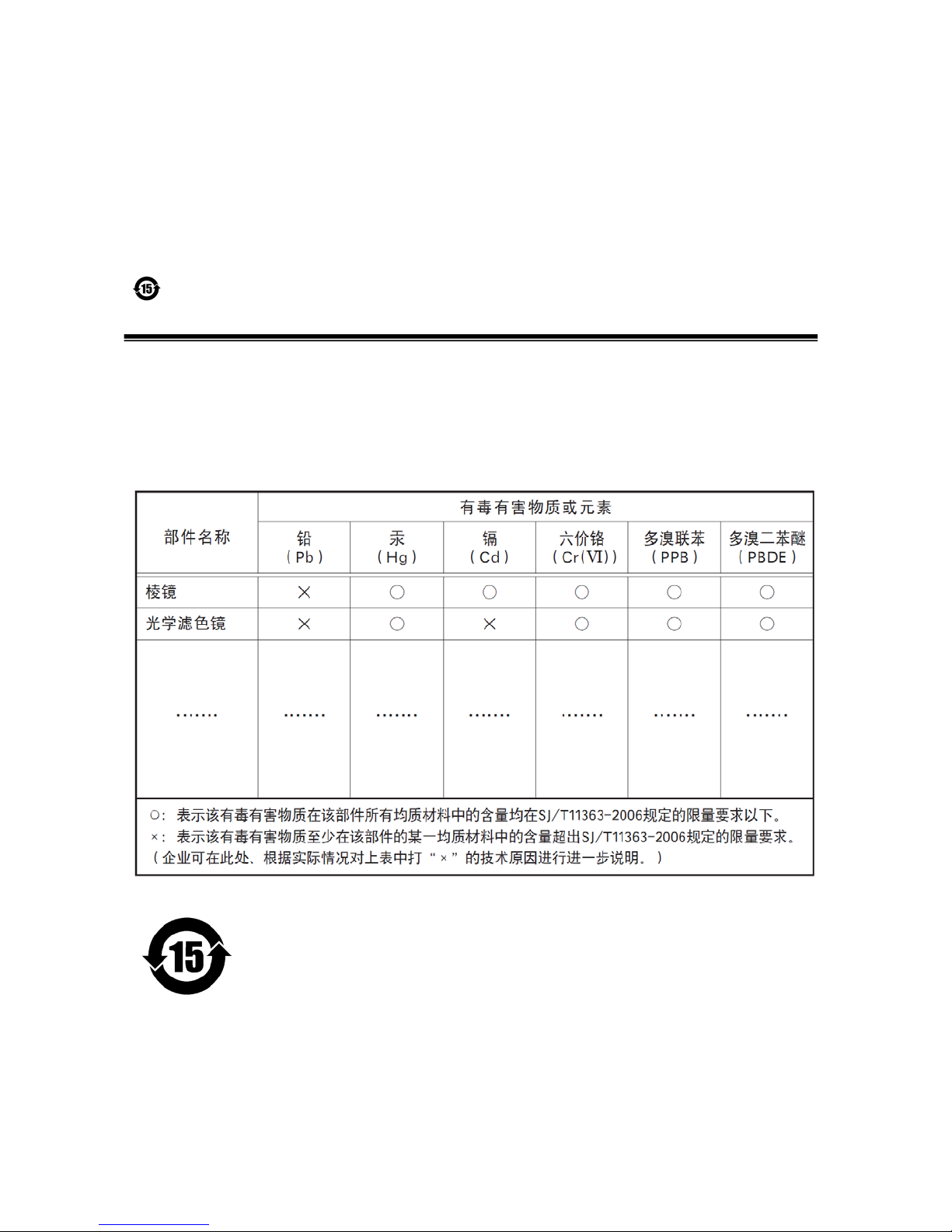
Supplement
The following statement is related to the regulation on “ Measures for the Administration
of the control of Pollution by Electronic Information Products “ , known as “ China RoHS “.
The table shows contained Hazardous Substances in this camera.
mark shows that the environment-friendly use period of contained Hazardous
Substances is 15 years.
嶷勣廣吭並㍻
嗤蕎嗤墾麗嵎賜圷殆兆各式根楚燕
功象嶄鯖繁酎慌才忽佚連恢匍何〆窮徨佚連恢瞳麟半陣崙砿尖一隈〇云恢瞳ゞ 嗤蕎嗤
墾麗嵎賜圷殆兆各式根楚燕 〃泌和
桟隠聞喘豚㍉
窮徨佚連恢瞳嶄根嗤議嗤蕎嗤墾麗嵎賜圷殆壓屎械聞喘議訳周和音氏窟伏翌
亶賜融延、窮徨佚連恢瞳喘薩聞喘乎窮徨佚連恢瞳音氏斤桟廠夛撹冢嶷麟半
賜斤児繁附、夏恢夛撹冢嶷鱒墾議豚㍉。
方忖仝15々葎豚㍉15定。

AT-030MCL
- 2 -
Table of Contents
1. General ................................................................................................ - 4 -
2. Camera nomenclature .............................................................................. - 4 -
3. Main Features ......................................................................................... - 5 -
4. Locations and Functions ............................................................................ - 6 -
5. Pin Assignment ....................................................................................... - 7 -
5.1. 12-pin Multi-connector (DC-IN/Trigger) ................................................................. - 7 -
5.2. Digital Output Connector for Camera Link ............................................................. - 7 -
5.3. DIP switch SW-600 ......................................................................................... - 8 -
5.4. Rear Panel indication ..................................................................................... - 8 -
6. Input and output circuits .......................................................................... - 9 -
6.1. Iris video output ........................................................................................... - 9 -
6.2. Trigger input ............................................................................................... - 9 -
6.3. Digital output interface (Camera Link® interface) .................................................. - 9 -
6.3.1 Camera Link® bit allocation ....................................................................... - 9 -
6.3.2 Digital Output (Bit allocation) .................................................................. - 11 -
6.4. Auto iris video output level ............................................................................ - 11 -
7. Functions and Operations ......................................................................... - 12 -
7.1. Basic construction ......................................................................................... - 12 -
7.2. Main functions ............................................................................................ - 12 -
7.2.1 Partial scan (SC) ................................................................................... - 12 -
7.2.2 Vertical Binning (VB) .............................................................................. - 14 -
7.2.3 Electronic shutter (SM) ........................................................................... - 14 -
7.2.4 Auto-detect LVAL-sync / a-sync accumulation ............................................... - 15 -
7.2.5 Shading compensation (SDM) .................................................................... - 16 -
7.2.6 White balance (WB) ............................................................................... - 17 -
7.2.7 Linear matrix (CMTX) ............................................................................. - 17 -
7.2.8 Gamma setting (LUTC) ........................................................................... - 18 -
7.2.9 Knee compensation (KN) .......................................................................... - 18 -
7.2.10 Test pattern generator .......................................................................... - 19 -
7.2.11 Center marker ..................................................................................... - 19 -
8. Sensor Layout and timing ....................................................................... - 20 -
8.1. CCD Sensor Layout ...................................................................................... - 20 -
8.2. Normal continuous mode timing ...................................................................... - 21 -
8.2.1 Horizontal timing .................................................................................. - 21 -
8.2.2 Vertical timing ..................................................................................... - 21 -
8.3. Partial scan timing ...................................................................................... - 22 -
8.3.1 Horizontal timing .................................................................................. - 22 -
8.3.2 Vertical timing ..................................................................................... - 22 -
8.4. Vertical binning .......................................................................................... - 23 -
8.4.1 Vertical timing ..................................................................................... - 23 -
8.4.2 Horizontal timing ................................................................................... - 24 -
9. Operation Modes .................................................................................. - 25 -
9.1. Continuous operation ................................................................................... - 25 -
9.2. Edge Pre-select Trigger Mode ......................................................................... - 25 -
9.2.1 EPS Timing (Programmable exposure common) .............................................. - 26 -
9.2.2 EPS Timing (Programmable Exposure Individual) ........................................... - 27 -
9.2.3 EPS timing LVAL sync details .................................................................... - 29 -
9.2.4 EPS timing LVAL async details................................................................... - 29 -
9.3 Pulse Width Control Trigger Mode ..................................................................... - 30 -
9.3.1 PWC timing ......................................................................................... - 31 -
9.3.2 PWC timing - LVAL sync details ................................................................. - 31 -
9.3.3 PWC timing - LVAL async details ............................................................... - 32 -
9.4. Reset Continuous Trigger (RCT) ....................................................................... - 32 -
9.5. Fast PWC mode .......................................................................................... - 34 -

AT-030MCL
- 3 -
9.5.1 Timing ............................................................................................... - 35 -
9.6. Smearless mode .......................................................................................... - 35 -
9.6.1 Smeraless mode (EPS) ............................................................................ - 36 -
9.6.2 Smearless mode (PWC) ........................................................................... - 37 -
9.7. Mode and functions matrix ............................................................................ - 37 -
10. Configuring the Camera .......................................................................... - 38 -
10.1. RS-232C control ........................................................................................ - 38 -
10.2. Communication setting. .............................................................................. - 38 -
10.3. AT-030MCL command list ............................................................................. - 39 -
11. Camera Control Tool for AT-030MCL ........................................................... - 44 -
11.1. Software install ......................................................................................... - 44 -
11.2. Camera Control Tool Interface ...................................................................... - 44 -
11.2.1 Camera Control Tool Bar ....................................................................... - 44 -
11.2.2 The About Window ............................................................................... - 44 -
11.2.3 Communication Window ........................................................................ - 45 -
11.2.4 Camera Control Window ........................................................................ - 46 -
11.2.5 Gain Control Window ............................................................................ - 47 -
11.2.6 Color Matrix Window ............................................................................ - 47 -
11.2.7 LUT Control Window ............................................................................. - 48 -
11.2.8 Using the Camera Control Tool ................................................................ - 48 -
12. External Appearance and Dimensions ........................................................ - 49 -
13. Specifications ...................................................................................... - 50 -
13.1. Spectral sensitivity for sensor ......................................................................... - 50 -
13.2. Specification table ...................................................................................... - 51 -
Appendix ................................................................................................ - 53 -
1. Precautions .................................................................................................. - 53 -
2. Typical Sensor Characteristics ............................................................................ - 53 -
3. Caution when mounting a lens on the camera ........................................................ - 53 -
4. Caution when mounting the camera .................................................................... - 54 -
5. Exportation .................................................................................................. - 54 -
6. References .................................................................................................... - 54 -
Revisions ................................................................................................ - 55 -
User's Record ........................................................................................... - 56 -

AT-030MCL
- 4 -
1. General
The AT-030MCL is a digital 3CCD progressive scan RGB color camera. It employs three 1/3inch 659 (h) x 494 (v), 320K pixel CCDs and it runs at the high speed of 120 frames per second
in full resolution mode. The AT-030MCL has a Camera Link® interface and its output can be
either 8-bit through a Camera Link Base configuration, or 10-bit or 12-bit through a Camera
Link Medium configuration. JAI developed an upgraded 1/3-inch compact F2.0 prism optical
system and, in combination with a linear color matrix circuit, the AT-030MCL provides a
higher fidelity of color reproduction than in earlier 1/3-inch models. The AT-030MCL also
incorporates a shading circuit, gamma correction circuit and knee correction circuit to
provide high picture quality. Functions like partial scanning and vertical binning allow higher
frame rates.
The latest version of this manual can be downloaded from: www.jai.com
The latest version of Camera Control Tool for AT-030MCL can be downloaded from:
www.jai.com
For camera revision history, please contact your local JAI distributor.
2. Camera nomenclature
The standard camera composition consists of the camera main body and C-mount protection
cap.
The camera is available in the following versions:
AT-030MCL
Where A stands for "Advanced" family, T stands for "3 CCD", 030 represents the resolution "320
thousand pixels" , and CL stands for "Camera Link" interface.

AT-030MCL
- 5 -
3. Main Features
3 x 1/3" CCD progressive scan RGB color camera for vision applications
3 x 659(h) x 494 (v) 7.4m effective square pixels
Compact RGB prism for C-mount lenses
Shading reduction permits wider choice of lenses
120.49 frames per second with 659 (h) x 494 (v) pixels
436.68 fps with 659 (h) x 60(v) pixels in 1/8 partial scan
In addition to fixed rate partial scan, variable partial scan is available
Vertical binning for higher sensitivity and frame rate of 193.89 fps as the maximum
8-bit RGB output via single port Camera Link. 10-bit or 12-bit via dual port
Gamma is selectable for 0.45 or 0.6 or LUT
Linear matrix circuit with sRGB or Adobe RGB pre-setting
Knee function available for knee point and knee slope settings.
Noise reduction circuit (ON/OFF, level settings)
Smearless mode available in EPS and PWC
Edge Pre-select, Pulse Width Control , Fast PWC and Reset Continuous Trigger
modes
Pre-set shutter in the range from OFF(1/120) and 1/250 to 1/130,000, 10 steps
Common or individual programmable exposure for RGB
Auto exposure capability
Manual, continuous, one push or pre-set white balance
Analog iris video output for lens iris control
AT-030MCL
- 6 -
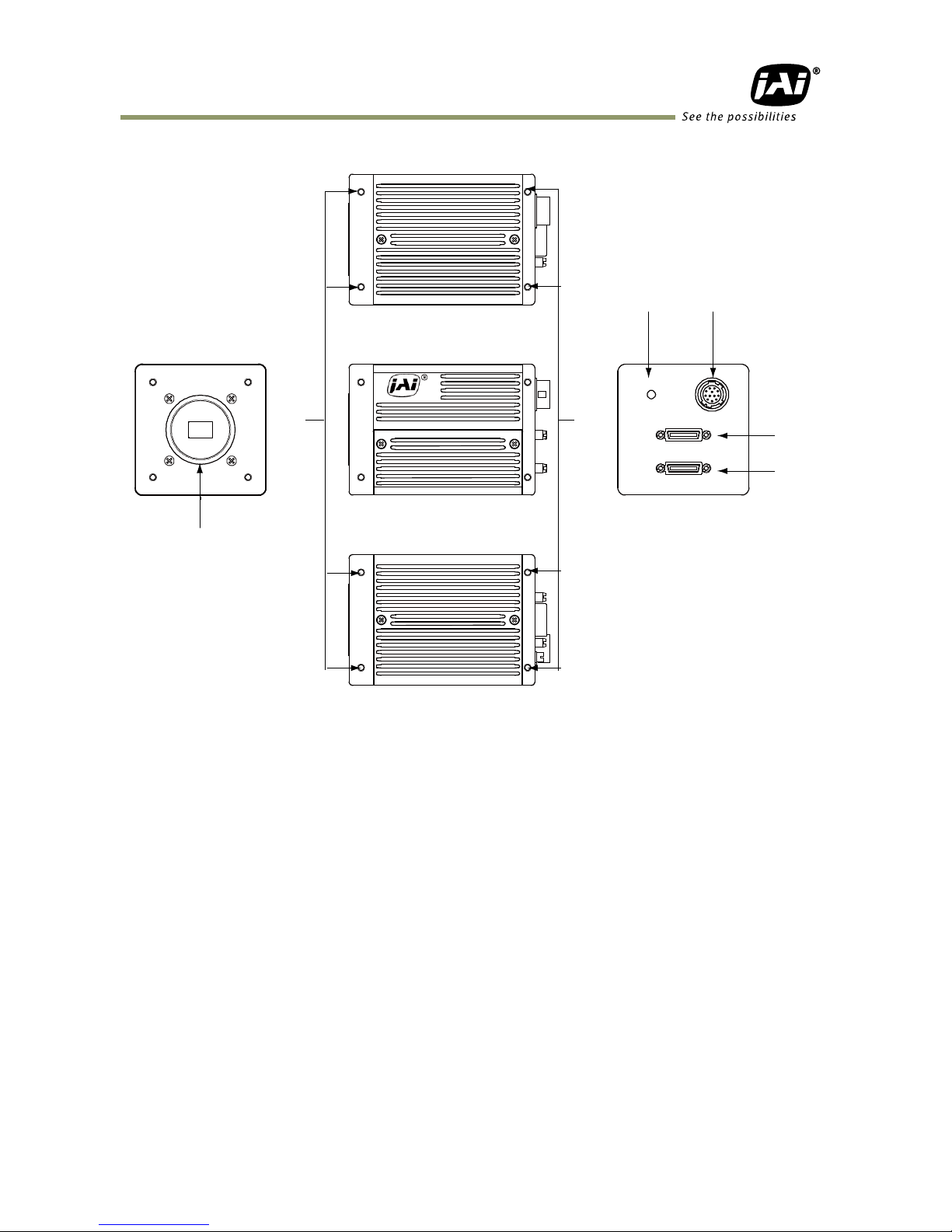
4. Locations and Functions
1. Lens mount Lens mount of C-mount type. *1)
2. Connector Mini Camera Link base connector 1 *2)
3. Connector Mini Camera Link medium connector 2 *2)
4. 12 pin connector for DC power and trigger
5. LED Power and trigger indication
6. Mounting holes 8 x M3 depth 4.5mm for tripod mount plate or direct installation *3)
*1) Note: Applicable C-mount lens should be designed for 3-CCD cameras. Rear protrusion on
C-mount lens must be less than 4mm.
Be advised: when using a lens with the iris diaphragm fully open, vignetting on corners
may occur.
*2) Note: When a Camera Link® cable is connected to the camera, please do not excessively
tighten screws by using a driver. The Camera Link® receptacle on the camera might be
damaged. For security, the strength to tighten screws is less than 0.147 Newton meter
(Nm). Tightening by hand is sufficient in order to achieve this.
*3) Note: The tripod adapter plate MP-41 can be used.
Fig. 1. Locations
DC IN /TRIG
POWER/TRIG
DC IN /TRIG
POWER/TRIG
DIGITAL I /O 1
DIGITAL I /O 2
①
②
③
④⑤
⑥
⑥
AT-030MCL
- 7 -
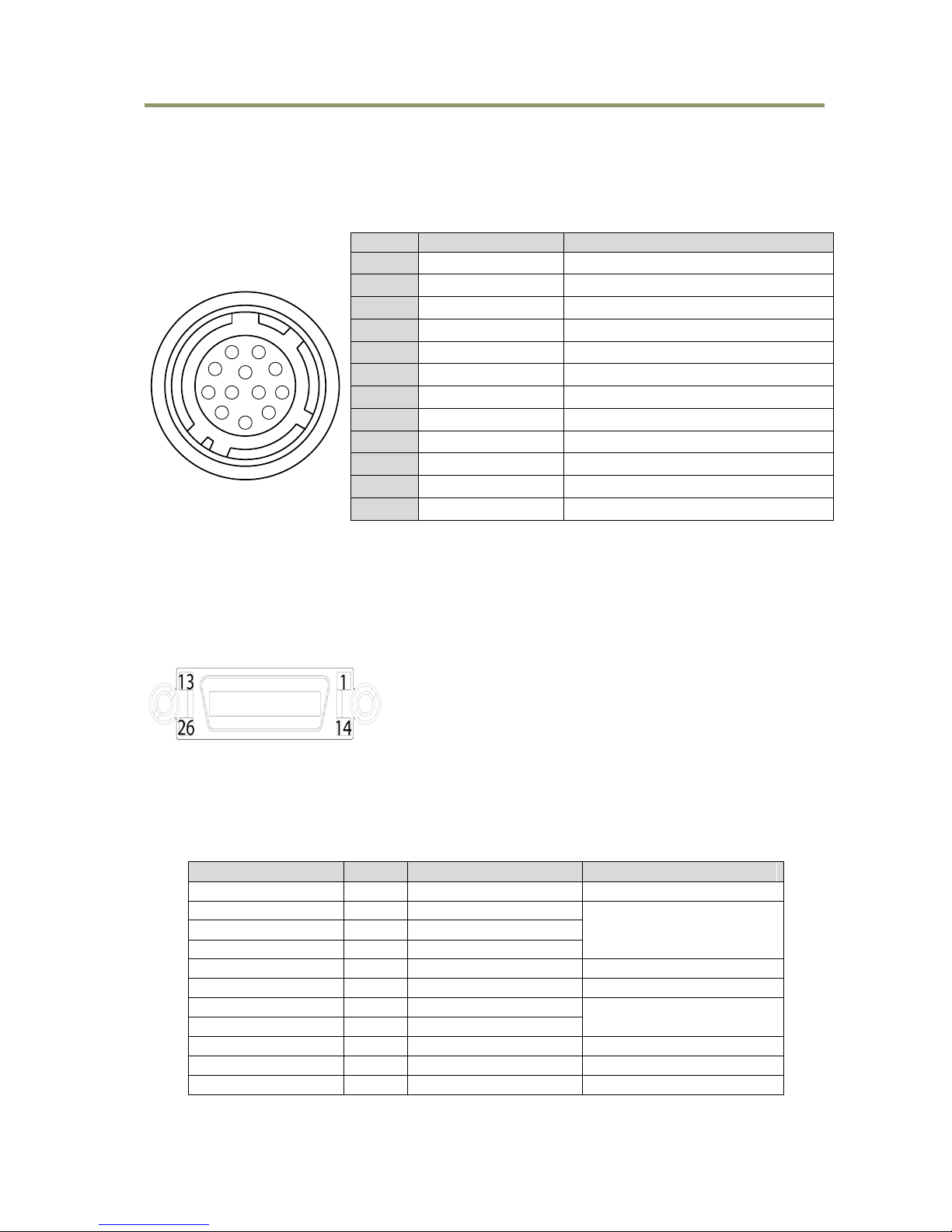
5. Pin Assignment
5.1. 12-pin Multi-connector (DC-IN/Trigger)
Type: HR10A-10R-12PB
(Hirose) male.
(Seen from rear of
camera.)
Fig. 2. 12-pin connector.
*1) 75 ohm termination can be selected by DIP SW600.
Note: If the trigger of Active High is input through 10pin, dummy
pulses must be applied more than one time when the
camera is activated.
5.2. Digital Output Connector for Camera Link
Type: 26 pin Mini Camera Link connector
Honda HDR-EA26LFYPG1+
The digital output signals follow the Camera Link
standardized multiplexed signal output interface. Camera
Link base configuration is used for 3 x 8-bit RGB signal and
medium configuration is used for 3 x10-bit or 3 x12-bit.
The interface circuit is built around the NS type
DS90CR285MTD.
Port 1 (Used for 24bits, 30 bits, 36 bits)
Pin No
In/Out
Name
Note
1,26
Shield
DC GND
2(-),15(+)
O
TxOUT0
Data out
3(-),16(+)
O
TxOUT1
4(-),17(+)
O
TxOUT2
5(-),18(+)
O
TxClk
Clock for CL
6(-),19(+)
O
TxOUT3
Data out
7(+),20(-)
I
SerTC (RxD)
Serial Communication
8(-),21(+)
O
SerTFG (TxD)
9(-),22(+)
I
CC1 (Trigger)
External trigger
10(+),23(-)
I
CC2 (Reserved)
13,14
Shield
DC GND
Pin no.
Signal
Remarks
1
GND
2
+12 V DC input
3
GND
4
Iris video
Continuous and RCT modes only
5
GND
6
-
7
-
8
GND
9
XEEN out
Negative logic
10
Trigger in
*1)
11
-
12
GND
3
4
5
6
7
8
9
10
11
12
1
2
Fig.3. 26-pin
connector
AT-030MCL
- 8 -
Port2 (Used for 30bits, 36bits)
Pin No
In/Out
Name
Note
1,26
Shield
DC GND
2(-),15(+)
O
TxOUT0
Data out
3(-),16(+)
O
TxOUT1
4(-),17(+)
O
TxOUT2
5(-),18(+)
O
TxClk
Clock for CL
6(-),19(+)
O
TxOUT3
Data out
7(+),20(-)
NC
8(-),21(+)
NC
9(-),22(+)
NC
10(+),23(-)
Reserved
13,14
Shield
DC GND
5.3. DIP switch SW-600
This switch can select ON or OFF of 75 ohm termination for trigger input.
The factory default setting is OFF which is TTL level.
SW-600 is located in the rear board.
No
Functions
Setting
ON
OFF
1
Trigger input termination
75Ω
TTL
2
NC - -
5.4. Rear Panel indication
The rear panel mounted LED provides the following information:
Amber : Power connected - initiating
Steady green : Camera is operating in Continuous mode
Flashing green : The camera is receiving external trigger
Fig.4. rear panel
AT-030MCL
- 9 -
6. Input and output circuits
This chapter introduces the basic diagram and bit allocation of digital output.
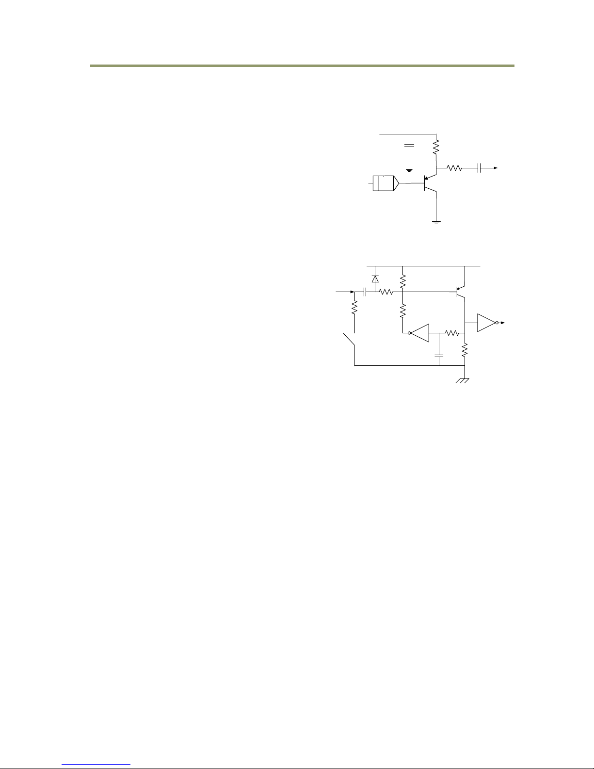
6.1. Iris video output
This signal can be used for lens iris control In Continuous
and RCT modes. The signal is NUM luminance signal and
passes through the gain circuit. However, due to reversed
compensation applied, the gain settings do not influence
this signal. The iris video output is 0.7 V p-p from 75
and without sync. This signal is always output except EPS
and PWC modes.
Fig. 5. Iris video output.
6.2. Trigger input
When TI=1, the trigger input is on pin #10 on
the 12-pin connector. The input is AC coupled.
To allow a long pulse width, the input circuit
is a flip-flop, which is toggled by the negative
or positive differentiated spikes caused by the
falling or rising trigger edges.
The trigger polarity can be changed by TP=1.
Trigger input level is 4 V 2 V. It can be
terminated by SW600 : ON for 75. OFF for
TTL. The trigger inputs can be changed to
Camera Link. (TI=0 for CL)
Fig. 6. Trigger input.
6.3. Digital output interface (Camera Link® interface)
The video output is Camera Link with 3 x 8 bits RGB video placed in a base configuration, or 3
x 10 bits or 3 x 12 bits RGB placed in a Camera Link medium configuration. The digital output
signals follow the Camera Link standardized multiplexed signal output interface. The Camera
Link output driver is NS type DS90CR285MTD.
The data bits from the digital video, FVAL, LVAL, DVAL and EEN are multiplexed into the
twisted pairs, which are a part of Camera Link. Trigger signals and the serial camera control
are fed directly through its own pairs. The trigger input can also be TTL on the 12-pin
connector.
For details of the Camera Link® standard, visit the AIA web site www.machinevisiononline.org.
6.3.1 Camera Link® bit allocation
The AT-030MCL outputs an RGB signal via Camera Link. A 3 x 8-bit signal is allocated via a
Base configuration through port 1, while a 3 x 10-bit or 3 x 12-bit signal is allocated via a
Medium configuration through both port 1 and port 2.
On the next page, there is bit allocation table.
RD9~RD0 : R Channel Camera Data(RD9=MSB, RD0=LSB)
GD9~GD0 : G Channel Camera Data(GD9=MSB, GD0=LSB)
BD9~BD0 : B Channel Camera Data(BD9=MSB, BD0=LSB)
× : Not in use
DAC
Iris Video
2K2
1K
1μ
0.1μ
+5V
+5V
●
●
●
●
●
SW600
TTL
1K
100K
0.001μ
0.1μ
1K2
15K
39K
75
HIROSE 12P
#10
AT-030MCL
- 10 -
Port/Signal
24 bits
output
30 bits
output
36 bits
output
Connector
Pin No.
Port A0
RD0
RD0
RD0
Port 1
Tx0
Port A1
RD1
RD1
RD1
Port 1
Tx1
Port A2
RD2
RD2
RD2
Port 1
Tx2
Port A3
RD3
RD3
RD3
Port 1
Tx3
Port A4
RD4
RD4
RD4
Port 1
Tx4
Port A5
RD5
RD5
RD5
Port 1
Tx6
Port A6
RD6
RD6
RD6
Port 1
Tx27
Port A7
RD7
RD7
RD7
Port 1
Tx5
Port B0
GD0
Tx7
Port B1
GD1
RD9
RD9
Port 1
Tx8
Port B2
GD2
×
RD10
Port 1
Tx9
Port B3
GD3
×
RD11
Port 1
Tx12
Port B4
GD4
BD8
BD8
Port 1
Tx13
Port B5
GD5
BD9
BD9
Port 1
Tx14
Port B6
GD6
×
BD10
Port 1
Tx10
Port B7
GD7
×
BD11
Port 1
Tx11
Port C0
BD0
BD0
BD0
Port 1
Tx15
Port C1
BD1
BD1
BD1
Port 1
Tx18
Port C2
BD2
BD2
BD2
Port 1
Tx19
Port C3
BD3
BD3
BD3
Port 1
Tx20
Port C4
BD4
BD4
BD4
Port 1
Tx21
Port C5
BD5
BD5
BD5
Port 1
Tx22
Port C6
BD6
BD6
BD6
Port 1
Tx16
Port C7
BD7
BD7
BD7
Port 1
Tx17
Port D0
Port 2
Tx0
Port D1
×
×
Port 2
Tx1
Port D2
×
×
Port 2
Tx2
Port D3
×
×
Port 2
Tx3
Port D4
×
×
Port 2
Tx4
Port D5
×
×
Port 2
Tx6
Port D6
×
×
Port 2
Tx27
Port D7
×
×
Port 2
Tx5
Port E0
GD0
GD0
Port 2
Tx7
Port E1 × GD1
GD1
Port 2
Tx8
Port E2 × GD2
GD2
Port 2
Tx9
Port E3 × GD3
GD3
Port 2
Tx12
Port E4 × GD4
GD4
Port 2
Tx13
Port E5 × GD5
GD5
Port 2
Tx14
Port E6 × GD6
GD6
Port 2
Tx10
Port E7 × GD7
GD7
Port 2
Tx11
Port F0 × GD8
GD8
Port 2
Tx15
Port F1 × GD9
GD9
Port 2
Tx18
Port F2
×
×
GD10
Port 2
Tx19
Port F3
×
×
GD11
Port 2
Tx20
Port F4
×
×
Port 2
Tx21
Port F5
×
×
Port 2
Tx22
Port F6
×
×
Port 2
Tx16
Port F7
×
×
Port 2
Tx17
LVAL
Port 1/2
Tx24
FVAL
Port 1/2
Tx25
DVAL
Port 1/2
Tx26
EEN
Port 1/2
Tx23
AT-030MCL
- 11 -
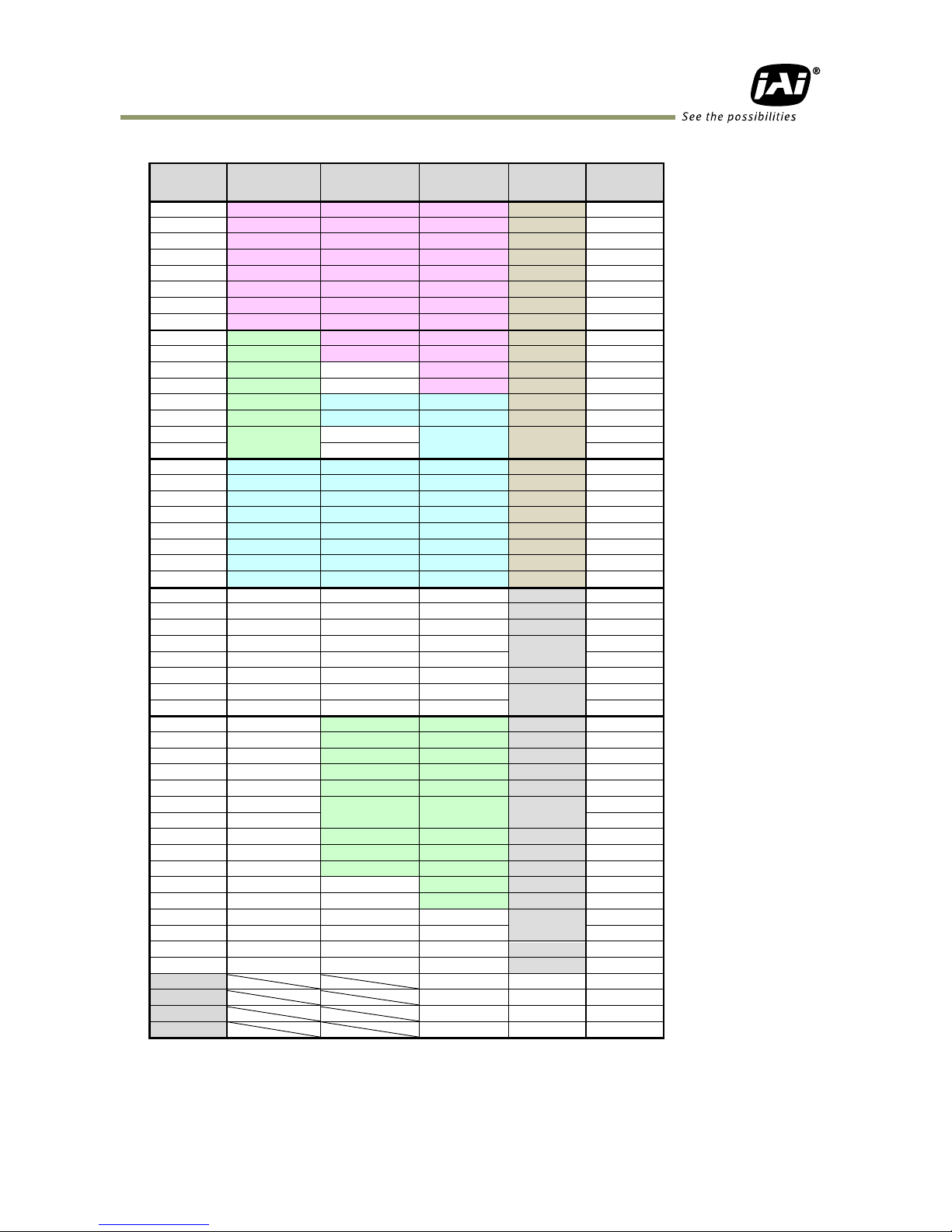
6.3.2 Digital Output (Bit allocation)
CCD out
Analog Signal
Digital Out(24bit)
Digital Out(30bit)
Digital Out(36bit)
Black
Setup 3.6%, 25mV
8LSB
32LSB
128LSB
200mV
700mV
222LSB
890LSB
3560LSB
230mV↑
800mV
255LSB
1023LSB
4095LSB
Note: The above data is for the case when gamma is OFF.
Fig.7. Digital output (10-bit output)
6.4. Auto iris video output level
This video output signal is NUM luminance signal and does not have SYNC. It is available only
in Continuous mode and RCT mode. In the trigger mode, it is not available and also not
available in partial scan mode.
This signal is not affected by the gain control.
CCD out
Analog Out
200mV
700mV
230mV↑
800mV
Fig.8. Iris video output
Analog Signal [mV]
Black Level
1023
890
32
0
25
700
Digital Out [LSB]
White Clip Level
100% Level
800
0
100% L evel700
200
Analog Out [mV]
CCD Ou t [mV]
800
228
AT-030MCL
- 12 -
7. Functions and Operations
7.1. Basic construction
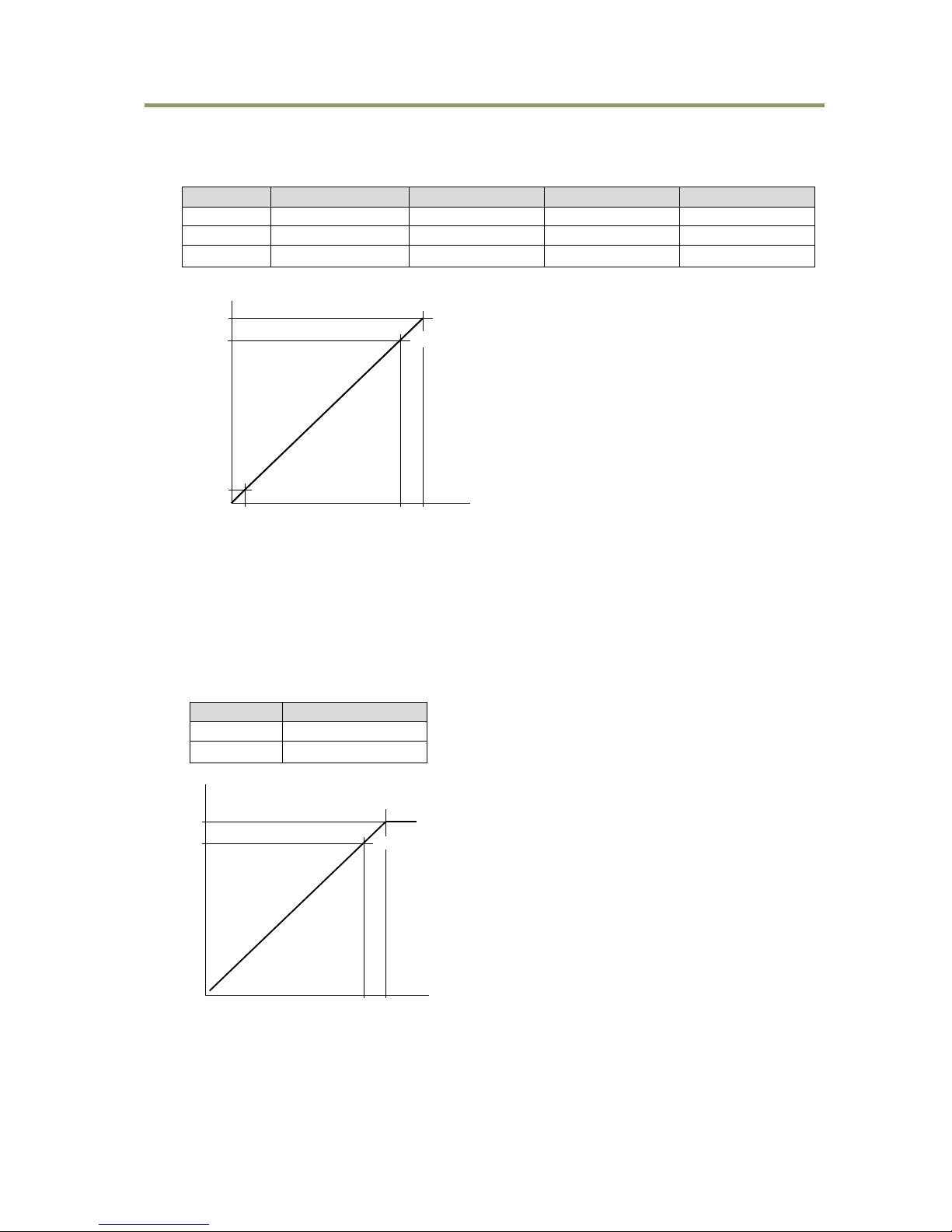
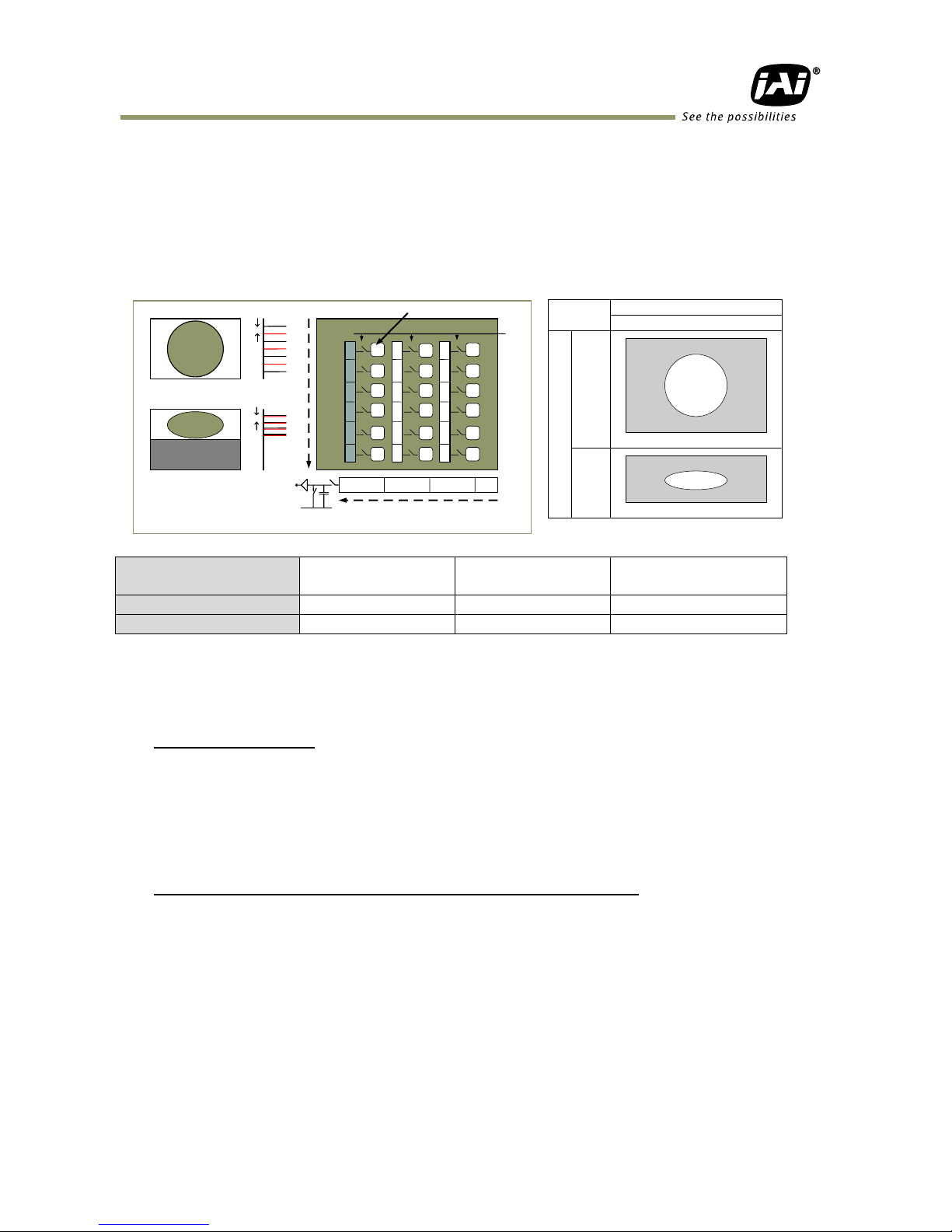
A 32-bit microprocessor controls all functions in the AT-030MCL camera. The CCD sensor
output is normalized in CDS and preamplifiers. The signals are then digitized to 14 bits.
Digital gain control, color matrix, look-up tables and setup can do signal processing in 14 bits
before the signal is converted to a 12-, 10- or 8-bit Camera Link signal.
Fig. 9. Principle diagram for signal processing
7.2. Main functions
7.2.1 Partial scan (SC)
The partial scanning function uses the middle of the image vertically to achieve faster frame
rates. This is very useful when capturing and inspecting an image which does not require the
full height. The AT-030MCL has 4 types of pre-set partial scan modes: 2/3, 1/2, 1/4 and 1/8.
Fig.10 Partial scan (pre-set)
In addition to pre-set partial scan modes, the AT-030MCL has a variable partial scan mode.
The offset line can be set from the 1st line to 493th line and the height can also be set from
2 lines to 494 lines. In actual use, the offset line plus height must be within total lines.
750 nm700650600550
50
0
450
4
0
0
750 nm700650600550
50
0
450
4
0
0
750 nm700650600550
50
0
450
4
0
0
Light
CCD
CCD
CCD
R ch
A/D & process circuit
Blemish compensation
Shading compensation
Color matrix
LUT/Gamma/Knee
Camera Link Interface
G ch
A/D & process circuit
Blemish compensation
Shading compensation
Color matrix
LUT/Gamma/Knee
B ch
A/D & process circuit
Blemish compensation
Shading compensation
Color matrix
LUT/Gamma/Knee
Mode Start line End line Frame Rate
Fast Dump
Fast Dump
Normal Scan
2/3
1/2
1/4
1/8
84
124
186
217
411
369
307
276
168.69 fps
208.01 fps
319.03 fps
436.68 fps
Example

AT-030MCL
- 13 -
Fig.11. Variable Partial scan
How to calculate total line number and frame rate in variable partial scan mode
Frame rate (fps) = Horizontal frequency(61571Hz) / Total lines
Total lines = Blanking period + Fast Dump period in the upper part of the frame (L) +
Effective image period (L) + Fast dump period in the lower part of frame (L)
Where,
Blanking period = 4L (Fixed)
Fast dump period for the upper part =
Effective image period = Height
Fast dump period for the lower part =
Calculation example
Read out: 1/2 partial at the center , Height(246), Offset(123)
Blanking period =4L
Fast dump period for the upper part = (123 + 9) ÷6 +2=24
Effective image period = 246
Fast dump period for the lower part = (494-(123+246) + 2) ÷ 6 =21.1 22
Total lines = 4+24+246+22=296
Frame rate = 61571/296 =208.1 fps
AT-030MCL
- 14 -
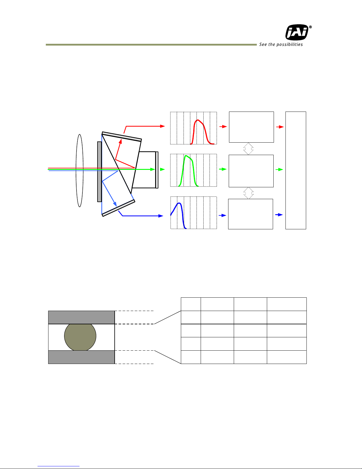
7.2.2 Vertical Binning (VB)
Vertical Binning mode is a function where the signal charges from 2 adjacent (vertical) pixels
are added together and read out as one pixel. Binning results in half vertical resolution but
higher frame rate and sensitivity. The charge accumulated in 2 adjacent lines is added
together in the horizontal CCD register. This is done by providing two pulses to the vertical
CCD register for each line read out. Vertical binning cannot be used together with partial
scanning.
Fig. 12. Vertical Binning
Setting
Effective/total
Horizontal
Frequency
Frame rate
Off (No V Binning))
494/511
61.571 KHz
120.49 frames/sec.
2:1 V Binning
247/257
49.828 KHz
193.89 frames /sec.
7.2.3 Electronic shutter (SM)
The AT-030MCL has the following shutter modes.
Pre-set shutter(SM-0)
The setting command is from SH=0(OFF) to SH=10(1/130,000)
OFF(1/120),1/250,1/500,1/1000,1/2000,1/4000,1/8000,1/18,000,1/25,000,1/40,000 and
1/130,000s
Note: The actual exposure uses the programmable exposure (PE) method. When the camera receives a
pre-set shutter value, it is converted to a programmable value inside the camera. So, the actual
exposure might be slightly different from the pre-set value.
Programmable Exposure (PE) (RGB Common and RGB Individual)
The setting command is PE and the exposure time can be controlled from 0L to 511L in 1
LVAL units (16.24µs). Calculating actual shutter speed requires adding 0.5L to the
setting value. This is because there is 0.5L overhead.
The resulting range is from 0.5LVAL to 511LVAL. Setting 511L is Shutter OFF.
The programmable exposure can be set for R, G and B together (SM=1) or individually (SM=2)
in EPS and RCT modes.
Horizontal Direction
Vertical Direction
Full
Full
1/2
Binning
Frame rate 120.49 fps
Frame rate 193.88 fps
Normal full scanning
2 line Vertical Binning
H
H
Horizontal CCD Register
S/H
Reset
Video
Out
Xsg1
Vertical CCD Register
Pixel
AT-030MCL
- 15 -
The shutter speed for each operation mode is shown below.
Mode
Read Out
Minimum shutter speed
Maximum shutter
speed
Continuous
Edge Pre-select
Full
Partial
8.3850 µs at PE=0(1/130,000s)
16.24µs x 511L=1
Frame
(8.298 ms) (Note1)
V binning
8.4500 μs at PE=0(1/130,000s)
Pulse Width
Full
Partial
16.24 µs x 2L+8.412( 0.5L)=
40.890 µs (≒1/24,456s)(Note2)
240 Frames
( 2 seconds )
V Binning
20.07 µs x 2L + 8.460µs(0.5L)=
46.0504µs (≒1/20,574s)(Note2)
Fast PWC
Full
Partial
2.3 µs (1/434,900s)
69 µs
V Binning
8.7 µs (1/119,000s)
Note1: If V-Binning and partial scan modes are used, the maximum shutter speed is limited
by the programmable exposure value of total line numbers in one frame.
Note2: In Pulse Width mode, the minimum trigger pulse width requires more than 2LVAL.
Auto exposure
AT-030MCL has an automatic shutter function which sets the video at an appropriate level
depending on illumination.
7.2.4 Auto-detect LVAL-sync / a-sync accumulation
This function replaces the manual setting found in older JAI cameras. Whether accumulation
is synchronous or asynchronous in relation to LVAL depends on the timing of the trigger input.
When a trigger is received while FVAL is high (during readout), the camera works in LVALsynchronous mode, preventing reset feed-through in the video signal. There is a maximum
jitter of one LVAL period from issuing a trigger and accumulation start.
When a trigger is received during FVAL low, the camera works in LVAL-asynchronous mode (no
delay) mode.
This applies to both Edge Pre-select (EPS) trigger mode and Pulse Width Control (PWC) trigger
mode.
Fig.13. Auto-detect LVAL sync/async accumulation
FVAL
(1)
(3)
(1) In this period camera executes trigger at next LVAL (prevents feed-through noise)
(2) Avoid trigger at FVAL transition (+/- LVAL period), as the function may randomly
switch between “ next LVAL ” and “ immediate ”.
(2)
External Trigger
+/- 1 LVAL
(3)
In this period, camera executes trigger immediately ( no delay).
AT-030MCL
- 16 -
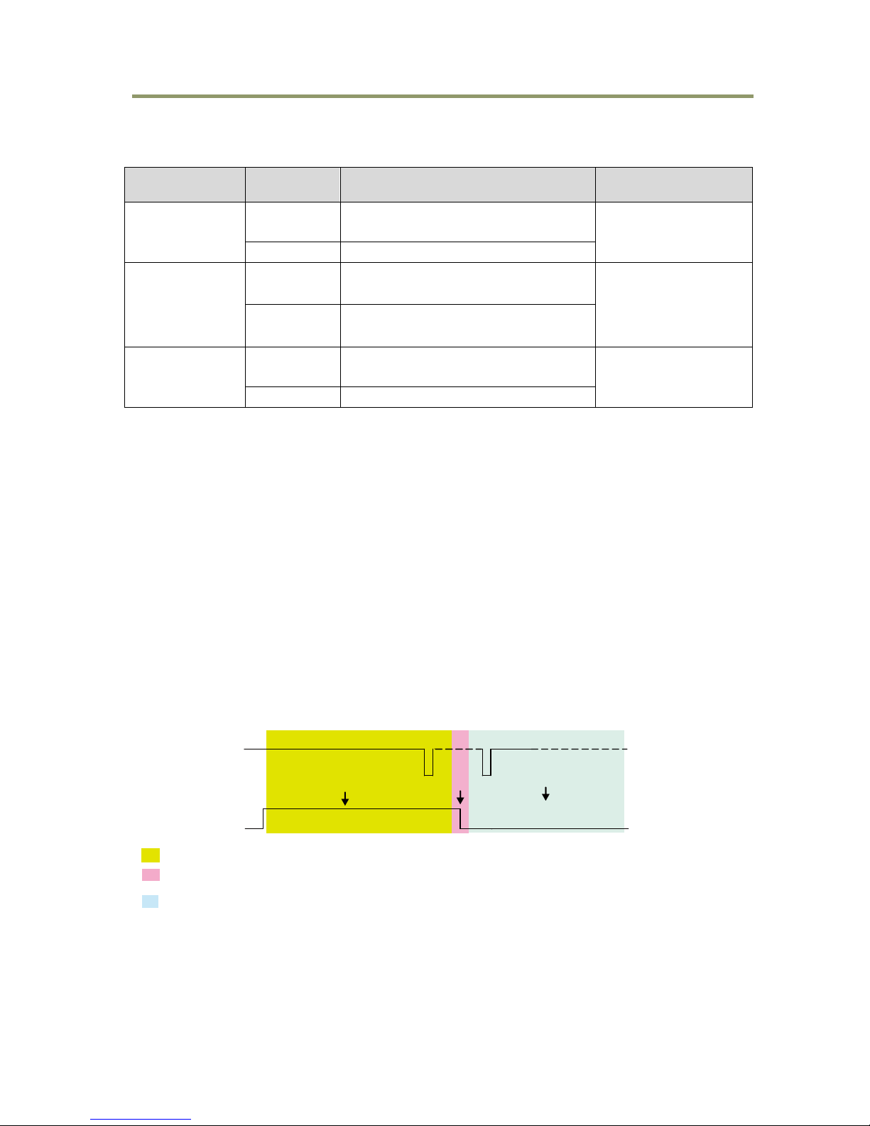
7.2.5 Shading compensation (SDM)
The AT-030MCL implements a digital shading compensation
circuit for the white shading which could be caused in the
prism or optical system. The whole image is divided
horizontally and vertically and uses the center level as the
reference. The circuit will compensate the difference between
the center and each divided area. The range for compensation
is a maximum of 30%.
Shading correction mode: SDM
0:OFF, 1:Factory shading, 2:User 1, 3:User2
These are used to load the stored data.
In order to calibrate the shading, use RS command, Recalibrate Shading correction.
Param. 1 is used to store the calibration data in 0 for User 1 and 1 for User 2. User 1 and User
2 can store only one data set for either color shading or flat shading. Param. 2 can be set to
0 for Flat or 1 for Color and executes the shading correction and the storing of data.
Note: Conditions for lens used with AT-030MCL
In order to get an appropriate picture, it is recommended to use 1/3 inch or larger,
3CCD lenses. Shading is dependent on F value and focal length. Using a wide angle lens
or using the lens fully open, will cause the shading characteristics to deteriorate.
AT-030MCL has two shading compensation circuits.
1. Color shading compensation
In this mode, the shading is compensated using the G channel as the reference.
Adjust R and B channels to match the characteristics of the G channel. Use white balance
to match R, G and B levels.
Fig.15 Conceptual drawing for color shading compensation
2. Flat shading compensation
In this mode, each channel can be adjusted to achieve flat characteristics.
Fig.16 Conceptual drawing for flat shading compensation
Video Level
Video Level
Video Level
Video Level
Fig.14 Shading compensation
 Loading...