IXYS XIGP 2N100 Service Manual

查询IXGP2N100供应商
High Voltage IGBT
IXGP 2N100 1000 V 2.0 A 2.7 V
IXGP 2N100A 1000 V 2.0 A 3.5 V
Symbol Test Conditions Maximum Ratings
V
CES
V
CGR
V
GES
V
GEM
I
C25
I
C90
I
CM
SSOA V
(RBSOA) Clamped inductive load @ 0.8 V
P
C
T
J
T
JM
T
STG
TJ= 25°C to 150°C 1000 V
TJ= 25°C to 150°C; R
= 1 MW 1000 V
GE
Continuous ±20 V
Transient ±30 V
TC= 25°C 4 A
TC= 90°C 2 A
TC= 25°C, 1 ms 8 A
= 15 V, TJ = 125°C, RG = 150W I
GE
= 6 A
CM
CES
TC= 25°C 25 W
-55 ... +150 °C
150 °C
-55 ... +150 °C
Weight 4g
Max. Lead Temperature for 300 °C
Soldering (1.6mm from case for 10s)
Symbol Test Conditions Characteristic Values
(TJ = 25°C unless otherwise specified) Min. Typ. Max.
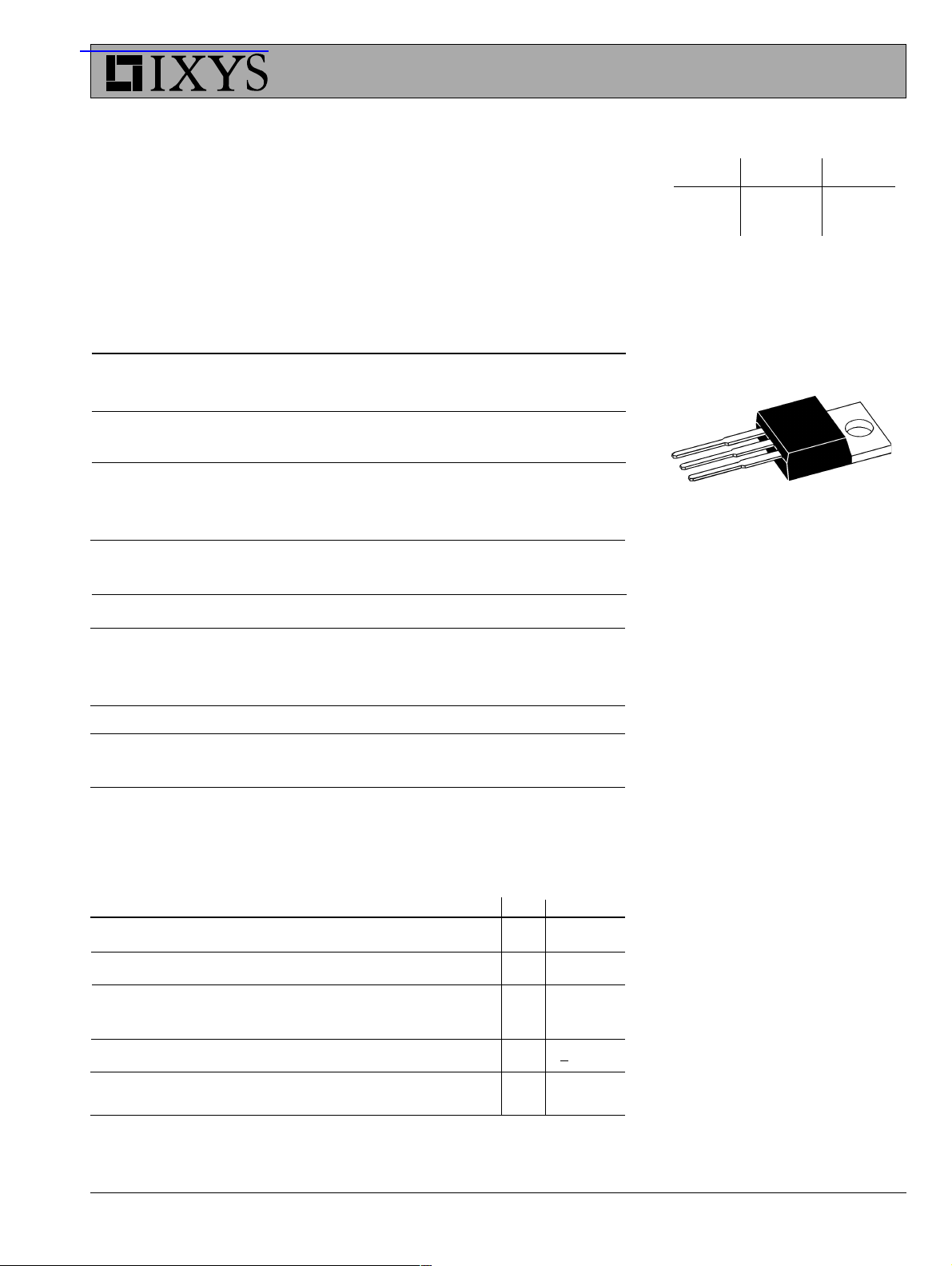
TO-220
1
2
1 = Gate 2 = Collector
3 = Emitter 4 = Collector
Features
International standard package
Low V
- for low on-state conduction losses
High current handling capability
MOS Gate turn-on
- drive simplicity
V
CES
I
C90
V
CE(SAT)
4
3
CE(sat)
BV
V
I
CES
CES
GE(th)
IC= 25µA, V
IC= 25µA, VCE = V
VCE= 0.8 V
CES
VGE= 0 V TJ= 125°C 200 µA
I
GES
V
CE(sat)
© 2000 IXYS All rights reserved
VCE= 0 V, VGE = ±20 V + 50 nA
IC = I
, VGE = 15 V IXGP2N100 2.7 V
C90
= 0 V 1000 V
GE
GE
2.5 5.0 V
TJ= 25°C 10 µA
IXGP2N100A 3.5 V
Applications
Capacitor discharge
Anode triggering of thyristors
DC choppers
Switched-mode and resonant-mode
power supplies.
95514C (9/00)

IXGP 2N100
IXGP 2N100A
Symbol Test Conditions Characteristic Values
= 25°C unless otherwise specified) Min. Typ. Max.
(T
J
g
fs
IC= I
, VCE = 10 V, 0.7 1.5 S
C90
Pulse test, t < 300 µs, duty cycle < 2 %
C
C
C
Q
Q
Q
t
t
t
t
ies
oes
res
g
ge
gc
d(on)
ri
d(off)
fi
VCE= 25 V, VGE = 0 V, f = 1 MHz 101 pF
12 pF
1.8 pF
IC= I
c90
, V
GE
= 15 V, V
= 0.5 V
CE
CES
7.8 nC
1.5 nC
4.2 nC
Inductive load, TJ = 25°C 15 n s
IC= I
, VGE = 1 5 V 20 n s
C90
RG= 150 W 300 600 ns
VCLAMP = 0.8 V
CES
IXGP2N100 560 1000 n s
IXGP2N100A 180 360 ns
E
off
Note 1 IXGP2N100 0.56 1.2 mJ
IXGP2N100A 0.26 0.6 mJ
t
t
E
t
t
d(on)
ri
(on)
d(off)
fi
Inductive load, TJ = 125°C 15 ns
IC= I
RG= R
VCLAMP = 0.8 V
= 15 V 25 n s
C90, VGE
= 150 W 0.3 mJ
(off)
CES
400 n s
Note 1 IXGP2N100 800 n s
IXGP2N100A 360 n s
IXGP2N100 1.0 mJ
E
off
IXGP2N100A 0.5 mJ
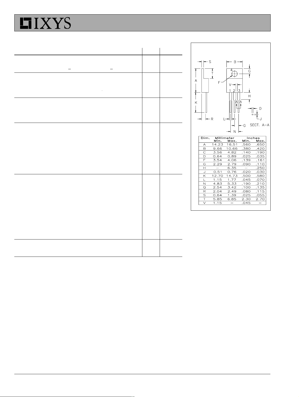
TO-220 Outline
R
thJC
R
thJA
Notes: 1. Switching times may increase for VCE (Clamp) > 0.8 V
higher TJ or increased R
The data herein reflects the advanced objective technical specification and characterization data from engineering lots.
G.
CES
,
5 K/W
110 K/W
IXYS reserves the right to change limits, test conditions, and dimensions.
IXYS MOSFETS and IGBTs are covered by one or more of the following U.S. patents: 4,835,592 4,881,106 5,017,508 5,049,961 5,187,117 5,486,715
4,850,072 4,931,844 5,034,796 5,063,307 5,237,481 5,381,025
 Loading...