

IXYS VTO175-16IO7, VTO175-14IO7, VTO110-14IO7, VTO175-12IO7, VTO110-12IO7 Datasheet

© 2000 IXYS All rights reserved
1 - 2
Data according to IEC 60747 and refer to a single thyristor/diode unless otherwise stated.
IXYS reserves the right to change limits, test conditions and dimensions.
V
RSM
V
RRM
Type
V
DSM
V
DRM
V V
1300 1200 VTO 110-12io7 VTO 175-12io7
1500 1400 VTO 110-14io7 VTO 175-14io7
1700 1600 VTO 175-16io7
Features
●
Package with screw terminals
●
Isolation voltage 3000 V~
●
Planar passivated chips
●
UL registered E72873
Applications
●
Input rectifier for PWM converter
●
Input rectifier for switch mode power
supplies (SMPS)
●
Softstart capacitor charging
Advantages
●
Easy to mount with two screws
●
Space and weight savings
●
Improved temperature and power
cycling
I
dA VM
= 110/167 A
V
RRM
= 1200-1600 V
Symbol Test Conditions Maximum Ratings
VTO 110 VTO 175
I
dAV
TC = 85°C; module 110 167 A
I
FRMS
, I
TRMS
per leg 58 89 A
I
FSM
, I
TSM
TVJ = 45°C; t = 10 ms (50 Hz), sine 1150 1500 A
VR = 0 t = 8.3 ms (60 Hz), sine 1230 1600 A
T
VJ
= T
VJM
t = 10 ms (50 Hz), sine 1000 1350 A
VR = 0 t = 8.3 ms (60 Hz), sine 1070 1450 A
I
2
t TVJ = 45°C t = 10 ms (50 Hz), sine 6600 11200 A2s
VR = 0 t = 8.3 ms (60 Hz), sine 6280 10750 A2s
T
VJ
= T
VJM
t = 10 ms (50 Hz), sine 5000 9100 A2s
VR = 0 t = 8.3 ms (60 Hz), sine 4750 8830 A2s
(di/dt)
cr
TVJ = T
VJM
repetitive, IT = 50 A 150 A/ms
f =400 Hz, tP =200 ms
VD = 2/3 V
DRM
IG = 0.3 A, non repetitive 500 A/ms
diG/dt = 0.3 A/ms, IT = 1/3 • I
dAV
(dv/dt)
cr
TVJ = T
VJM
; VDR = 2/3 V
DRM
1000 V/ms
RGK = ¥; method 1 (linear voltage rise)
V
RGM
10 V
P
GM
TVJ = T
VJM
tp =30ms £ 10 W
IT = I
TAVM
tp = 500 ms £ 5W
tp =10ms £ 1W
P
GAVM
0.5 W
T
VJ
-40...+125 °C
T
VJM
125 °C
T
stg
-40...+125 °C
V
ISOL
50/60 Hz, RMS t = 1 min 2500 V~
I
ISOL
£ 1 mA t = 1 s 3000 V~
M
d
Mounting torque (M6) 5-15 Nm
Terminal connection torque (M6) 5-15 lb.in.
Weight typ. 300 g
VTO 110
VTO 175
Three Phase Full Controlled
Rectifier Bridge, B6C
A
+
B
-
1
2
3
4
5
6
E
~
D
~
C
~
A
B
2
31
5
4
6
E
D
C
© 2000 IXYS All rights reserved
2 - 2
10
-3
10
-2
10
-1
10
0
10
1
0.0
0.1
0.2
0.3
0.4
0.5
0.6
0.7
10
-3
10
-2
10
-1
10
0
10
1
100
200
300
400
500
600
700
800
900
A
s
I
FSM
t
s
t
K/W
Z
thJC
50 Hz
80% V
RRM
TVJ = 45°C
TVJ = 125°C
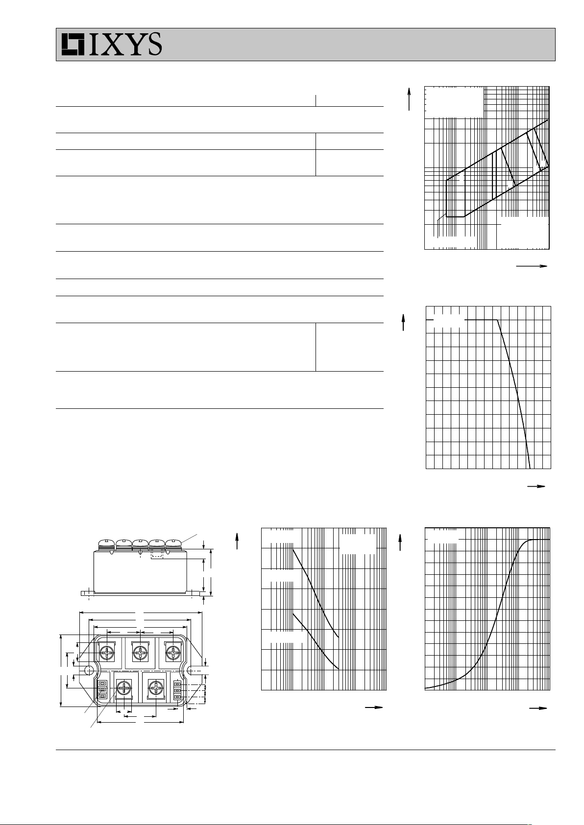
M6x10
7
3
30
27
6.5
6.5
C~
D~ E~
A+
B-
54
15
12
25
66
26
26
72
80
94
4
5
6
3
1
2
5
5
6
7
2.8 x 0.8
M6
Dimensions in mm (1 mm = 0.0394")
Symbol Test Conditions Characteristic Values
VTO 110 VTO 175
IR, I
D
VR = V
RRM
; VD = V
DRM
TVJ = T
VJM
£ 5mA
TVJ = 25°C £ 0.3 mA
V
F
, V
T
IF, IT = 200 A, TVJ = 25°C £ 1.75 1.57 V
V
T0
For power-loss calculations only 0.85 0.85 V
r
T
(TVJ = 125°C) 6 3.5 mW
V
GT
VD = 6 V; TVJ = 25°C £ 1.5 V
TVJ = -40°C £ 1.6 V
I
GT
VD = 6 V; TVJ = 25°C £ 100 mA
TVJ = -40°C £ 200 mA
V
GD
TVJ = T
VJM
;VD = 2/3 V
DRM
£ 0.2 V
I
GD
TVJ = T
VJM
;VD = 2/3 V
DRM
£ 5mA
I
L
IG = 0.3 A; tG = 30 msTVJ = 25°C £ 450 mA
diG/dt = 0.3 A/ms
I
H
TVJ = 25°C; VD = 6 V; RGK = ¥£200 mA
t
gd
TVJ = 25°C; VD = 1/2 V
DRM
£ 2 ms
IG = 0.3 A; diG/dt = 0.3 A/ms
R
thJC
per thyristor (diode); DC current 0.65 0.46 K/W
per module 0.108 0.077 K/W
R
thJH
per thyristor (diode); DC current 0.8 0.55 K/W
per module 0.133 0.092 K/W
d
S
Creeping distance on surface 10 mm
d
A
Creepage distance in air 9.4 mm
a Max. allowable acceleration 50 m/s
2
VTO 110
VTO 175
Fig. 1 Gate trigger characteristics
Fig. 2 DC output current at case
temperature
Fig. 3 Surge overload current
I
FSM
: Crest value, t: duration
Fig. 4 Transient thermal impedance
junction to case (per leg)
VTO 110
VTO 110
1 10 100 1000
0.1
1
10
I
G
V
G
mA
1: I
GT
, T
VJ
= 125°C
2: I
GT
, T
VJ
= 25°C
3: I
GT
, T
VJ
= -40°C
V
4: P
GAV
= 0.5 W
5: P
GM
= 5 W
6: P
GM
= 10 W
I
GD
, T
VJ
= 125°C
4
2
1
5
6
3
0 50 100 15
0
0
20
40
60
80
100
120
A
I
dAV
°C
T
C
VTO 110
 Loading...