IXYS PVX-2505 Datasheet

THE PULSE OF THE FUTURE
DIRECTED
ENERGY
INCORPORATED
• Output Voltage To +50V
• Output Current To 10A
• 50% Maximum Duty Cycle
• Pulse widths from <1 µµS to 100µµS
• Instrument-quality analog voltage
and current monitors for data
acquisition
• Designed for precision pulsing of
semiconductor devices for
pulsed I-V characterization
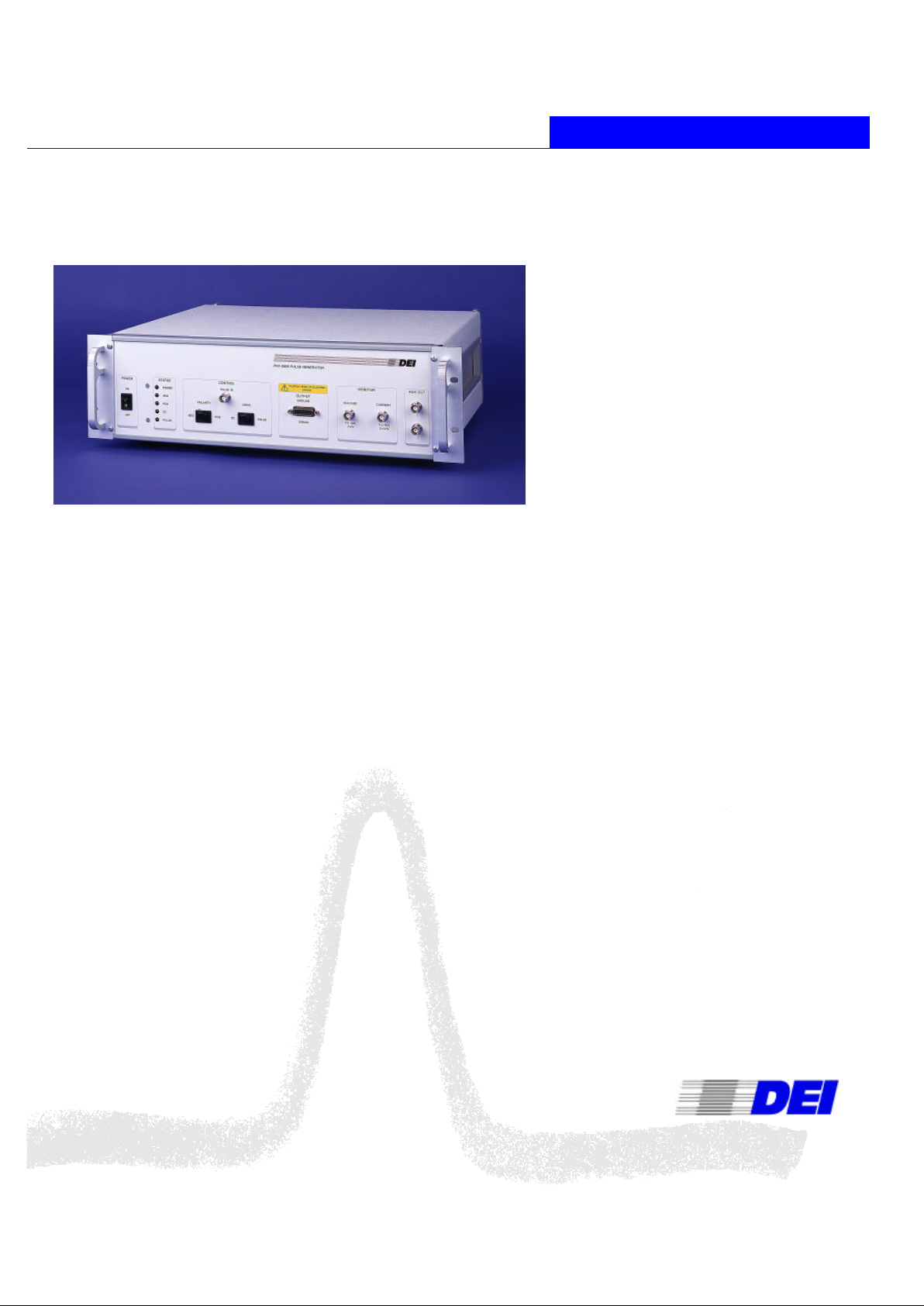
PVX-2505
50V, 10A PRECISION PULSED I-V PULSE GENERATOR
The PVX-2505 pulse generator is designed for pulsed I-V
(current-voltage) characterization of semiconductor
devices at up to 50 Volts and 10 Amps. It is also well
suited for other applications requiring high current,
precision voltage pulses.
The I-V char acteristics of semiconductor devices are
functions of frequency and temperature. Curve tracers
and other "DC" test systems typically step through a
range of gate voltages and, at each gate voltage, sweep
the drain voltage over the measurement range. The
device essentially reaches thermal equilibrium and
electronic (semiconductor-trap) equilibrium at each point,
yielding different test characteristics than actual RF
operational characteristics.
By pulsing the device using the PVX-2505 and taking a
measurement during the pulse, the measurements can be
taken before the device heats up. This circumvents the
thermal effects associated with conventional "DC" testing,
more closely approximates the characteristics of the
device when operating at high frequencies, and doesn't
activate the semiconductor "traps".
The PVX-2505 is designed using a bi-directional
MOSFET output stage using DEI’s DE -Series Fast Power
MOSFETs. This design provides fast rise and fall times,
with minimal overshoot, undershoot and ringing and fast
settling times . This controlled voltage waveform allows
the device under test (DUT) to stabilize at voltage within a
few hundred nanoseconds, allowing I-V measurements to
be made before device heating begins.
A quiescent (bias) voltage may be applied to the pulse
generator, allowing the DUT to be held at a voltage other
than zero, then pulsed above or below this voltage.
The PVX-2505 requires an input gate signal, pulse
(VHIGH) and optional quiescent (VLOW) DC power supply
inputs. The output pulse width and frequency are controlled
by the input gate signal. The output voltage amplitud e is
controlled by the amplitude of the input VHIGH and optional
VLOW DC power supply amplitudes.
The front panel controls and monitors provide the flexibility
to operate in pulsed mode, or to switch to DC mode, in
which the DC voltage generated by the VHIGH power
supply is applied directly to the DUT. Integral instrument quality voltage and current probes are provided to facilitate
pulse data acquisition.
The output pulse is launched on an innovative, lowimpedance cable. The design of this cable maintains the
fidelity of the output pulse without introducing pulse
distortion or ringing, and provides a convenient means of
connecting the pulse generator to the DUT or bias tee.
The pulse generator is a direct-coupled, air-cooled solid state design, offering equally fast pulse rise and fall times,
low power dissipation, and minimal over-shoot, under -shoot
or ringing. It has over-current detection and shut -down
circuitry to protect the pulse generator from potential
damage due to arcs and shorts in the load or interconnect
cable.

THE PULSE OF THE FUTURE
Directed Energy, Inc.
An IXYS Company
2401 Research Blvd., Suite 108
Fort Collins, CO USA 80526
970-493-1901 Fax: 970-493-1903
Email: deiinfo@directedenergy.com
Web: http://www.directedenergy.com
SPECIFICATIONS (All specifications measured into a 5Ω load connected with 4 feet (~1.2M) 5Ω coaxial cable)
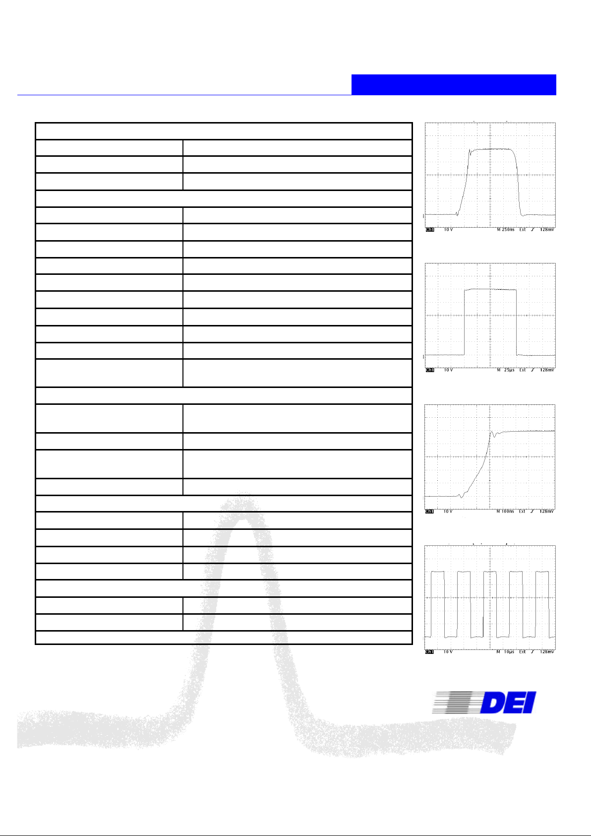
Typical 1µs Output Waveform, 50V 10A
(5Ω Load, 250ns/Div Horizontal Scale,
10V/Div Vertical Scale)
Typical 100µs Output Waveform, 50V 10A
(5Ω Load, 25µs/Div Horizontal Scale,
10V/Div Vertical Scale)
Typical Rise And Settling Times, 50V 10A
(5Ω Load, 100ns/Div Horizontal Scale,
10V/Div Vertical Scale)
50% Duty Cycle, 50KHz, 50V 10A
(5Ω Load, 10µs/Div Horizontal Scale,
10V/Div Vertical Scale)
PULSE (VHIGH) and QUIESCENT (VLOW ) PULSE VOLTAGE INPUTS
Maximum Value 75 volts DC, Floating
Minimum Value 0 volts DC
Input Connector Screw terminals, Rear Panel
OUTPUT
Maximum Value 50 volts at 10 A
Minimum Value 0 volts
Maximum Current 10 Amperes
Means of Adjustment Controlled By Pulse Input Voltage
Pulse Rise Time <200ns 50V (10%-90%)
Typical Settling Time
(1)
<400ns, including rise time
Pulse Width <1µs to 100 µs, controlled by input gate
Pulse Recurrence Frequency Single Shot to 50KHz, controlled by input gate
Maximum Duty Cycle 0.50 (50%)
Output Connector 15 pin D-sub, front panel. Pins 1-8 are pulse return
and pins 9-15 are pulse output
MONITOR OUTPUTS
Voltage Monitor 1V/V into 1MΩ, accuracy <±3% of the actual output
voltage
Voltage Monitor Connector Type BNC, Front Panel
Current Monitor 0.1V/A into 1MΩ, accuracy <±3% of the actual
output current
Current Monitor Connector Type BNC, Front Panel
CONTROL PULSE INPUT
Source External
Input Level +5V ±1V into 50Ω
Rise Time <20ns
Gate Input Connector Type BNC, Front Panel
GENERAL
Size 19” (48.25cm) W x 5.2” (13.2cm) H x 13” (33cm) D
Support Power 100-240VAC, 50/60Hz
SPECIFICATIONS SUBJECT TO CHANGE WITHOUT NOTICE
(1)
Settling time is defined as the time from the 10% point to the 99% point of the pulse. Pulsed IV data acquisition of both current and voltage waveforms is most optimum when both derivatives are at or near zero.
Therefore the data acquisition point should be set beyond the settling time of the pulse.
Doc #9200 -0218 Rev 2
© Directed Energy, Inc. 2000
 Loading...