

Page 1
MUBW15-12A6K
E72873
Converter - Brake - Inverter
Module (CBI 1)
NPT IGBT
Part name (Marking on product)
MUBW15-12A6K
Three Phase
Rectifier
V
= 1600 V V
RRM
I
= 130 A I
DAVM25
I
= 300 A V
FSM
Brake
Chopper
= 1200 V V
CES
= 19 A I
C25
= 2.9 V V
CE(sat)
Three Phase
Inverter
= 1200 V
CES
= 19 A
C25
= 2.9 V
CE(sat)
Features:
• High level of integration - only one
power semiconductor module required
for the whole drive
• Inverter with NPT IGBTs
- low saturation voltage
- positive temperature coefficient
- fast switching
- short tail current
• Epitaxial free wheeling diodes with
hiperfast and soft reverse recovery
• Industry standard package with insu
lated copper base plate and soldering
pins for PCB mounting
• Temperature sense included
Application:
AC motor drives with
• Input from single or three phase grid
• Three phase synchronous or
asynchronous motor
• Electric braking operation
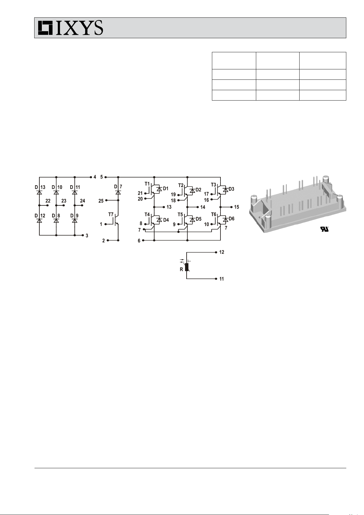
Pin configuration see outlines.
Package:
• UL registered
• Industry standard E1-pack
IXYS reserves the right to change limits, test conditions and dimensions.
© 2007 IXYS All rights reserved
20071113a
1 - 9
Page 2
MUBW15-12A6K
Ouput Inverter T1 - T6
Ratings
Symbol Definitions Conditions min. typ. max. Unit
V
CES
V
GES
V
GEM
I
C25
I
C80
P
tot
V
CE(sat)
V
GE(th)
I
CES
I
GES
C
ies
Q
G(on)
t
d(on)
t
r
t
d(off)
t
f
E
on
E
off
I
CM
t
SC
(SCSOA)
R
thJC
R
thCH
collector emitter voltage
max. DC gate voltage
max. transient collector gate voltage
collector current
total power dissipation
collector emitter saturation voltage
gate emitter threshold voltage
collector emitter leakage current
gate emitter leakage current
input capacitance
total gate charge
turn-on delay time
current rise time
turn-off delay time
current fall time
turn-on energy per pulse
turn-off energy per pulse
reverse bias safe operating area
short circuit safe operating area
thermal resistance junction to case
thermal resistance case to heatsink
TVJ = 25°C to 150°C 1200 V
continuous
transient
TC = 25°C
TC = 80°C
±20
±30
19
13
TC = 25°C 90 W
IC = 15 A; VGE = 15 V TVJ = 25°C
TVJ = 125°C
3.0
3.5
3.4 V
IC = 0.35 mA; VGE = VCE TVJ = 25°C 4.5 6.5 V
VCE = V
TVJ = 125°C 1.3
; VGE = 0 V TVJ = 25°C
CES
0.6 mA
mA
VCE = 0 V; VGE = ±20 V 100 nA
VCE = 25 V; VGE = 0 V; f = 1 MHz 600 pF
VCE = 600 V; VGE = 15 V; IC = 10 A 45 nC
inductive load TVJ = 125°C
VCE = 600 V; IC = 10 A
VGE = ±15 V; RG = 82 W
RBSOA; VGE = ±15 V; RG = 82 W
L = 100 µH;
V
CEmax
clamped induct. load
= V
- LS·di/dt
CES
TVJ = 125°C
VCE = 720 V; VGE = ±15 V; TVJ = 125°C
50
40
290
60
1.2
1.1
26 A
10 µs
ns
ns
ns
ns
mJ
mJ
RG = 82 W; non-repetitive
(per IGBT) 1.35 K/W
(per IGBT) 0.5 K/W
V
V
A
A
V
Output Inverter D1 - D6
Ratings
Symbol Definitions Conditions min. typ. max. Unit
V
RRM
I
F25
I
F80
V
F
max. repetitve reverse voltage
forward current
forward voltage
TVJ = 150°C 1200 V
TC = 25°C
T
= 80°C
C
IF = 30 A; VGE = 0 V TVJ = 25°C
26
17
3.4 V
TVJ = 125°C 2.3
I
RM
t
rr
E
rec(off)
R
thJC
R
thCH
IXYS reserves the right to change limits, test conditions and dimensions.
© 2007 IXYS All rights reserved
max. reverse recovery current
reverse recovery time
reverse recovery energy
thermal resistance junction to case
thermal resistance case to heatsink
VR = 600 V
diF /dt = -400 A/µs TVJ = 100°C
= 15 A; VGE = 0 V
IF
16
130
tbd
(per diode) 1.6 K/W
(per diode) 0.55 K/W
TC = 25°C unless otherwise stated
20071113a
2 - 9
A
A
V
A
ns
µJ
Page 3
MUBW15-12A6K
Brake Chopper T7
Ratings
Symbol Definitions Conditions min. typ. max. Unit
V
CES
V
GES
V
GEM
I
C25
I
C80
P
tot
V
CE(sat)
V
GE(th)
I
CES
I
GES
C
ies
Q
G(on)
t
d(on)
t
r
t
d(off)
t
f
E
on
E
off
I
CM
t
SC
(SCSOA)
R
thJC
R
thCH
collector emitter voltage
max. DC gate voltage
max. transient collector gate voltage
collector current
total power dissipation
collector emitter saturation voltage
gate emitter threshold voltage
collector emitter leakage current
gate emitter leakage current
input capacitance
total gate charge
turn-on delay time
current rise time
turn-off delay time
current fall time
turn-on energy per pulse
turn-off energy per pulse
reverse bias safe operating area
short circuit safe operating area
thermal resistance junction to case
thermal resistance case to heatsink
TVJ = 25°C to 150°C 1200 V
continuous
transient
TC = 25°C
TC = 80°C
±20
±30
19
13
TC = 25°C 90 W
IC = 15 A; VGE = 15 V TVJ = 25°C
TVJ = 125°C
2.9
3.5
3.4 V
IC = 0.4 mA; VGE = VCE TVJ = 25°C 4.5 6.5 V
VCE = V
TVJ = 125°C 0.8
; VGE = 0 V TVJ = 25°C
CES
0.5 mA
mA
VCE = 0 V; VGE = ±20 V 100 nA
VCE = 25 V; VGE = 0 V; f = 1 MHz 600 pF
VCE = 600 V; VGE = 15 V; IC = 10 A 45 nC
inductive load TVJ = 125°C
VCE = 600 V; IC = 10 A
VGE = ±15 V; RG = 82 W
RBSOA; VGE = ±15 V; RG = 82 W
L = 100 µH;
V
CEmax
clamped induct. load
= V
- LS·di/dt
CES
TVJ = 125°C
VCE = 720 V; VGE = ±15 V; TVJ = 125°C
45
40
290
60
1.2
1.1
20 A
10
ns
ns
ns
ns
mJ
mJ
µs
RG = 82 W; non-repetitive
(per IGBT) 1.35 K/W
(per IGBT) 0.45 K/W
V
V
A
A
V
Brake Chopper D7
Ratings
Symbol Definitions Conditions min. typ. max. Unit
V
RRM
I
F25
I
F80
V
F
max. repetitive reverse voltage
forward current
forward voltage
TVJ = 150°C 1200 V
TC = 25°C
TC = 80°C
IF = 15 A; VGE = 0 V TVJ = 25°C
15
10
3.5 V
TVJ = 125°C 2.0
I
R
reverse current
VR = V
TVJ = 25°C
RRM
0.06 mA
TVJ = 125°C 0.2
I
RM
t
rr
R
thJC
R
thCH
IXYS reserves the right to change limits, test conditions and dimensions.
© 2007 IXYS All rights reserved
max. reverse recovery current
reverse recovery time
thermal resistance junction to case
thermal resistance case to heatsink
VR = 600 V; IF = 10 A
diF /dt = -400 A/µs TVJ = 100°C
13
110
(per diode) 2.5 K/W
(per diode) 0.85 K/W
TC = 25°C unless otherwise stated
20071113a
3 - 9
A
A
V
mA
A
ns
Page 4

MUBW15-12A6K
I
V
0
R
0
Input Rectifier Bridge D8 - D13
Symbol
V
RRM
I
FAV
I
DAVM
I
FSM
P
tot
Symbol Conditions Characteristic Values
V
F
I
R
R
thJC
R
thCH
Temperature Sensor NTC
Symbol Definitions Conditions min. typ. max. Unit
R
25
B
25/85
Definitions Conditions
max. repetitive reverse voltage
average forward current
max. average DC output current
max. surge forward current
total power dissipation
forward voltage
sine 180° TC = 80°C
rectangular; d = 1/3; bridge TC = 80°C
t = 10 ms; sine 50 Hz TC = 25°C
TC = 25°C
IF = 30 A TVJ = 25°C
TVJ = 125°C
reverse current
thermal resistance junction to case
thermal resistance case to heatsink
resistance
VR = V
TVJ = 125°C 0.4
TVJ = 25°C
RRM
(per diode) TVJ = 25°C 1.4 K/W
(per diode) 0.45 K/W
TC = 25°C 4.45 4.7
Maximum Ratings
1600 V
31
89
320
80
min. typ. max.
1.0
1.35 V
1.1
0.02 mA
Ratings
5.0
3510
W
mA
kW
A
A
A
V
K
Module
Ratings
Symbol Definitions Conditions min. typ. max. Unit
T
VJ
T
VJM
T
stg
V
ISOL
M
d
d
S
d
A
Weight
operating temperature
max. virtual junction temperature
storage temperature
isolation voltage
mounting torque
creep distance on surface
strike distance through air
-40
-40
I
< 1 mA; 50/60 Hz 2500 V~
ISOL
125
150
125
°C
°C
°C
(M4) 2.0 2.2 Nm
12.7
12.7
mm
mm
40 g
Equivalent Circuits for Simulation
Ratings
Symbol Definitions Conditions min. typ. max. Unit
V
0
R
0
V
0
R
0
V
0
R
0
V
0
R
0
V
0
R
0
rectifier diode
IGBT
D8 - D13 TVJ = 125°C 0.90
T1 - T6 TVJ = 125°C 1.50
120
free wheeling diode
D1 - D6 TVJ = 125°C 1.46
31
IGBT T7 TVJ = 125°C 1.50
120
free wheeling diode D7 TVJ = 125°C 1.46
63
TC = 25°C unless otherwise stated
9
mW
mW
mW
mW
mW
V
V
V
V
V
IXYS reserves the right to change limits, test conditions and dimensions.
© 2007 IXYS All rights reserved
20071113a
4 - 9
Page 5

MUBW15-12A6K
Outline Drawing Dimensions in mm (1 mm = 0.0394“)
Product Marking
Ordering Part Name Marking on Product Delivering Mode Base Qty Ordering Code
Standard MUBW 15-12A6K MUBW15-12A6K Box 10 499 331
IXYS reserves the right to change limits, test conditions and dimensions.
© 2007 IXYS All rights reserved
20071113a
5 - 9
Page 6

MUBW15-12A6K
0.001 0.01 0.1 1
0
50
100
150
200
2 3 4 5 6 7 8 91 10
10
2
10
3
0.0 0.6 1.2 1.8 2.4
0
20
40
60
80
0 20 40 60 80
0
40
80
120
160
0 20 40 60 80 100 120 140
0.001 0.01 0.1 1 10
0.0
0.4
0.8
1.2
1.6
I2t
I
FSM
I
F
A
V
F
t
s
t
ms
P
tot
W
I
D(AV)M
A
T
amb
t
s
K/W
A
2
s
0 20 40 60 80 100 120 140
0
20
40
60
80
100
I
D(AV)
T
C
A
V
A
°C
°C
Z
thJC
T
VJ
= 125°C
T
VJ
= 25°C
TVJ= 45°C
TVJ= 150°C
50Hz, 80% V
RRM
TVJ= 45°C
TVJ= 150°C
MUBW15 -12A6K
R
thA
:
0.2 K/W
0.5 K/W
0.8 K/W
1.5 K/W
3 K/W
5 K/W
8 K/W
Fig. 1 Forward current versus
voltage drop per diode
Fig. 4 Power dissipation versus direct output current
and ambient temperature, sin 180°
Fig. 2 Surge overload current Fig. 3 I2t versus time per diode
Fig. 5 Max. forward current
vs. case temperature
Fig. 6 Transient thermal impedance junction to case
IXYS reserves the right to change limits, test conditions and dimensions.
© 2007 IXYS All rights reserved
20071113a
6 - 9
Page 7

MUBW15-12A6K
0 200 400 600 800 1000
0
10
20
30
40
50
0
40
80
120
160
200
0 1 2 3 4 5 6 7
0
5
10
15
20
25
30
0 10 20 30 40 50 60
0
5
10
15
20
0 1 2 3 4 5 6 7
0
5
10
15
20
25
30
VCE = 600V
I
C
= 10A
V
CE
V
I
C
V
CE
A
I
C
V
Q
G
-di/dt
V
V
GE
I
RM
t
rr
A/Ps
MUBW1012A7
I
RM
t
rr
9 V
11 V
A
11 V
A
4 6 8 10 12 14 16
0
5
10
15
20
25
30
VCE = 20V
V
V
GE
A
I
C
TVJ = 25°C
T
VJ
= 125°C
0 1 2 3 4
0
10
20
30
40
50
V
V
F
I
F
A
ns
nC
TVJ = 25°C
TVJ = 125°C
TVJ = 125°C
V
R
= 600 V
I
F
= 15 A
TVJ = 25°C
9 V
13 V
15 V
V
GE
= 17 V
13 V
15 V
V
GE
= 17 V
TVJ = 125°C
Fig. 7 Typ. output characteristics Fig. 8 Typ. output characteristics
Fig. 9 Typ. transfer characteristics Fig. 10 Typ. forward characteristics
of free wheeling diode
Fig. 11 Typ. turn on gate charge Fig. 12 Typ. turn off characteristics
IXYS reserves the right to change limits, test conditions and dimensions.
© 2007 IXYS All rights reserved
of free wheeling diode
20071113a
7 - 9
Page 8

MUBW15-12A6K
0 5 10 15 20
0
1
2
3
4
0
20
40
60
80
0 5 10 15 20
0
1
2
3
4
0
100
200
300
400
0.001 0.01 0.1 1 10
0.01
0.1
1
10
0 20 40 60 80 100 120 140
0.0
0.4
0.8
1.2
0
200
400
600
0 20 40 60 80 100 120 140
0.0
0.5
1.0
1.5
2.0
0
25
50
75
100
single pulse
VCE = 600V
V
GE
= ±15V
R
G
= 82:
TVJ = 125°C
V
CE
= 600V
V
GE
= ±15V
I
C
= 10A
T
VJ
= 125°C
0 200 400 600 800 1000 1200 1400
0
5
10
15
20
25
30
RG = 82 :
T
VJ
= 125°C
V
CE
= 600V
V
GE
= ±15V
RG = 82:
T
VJ
= 125°C
E
on
V
CE
= 600V
V
GE
= ±15V
I
C
= 10A
T
VJ
= 125°C
t
d(on)
t
r
E
off
t
d(off)
t
f
E
on
t
d(on)
t
r
E
off
t
d(off)
t
f
I
C
A
I
C
A
E
off
E
on
t
t
R
G
:
R
G
:
V
CE
t
s
mJ
E
on
mJ
E
off
ns
t
ns
t
I
CM
K/W
Z
thJC
V
A
mJ
ns
ns
mJ
IGBT
diode
MUBW 15-12A6K
Fig. 14 Typ. turn off energy and switching
times versus collector current
Fig.16 Typ. turn off energy and switching
times versus gate resistor
Fig. 13 Typ. turn on energy and switching
times versus collector current
Fig. 15 Typ. turn on energy and switching
times versus gate resistor
Fig. 17 Reverse biased safe operating area
RBSOA
IXYS reserves the right to change limits, test conditions and dimensions.
© 2007 IXYS All rights reserved
Fig. 18 Typ. transient thermal impedance
20071113a
8 - 9
Page 9

MUBW15-12A6K
0 1 2 3 4 5 6
0
5
10
15
20
25
V
V
CE
A
I
C
0 1 2 3 4
0
5
10
15
20
25
30
V
V
F
I
F
A
0 5 10 15 20
0
1
2
3
4
0
100
200
300
400
E
off
t
d(off)
t
f
I
C
A
E
off
t
mJ
ns
0 20 40 60 80 100 120
0.0
0.4
0.8
1.2
0
200
400
600
VCE = 600V
V
GE
= ±15V
I
C
= 20A
T
VJ
= 125°C
E
off
t
d(off)
t
f
:
E
off
t
ns
mJ
0.001 0.01 0.1 1 10
0.01
0.1
1
10
single pulse
t
s
K/W
Z
thJC
0 25 50 75 100 125 150
100
1000
10000
T
C
:
R
R
G
VCE = 600V
V
GE
= ±15V
R
G
= 82:
T
VJ
= 125°C
MUBW15-12A6K
IGBT
diode
TVJ = 25°C
TVJ = 125°C
VGE = 15V
TVJ = 125°C
TVJ = 25°C
Fig. 19 Typ. output characteristics Fig. 20 Typ. forward characteristics
Fig. 21 Typ. turn off energy and switching
times versus collector current
of free wheeling diode
Fig. 22 Typ. turn off energy and switching
times versus gate resistor
Fig. 23 Typ. transient thermal impedance Fig. 24 Typ. thermistor resistance
IXYS reserves the right to change limits, test conditions and dimensions.
© 2007 IXYS All rights reserved
versus temperature
20071113a
9 - 9
 Loading...