

查询IXTK82N25P供应商
PolarHT
TM
IXTQ 82N25P V
IXTT 82N25P I
Power MOSFET
IXTK 82N25P
N-Channel Enhancement Mode
Preliminary Data Sheet
Symbol Test Conditions Maximum Ratings
V
DSS
V
DGR
V
GSM
I
D25
I
D(RMS)
I
DM
I
AR
E
AR
E
AS
dv/dt I
P
D
T
J
T
JM
T
stg
T
L
M
d
Weight TO-3P 5.5 g
Symbol Test Conditions Characteristic Values
(TJ = 25°C, unless otherwise specified) Min. Typ. Max.
TJ= 25°C to 150°C 250 V
TJ= 25°C to 150°C; RGS = 1 MΩ 250 V
±20 V
TC= 25°C82A
External lead current limit 75 A
TC= 25°C, pulse width limited by T
JM
250 A
TC= 25°C60A
TC= 25°C40mJ
TC= 25°C 1.0 J
≤ IDM, di/dt ≤ 100 A/µs, VDD ≤ V
S
, 10 V/ns
DSS
TJ≤ 150°C, RG = 4 Ω
TC= 25°C 500 W
-55 ... +150 °C
150 °C
-55 ... +150 °C
1.6 mm (0.062 in.) from case for 10 s 300 °C
Mounting torque 1.13/10 Nm/lb.in.
TO-264 10 g
TO-268 5.0 g
= 250 V
=82 A
=35m
R
DSS
D25
DS(on)
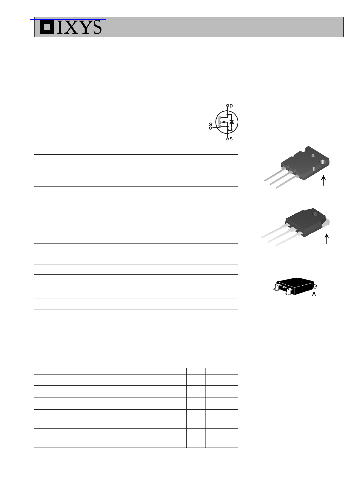
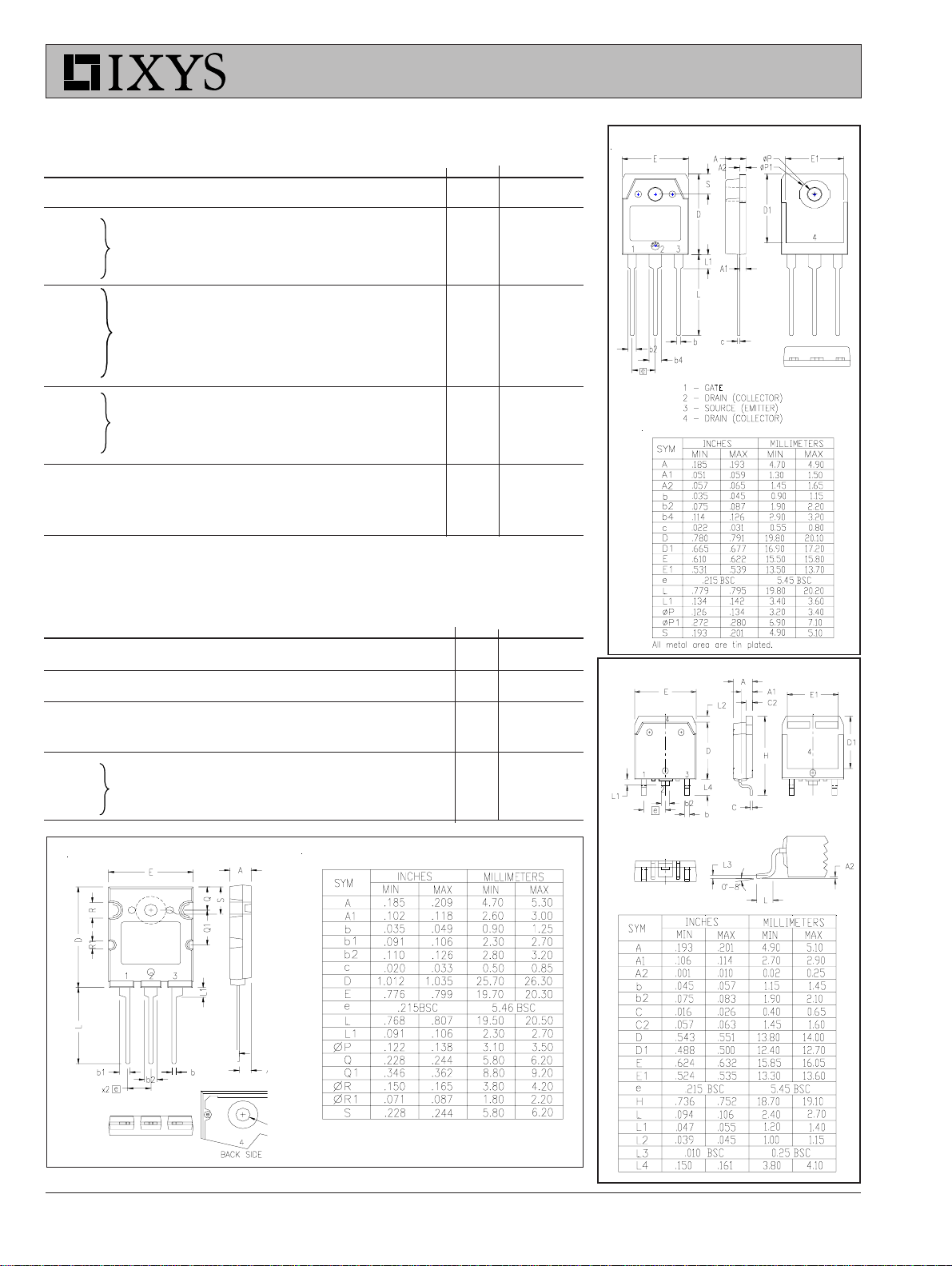
TO-264 (IXTK)
G
D
S
(TAB)
TO-3P (IXTQ)
G
D
S
(TAB)
TO-268 (IXTT)
G
S
G = Gate D = Drain
S = Source TAB = Drain
D (TAB)
Features
z
International standard packages
z
Unclamped Inductive Switching (UIS)
rated
z
Low package inductance
- easy to drive and to protect
ΩΩ
Ω
ΩΩ
V
V
I
I
DSS
GS(th)
GSS
DSS
VGS= 0 V, ID = 250 µA 250 V
VDS= VGS, ID = 250µA 2.5 5.0 V
VGS= ±20 VDC, VDS = 0 ±100 nA
VDS= V
DSS
VGS= 0 V TJ = 125°C 250 µA
R
DS(on)
VGS= 10 V, ID = 0.5 I
Pulse test, t ≤ 300 µs, duty cycle d ≤ 2 %
© 2004 IXYS All rights reserved
D25
25 µA
35 mΩ
Advantages
z
Easy to mount
z
Space savings
z
High power density
PolarHTTM DMOS transistors
utilize proprietary designs and
process. US patent is pending.
DS99121B(04/04)
IXTK 82N25P IXTQ 82N25P
IXTT 82N25P
Symbol Test Conditions Characteristic Values
= 25°C, unless otherwise specified)
J
Min. Typ. Max.
4800 pF
210 pF
29 ns
22 ns
142 nC
D25
32 nC
74 nC
0.25 K/W
g
C
C
C
t
t
t
t
Q
Q
Q
R
R
fs
iss
oss
rss
d(on)
r
d(off)
f
g(on)
gs
gd
thJC
thCH
(T
VDS= 10 V; ID = 0.5 I
, pulse test 30 52 S
D25
VGS = 0 V, VDS = 25 V, f = 1 MHz 900 pF
VGS = 10 V, VDS = 0.5 V
, ID = 60 A 20 ns
DSS
RG = 4 Ω (External) 78 ns
VGS= 10 V, VDS = 0.5 V
, ID = 0.5 I
DSS
TO-3P 0.21 K/W
TO-264 0.15 K/W
Source-Drain Diode Characteristic Values
(T
Symbol Test Conditions Min. typ. Max.
= 25°C, unless otherwise specified)
J
TO-3P Outline
I
S
I
SM
V
SD
VGS = 0 V 82 A
Repetitive 250 A
IF = IS, VGS = 0 V, 1.5 V
Pulse test, t ≤ 300 µs, duty cycle d ≤ 2 %
t
rr
IF = 25 A 200 ns
-di/dt = 100 A/µs
Q
RM
VR = 100 V 2.0 µC
TO-264 AA Outline
TO-268 Outline
IXYS reserves the right to change limits, test conditions, and dimensions.
IXYS MOSFETs and IGBTs are covered by one or more 4,850,072 4,931,844 5,034,796 5,063,307 5,237,481 5,381,025 6,404,065B1 6,162,665 6,534,343 6,583,505
of the following U.S. patents: 4,835,592 4,881,106 5,017,508 5,049,961 5,187,117 5,486,715 6,306,728B1 6,259,123B1 6,306,728B1 6,683,344

V
d
d
IXTK 82N25P IXTQ 82N25P
IXTT 82N25P
Fig. 1. Output Char acter is tics
º
@ 25
90
80
70
60
50
40
- Amperes
D
I
30
20
10
0
00.511.522.533.54
V
= 10V
GS
9V
8V
C
7V
6V
VDS - Volts
Fig. 3. Output Char acter is tics
º
90
80
70
60
50
40
- Amperes
D
I
30
20
10
0
012345678
V
= 10V
GS
9V
8V
@ 125
C
7V
6V
5V
VDS - Volts
Fig. 2. Extended Output Characteristics
@ 25
º
200
180
160
140
120
100
80
- Amperes
D
I
60
40
20
0
0 2 4 6 8 101214 1618 20
C
V
= 10V
GS
9V
8V
7V
6V
VDS - Volts
Fig . 4. R
Norm alized to I
DS(on
)
D25
vs. Junction Tem perature
2.6
2.4
2.2
1.8
1.6
1.4
- Normalize
1.2
DS( on)
R
0.8
0.6
0.4
VGS = 10V
2
I
= 82A
D
ID = 41A
1
-50 -25 0 25 50 75 100 125 150
T
- Degrees Centigrade
J
alue
Fig . 5. R
3.7
3.4
3.1
2.8
2.5
2.2
- Normalize
1.9
DS( on)
1.6
R
1.3
0.7
VGS = 10V
1
0 20 40 60 80 100 120 140 160 180 200
I
Norm alized to
DS(on)
Value vs . I
D25
ID - Amperes
T
= 125ºC
J
D
TJ = 25ºC
Fig. 6. Drain Curre nt vs. Case
90
80
70
60
50
40
- Amperes
D
I
30
20
10
0
-50 -25 0 25 50 75 100 125 150
Tem perature
T
- Degrees Centigrade
C
© 2004 IXYS All rights reserved

F
IXTK 82N25P IXTQ 82N25P
IXTT 82N25P
Fig. 7. Input Admittance
100
90
80
70
60
50
- Amperes
40
D
I
30
20
10
0
44.5 55.5 66.5 77.5 8
TJ = 125ºC
25ºC
-40ºC
VGS - Volts
Fig. 9. Sour ce Cur rent vs.
Sour ce -To-Drain Voltage
240
200
160
120
- Amperes
S
I
80
40
0
0.3 0.5 0.7 0.9 1.1 1.3 1.5
T
= 125ºC
J
T
J
= 25ºC
VSD - Volts
Fig. 8. Trans conductance
80
70
TJ = -40ºC
60
25ºC
125ºC
50
40
- Siemens
30
fs
g
20
10
0
0 20 40 60 80 100 120 140 160 180
I
- Amperes
D
Fig. 10. Gate Char ge
10
V
= 125V
DS
9
8
7
6
5
- Volts
G S
4
V
3
2
1
0
= 41A
I
D
I
= 10m A
G
0 15 30 45 60 75 90 105 120 135 150
QG - nanoCoulombs
Fig. 11. Capacitance
10000
f = 1MHz
C
iss
1000
Capacitance - p
100
0 5 10 15 20 25 30 35 40
C
oss
C
rss
VDS - Volts
1000
R
100
- Amperes
D
I
10
1
10 100 1000
Fig. 12. Forw ard-Bias
Safe Oper ating Area
Limit
DS(on )
1ms
10ms
DC
VDS - Volts
100µs
TJ = 150ºC
= 25ºC
T
C
25µs
IXYS reserves the right to change limits, test conditions, and dimensions.
IXYS MOSFETs and IGBTs are covered by one or more 4,850,072 4,931,844 5,034,796 5,063,307 5,237,481 5,381,025 6,404,065B1 6,162,665 6,534,343 6,583,505
of the following U.S. patents: 4,835,592 4,881,106 5,017,508 5,049,961 5,187,117 5,486,715 6,306,728B1 6,259,123B1 6,306,728B1 6,683,344

IXTK 82N25P IXTQ 82N25P
IXTT 82N25P
Fig. 13. M axim um Tran sien t The rm al Resistan ce
1.00
(ºC/W)
0.10
-
(th)JC
R
0.01
1 10 100 1000
Puls e W idth - millis e c ond s
© 2004 IXYS All rights reserved
 Loading...