IXYS IXTQ 180N055T Service Manual

查询IXTA180N055T供应商
Advance Technical Information
T rench Gate
Power MOSFET
IXTQ 180N055T
IXT A 180N055T
IXTP 180N055T
N-Channel Enhancement Mode
Symbol Test Conditions Maximum Ratings
V
DSS
V
DGR
V
GSM
I
D25
I
DRMS
I
DM
I
AR
E
AS
dv/dt I
TJ= 25°C to 175°C55V
TJ= 25°C to 175°C; RGS = 1 MΩ 55 V
±20 V
TC= 25°C 180 A
External lead current limit 75 A
TC= 25°C, pulse width limited by T
JM
600 A
TC= 25°C75A
TC= 25°C 1.0 J
≤ IDM, di/dt ≤ 100 A/µs, VDD ≤ V
S
, 3 V/ns
DSS
TJ≤ 150°C, RG = 10 Ω
V
DSS
I
D25
R
DS(on)
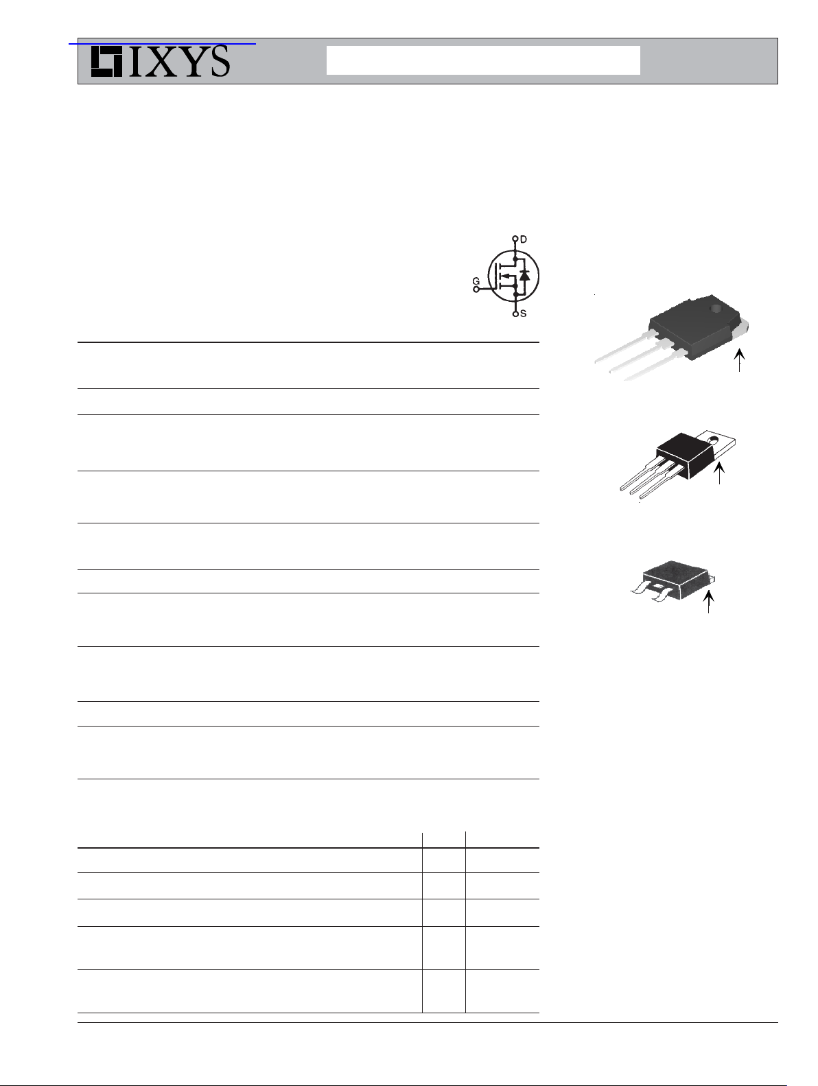
TO-3P (IXTQ)
G
D
S
TO-220 (IXTP)
G
D
TO-263 (IXTA)
= 55 V
= 180 A
(TAB)
ΩΩ
Ω
ΩΩ
(TAB)
= 4.0 m
S
P
D
T
J
T
JM
T
stg
T
L
TC= 25°C 360 W
-55 ... +175 °C
175 °C
-55 ... +150 °C
1.6 mm (0.062 in.) from case for 10 s 300 °C
Maximum tab temperature for soldering 260 °C
TO-263 package for 10s
M
d
Mounting torque (TO-3P / TO-220) 1.13/10 Nm/lb.in.
Weight TO-3P 5.5 g
TO-220 4 g
TO-263 3 g
Symbol Test Conditions Characteristic Values
(TJ = 25°C, unless otherwise specified) Min. Typ. Max.
V
V
I
I
DSS
GS(th)
GSS
DSS
VGS= 0 V, ID = 250 µA55V
VDS= VGS, ID = 1 mA 2.0 4.0 V
VGS= ±20 VDC, VDS = 0 ±200 nA
VDS= V
DSS
1 µA
VGS= 0 V TJ = 125°C 250 µA
G
S
(TAB)
G = Gate D = Drain
S = Source TAB = Drain
Features
z
International standard packages
z
Unclamped Inductive Switching (UIS)
rated
z
Low package inductance
- easy to drive and to protect
Advantages
z
Easy to mount
z
Space savings
z
High power density
R
DS(on)
VGS= 10 V, ID = 50 A 3.3 4.0 mΩ
Pulse test, t ≤ 300 µs, duty cycle d ≤ 2 %
© 2005 IXYS All rights reserved
DS99342(02/05)

IXTA 180N055T IXTP 180N055T
IXTQ 180N055T
Symbol Test Conditions Characteristic Values
(TJ = 25°C, unless otherwise specified)
Min. Typ. Max.
g
C
C
C
t
t
t
t
Q
Q
Q
R
R
fs
iss
oss
rss
d(on)
r
d(off)
f
g(on)
gs
gd
thJC
thCK
VDS= 10 V; ID = 50A, pulse test 70 90 S
5800 pF
VGS = 0 V, VDS = 25 V, f = 1 M Hz 1190 pF
138 pF
37 ns
VGS = 10 V, VDS = 40 V, ID = 40A 61 ns
RG = 5 Ω (External) 65 ns
36 ns
160 nC
VGS= 10 V, VDS = 30 V, ID = 90 A 46 nC
47 nC
0.42K/W
(TO-3P) 0.21 K/W
(TO-220) 0.25 K/W
Source-Drain Diode Characteristic Values
(T
Symbol Test Conditions Min. typ. Max.
= 25°C, unless otherwise specified)
J
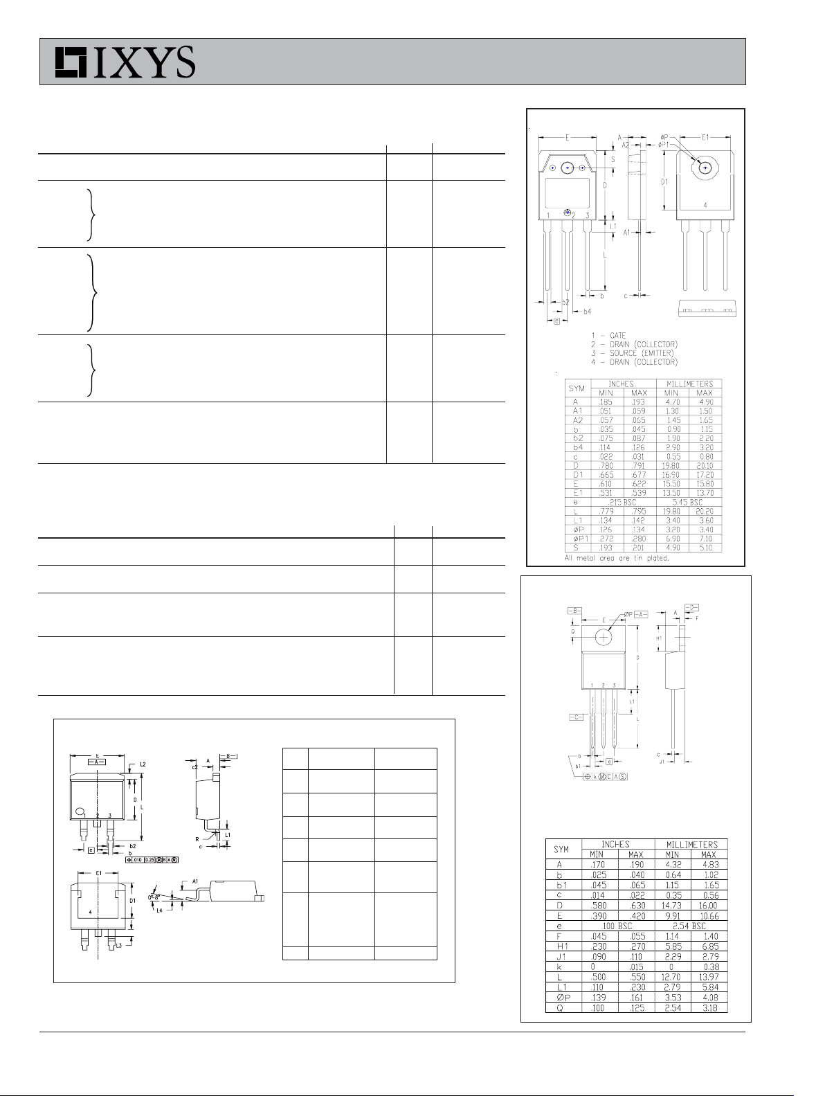
TO-3P (IXTQ) Outline
I
S
I
SM
V
SD
VGS = 0 V 180 A
Repetitive 60 0 A
IF = 50 A, VGS = 0 V, 1.2 V
Pulse test, t ≤ 300 µs, duty cycle d ≤ 2 %
t
rr
IF = 25 A 80 ns
-di/dt = 100 A/µs
Q
RM
VR = 25 V 0.4 µC
TO-263 (IXTA) Outline
Dim. Millimeter Inches
Min. Max. Min. Max.
A 4.06 4.83 .160 .190
A1 2.03 2.79 .080 .110
b 0.51 0.99 .020 .039
b2 1.14 1.40 .045 .055
c 0.46 0.74 .018 .029
c2 1.14 1.40 .045 .055
D 8.64 9.65 .340 .380
D1 7.11 8.13 .280 .320
E 9.65 10.29 .380 .405
E1 6.86 8.13 .270 .320
e 2.54 BSC .100 BSC
L 14.61 15.88 .575 .625
L1 2.29 2.79 .090 .110
L2 1.02 1.40 .040 .055
L3 1.27 1.78 .050 .070
L4 0 0.38 0 .015
R 0.46 0.74 .018 .029
TO-220 (IXTP) Outline
Pins: 1 - Gate 2 - Drain
IXYS reserves the right to change limits, test conditions, and dimensions.
IXYS MOSFETs and IGBTs are covered by 4,835,592 4,931,844 5,049,961 5,237,481 6,162,665 6,404,065 B1 6,683,344 6,727,585
one or moreof the following U.S. patents: 4,850,072 5,017,508 5,063,307 5,381,025 6,259,123 B1 6,534,343 6,710,405B2 6,759,692
4,881,106 5,034,796 5,187,117 5,486,715 6,306,728 B1 6,583,505 6,710,463
 Loading...