

TrenchMV
TM
Power MOSFET
IXTA80N10T
IXTP80N10T
V
I
DSS
D25
= 100V
= 80A
N-Channel Enhancement Mode
Avalanche Rated
Fast Intrinsic Diode
Symbol Test Conditions Maximum Ratings
V
DSS
V
DGR
V
GSS
V
GSM
I
D25
I
DM
I
A
E
AS
P
D
dV/dt IS≤ IDM, VDD ≤ V
T
J
T
JM
T
stg
T
L
T
SOLD
M
d
Weight TO-263 2.5 g
TO-220 3.0 g
TJ= 25°C to 175°C 100 V
TJ= 25°C to 175°C, RGS = 1MΩ 100 V
Continuous ± 20 V
Transient ± 30 V
TC= 25°C 80 A
TC= 25°C, Pulse Width Limited by T
JM
220 A
TC= 25°C25A
TC= 25°C 400 mJ
TC= 25°C 230 W
, TJ ≤ 175°C 10 V/ns
DSS
-55 ... +175 °C
175 °C
-55 ... +175 °C
1.6mm (0.062 in.) from Case for 10s 300 °C
Plastic Body for 10s 260 °C
Mounting Torque (TO-220) 1.13 / 10 Nm/lb.in.
R
DS(on)
≤≤
≤ 14m
≤≤
ΩΩ
Ω
ΩΩ
TO-263 AA (IXTA)
G
S
D (Tab)
TO-220AB (IXTP)
G
D
G = Gate D = Drain
S = Source Tab = Drain
D (Tab)
S
Features
z
International Standard Packages
z
175°C Operating Temperature
z
Avalanche Rated
z
High Current Handling Capability
z
Fast Intrinsic Diode
z
Low R
DS(on)
Advantages
Symbol Test Conditions Characteristic Values
(TJ = 25°C Unless Otherwise Specified) Min. Typ. Max.
BV
V
I
GSS
I
DSS
DSS
GS(th)
VGS= 0V, ID = 250μA 105 V
VDS= VGS, ID = 100μA 2.5 5.0 V
VGS= ± 20V, VDS = 0V ± 200 nA
VDS= 105V, VGS= 0V 5 μA
TJ = 150°C 150 μA
R
DS(on)
© 2009 IXYS CORPORATION, All Rights Reserved
VGS= 10V, ID = 25A, Note 1 & 2 14 mΩ
z
Easy to Mount
z
Space Savings
z
High Power Density
Applications
z
Automotive
- Motor Drives
- DC/DC Conversion
- 42V Power Bus
- ABS Systems
z
DC/DC Converters and Off-Line UPS
z
Primary Switch for 24V and 48V
Systems
z
High Current Switching Applications
z
Distributed Power Architechtures
and VRMs
z
Electronic Valve Train Systems
DS99648A(11/09)
Symbol Test Conditions Characteristic Values
(TJ = 25°C Unless Otherwise Specified) Min. Typ. Max.
g
C
C
C
t
d(on)
t
r
t
d(off)
t
f
Q
Q
Q
R
R
fs
iss
oss
rss
g(on)
gs
gd
thJC
thCS
V
= 10V, ID = 0.5 • I
DS
, Note 1 33 55 S
D25
3040 pF
VGS = 0V, VDS = 25V, f = 1MHz 420 pF
90 pF
31 ns
Resistive Switching Times
54 ns
= 10V, VDS = 0.5 • V
V
GS
40 ns
RG = 15Ω (External)
, ID = 10A
DSS
48 ns
60 nC
V
= 10V, VDS = 0.5 • V
GS
, ID = 25A 21 nC
DSS
15 nC
0.65 °C/W
0.50 °C/W
Source-Drain Diode
IXTA80N10T
IXTP80N10T
TO-263 (IXTA) Outline
1. Gate
2. Drain
3. Source
Dim. Millimeter Inches
Min. Max. Min. Max.
A 4.06 4.83 .160 .190
b 0.51 0.99 .020 .039
b2 1.14 1.40 .045 .055
c 0.40 0.74 .016 .029
c2 1.14 1.40 .045 .055
D 8.64 9.65 .340 .380
D1 8.00 8.89 .280 .320
E 9.65 10.41 .380 .405
E1 6.22 8.13 .270 .320
e 2.54 BSC .100 BSC
L 14.61 15.88 .575 .625
L1 2.29 2.79 .090 .110
L2 1.02 1.40 .040 .055
L3 1.27 1.78 .050 .070
L4 0 0.13 0 .005
Symbol Test Conditions Characteristic Values
(TJ = 25°C, Unless Otherwise Specified) Min. Typ. Max.
I
S
I
SM
V
SD
t
rr
VGS= 0V 80 A
Repetitive, Pulse Width Limited by T
JM
220 A
IF = 25A, VGS = 0V, Note 1 1.1 V
IF = 25A, -di/dt = 100A/μs
V
= 50V, VGS = 0V
R
100 ns
Notes 1. Pulse test, t ≤ 300μs, duty cycle, d ≤ 2%.
2. On through-kole packages R
Kelvin test contact location
DS(on)
must be 5 mm or less from the package body.
TO-220 (IXTP) Outline
Pins: 1 - Gate 2 - Drain
3 - Source 4 - Drain
IXYS Reserves the Right to Change Limits, Test Conditions, and Dimensions.
IXYS MOSFETs and IGBTs are covered 4,835,592 4,931,844 5,049,961 5,237,481 6,162,665 6,404,065 B1 6,683,344 6,727,585 7,005,734 B2 7,157,338B2
by one or more of the following U.S. patents: 4,850,072 5,017,508 5,063,307 5,381,025 6,259,123 B1 6,534,343 6,710,405 B2 6,759,692 7,063,975 B2
4,881,106 5,034,796 5,187,117 5,486,715 6,306,728 B1 6,583,505 6,710,463 6,771,478 B2 7,071,537

IXTA80N10T
IXTP80N10T
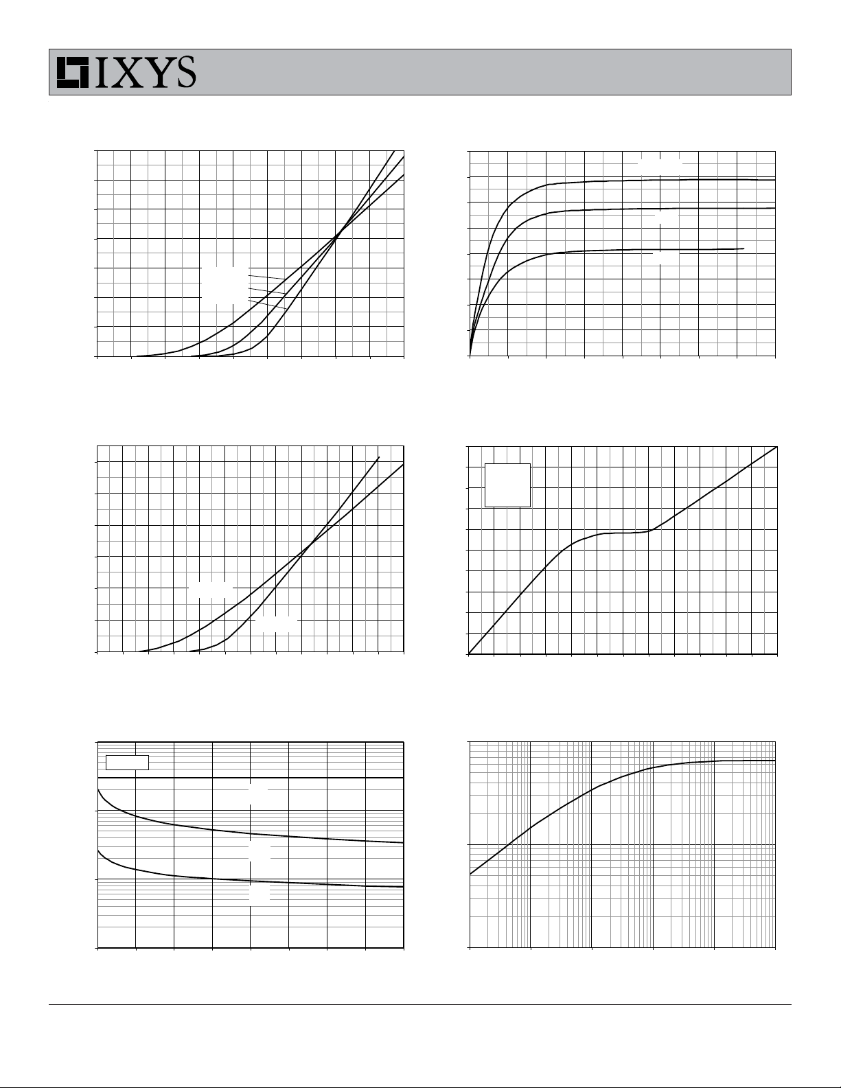
Fig. 1. Ou tp u t C h ar acter i sti cs @ TJ = 25ºC
80
70
60
50
40
- Amperes
D
I
30
20
10
0
0.0 0.1 0.2 0.3 0.4 0.5 0.6 0.7 0.8 0.9 1.0 1.1 1.2
VDS - Volts
V
= 10V
GS
9V
8V
7V
6V
Fig. 3. Ou tp u t C h ar acter i sti cs @ TJ = 150ºC
- Amperes
D
I
80
70
60
50
40
30
20
10
V
GS
9V
8V
= 10V
7V
6V
5V
Fig. 2. Extended Output Characteristics @ TJ = 25ºC
280
V
= 10V
240
200
160
- Amperes
120
D
I
80
40
0
0 2 4 6 8 10 12 14 16 18 20
GS
9V
8V
7V
6V
VDS - Volts
Fig. 4. R
Normalized to ID = 40A Value vs.
DS(on)
Junction Temperature
2.8
V
= 10V
GS
2.4
- Normalized
DS(on)
R
2.0
1.6
1.2
0.8
I D = 80A
I D = 40A
0
0.0 0.2 0.4 0.6 0.8 1.0 1.2 1.4 1.6 1.8 2.0 2.2 2.4
VDS - Volts
Fig. 5. R
Normalized to ID = 40A Value
DS(on)
vs. Drain C u r r en t
4.6
4.2
V
= 10V
GS
15V
3.8
3.4
3.0
2.6
- Normalized
2.2
DS(on)
R
1.8
1.4
1.0
0.6
0 25 50 75 100 125 150 175 200 225 250
- - - -
ID - Amperes
© 2009 IXYS CORPORATION, All Rights Reserved
TJ = 175ºC
TJ = 25ºC
0.4
-50 -25 0 25 50 75 100 125 150 175
TJ - Degrees Centigrade
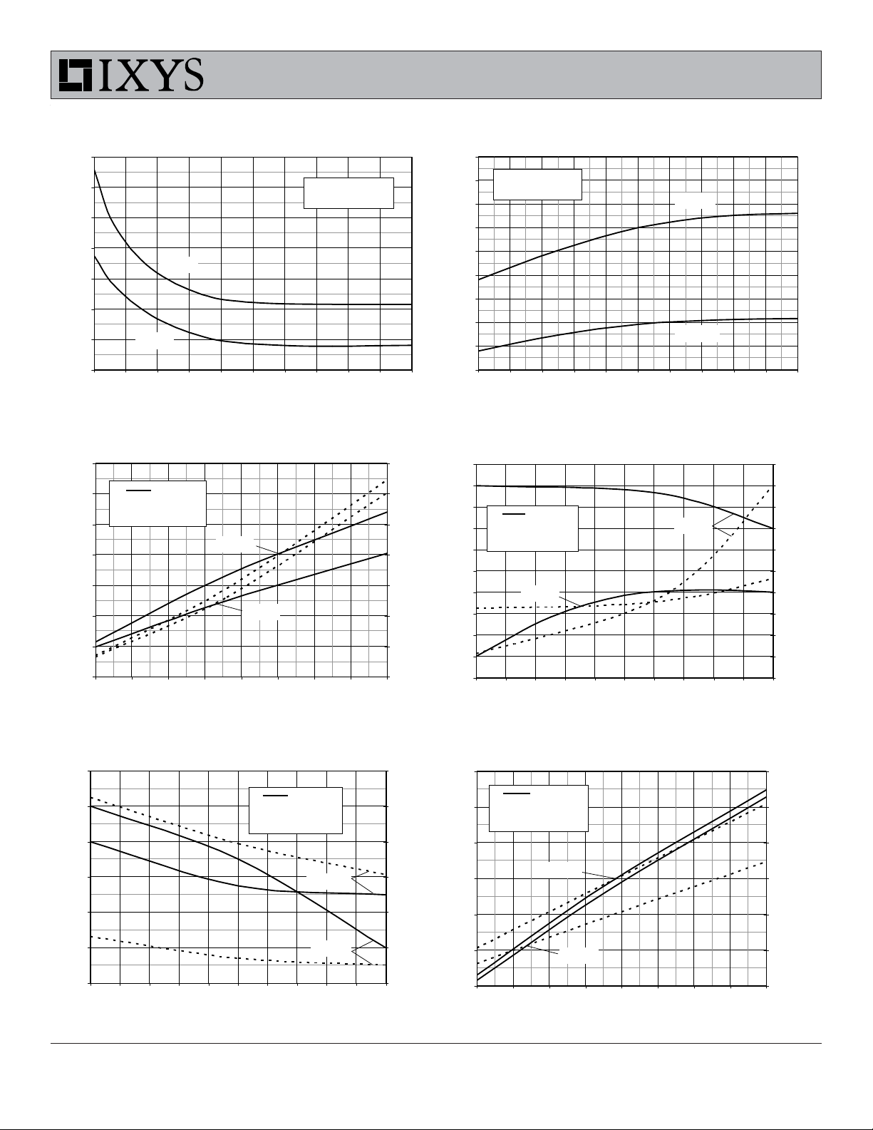
Fig. 6. D r ai n C u r r en t vs. C ase Temp er atu r e
90
80
70
60
50
40
- Amperes
D
I
30
20
10
0
-50 -25 0 25 50 75 100 125 150 175
TC - Degrees Centigrade
IXTA80N10T
IXTP80N10T
Fig. 7. Input Admittance
140
120
100
80
- Amperes
60
D
I
40
20
0
3.5 4.0 4. 5 5.0 5.5 6.0 6. 5 7.0 7.5 8.0
T
= 150ºC
J
25ºC
- 40ºC
VGS - Volts
Fig. 9. Forward Voltage Drop of
Intri n si c D i o d e
240
200
160
120
- Amperes
S
I
80
40
0
0.3 0.4 0.5 0.6 0.7 0.8 0. 9 1 1.1 1.2 1.3 1.4 1.5
T
J
= 150ºC
TJ = 25ºC
VSD - Volts
Fig. 8. Transconductance
80
T
= - 40ºC
70
60
50
40
- Siemens
f s
30
g
20
10
0
0 20406080100120140160
J
25ºC
150ºC
ID - Amperes
Fig. 10. Gate Charge
10
9
V
= 50V
DS
= 25A
I
D
8
= 10mA
I
G
7
6
5
- Volts
GS
V
4
3
2
1
0
0 5 10 15 20 25 30 35 40 45 50 55 60
QG - NanoCoulombs
Fig. 11. Capacitance
10,000
f = 1 MHz
C
1,000
100
Capacitance - PicoFarads
10
0 5 10 15 20 25 30 35 40
iss
C
oss
C
rss
VDS - Volts
IXYS Reserves the Right to Change Limits, Test Conditions, and Dimensions.
Fig. 12. Maximum Transient Thermal Impedance
1.00
- ºC / W
0.10
(th)JC
Z
0.01
0.0001 0.001 0.01 0.1 1 10
Pulse Width - Sec onds
IXTA80N10T
(
)
(
)
(
)
(
)
IXTP80N10T
Fig. 1 3. R esistive Tu rn-on
Rise Time vs. Junction Temp er a tu r e
70
R
= 15
VGS = 10V
65
60
55
50
- Nanoseconds
r
t
45
40
35
25 35 45 55 65 75 85 95 105 115 125
I D = 30A
I D = 10A
G
V
DS
= 50V
,
TJ - De grees Centigrade
Fig. 15. Resistive Turn-o n
Switchin g Times vs. Gate Resistan c e
280
t
r
240
TJ = 125ºC, VGS = 10V
V
= 50V
DS
80
40
0
15 20 25 30 35 40 45 50 55
- Nanoseconds
r
t
200
160
120
t
d(on)
- - - -
I D = 30A
I D = 10A
RG - Ohms
Fig. 14. Resistive Turn-on
Rise T i me vs. Dr ai n C urrent
80
R
= 15 , VGS = 10V
G
75
V
= 50V
DS
70
65
60
55
- Nanoseconds
r
t
50
45
40
35
10 12 14 16 18 20 22 24 26 28 30
TJ = 25ºC
TJ = 125ºC
ID - Amperes
Fig. 16. Resistive Turn-o ff
Switchin g Times vs. Junction Temperature
95
85
t
d
75
o n
- Nanoseconds
65
55
45
35
25
49
48
47
t
f
46
RG = 15, VGS = 10V
V
= 50V
DS
45
44
43
- Nanoseconds
f
t
42
41
40
39
25 35 45 55 65 75 85 95 105 115 125
t
d(off)
I D = 30A
- - - -
I D = 10A
TJ - Degrees C entigr ade
76
72
68
t
d
o f f
64
60
- Nanoseconds
56
52
48
44
40
36
Fig. 1 7. R esistive Tu rn-off
Switchin g Times vs. Dr ain Curr ent
50
t
48
46
44
- Nanoseconds
42
f
t
40
38
10 12 14 16 18 20 22 24 26 28 30
f
RG = 15, VGS = 10V
V
= 50V
DS
t
- - - -
d(off)
TJ = 125ºC
TJ = 25ºC
ID - Amperes
78
70
d
o f f
62
160
t
f
140
t
TJ = 125ºC, VGS = 10V
V
DS
120
- Nanoseconds
54
46
38
30
100
- Nanoseconds
f
80
t
60
40
15 20 25 30 35 40 45 50 55
© 2009 IXYS CORPORATION, All Rights Reserved
Fig. 18. Re sis ti ve Turn-o ff
Switchin g Tim es vs. Gate R esi stan ce
t
- - - -
d(off)
= 50V
I D = 10A
I D = 30A
RG - Ohms
270
230
t
d
o f f
190
- Nanoseconds
150
110
70
30
IXYS REF: T_80N10T(3V)12-11-07-A
 Loading...