IXYS IXTH1N100, IXTT1N100 Datasheet

Advance Technical Information
High V oltage MOSFET
IXTH 1N100
IXTT 1N100
N-Channel Enhancement Mode
Avalanche Energy Rated
Symbol Test Conditions Maximum Ratings
V
DSS
V
DGR
V
GS
V
GSM
I
D25
I
DM
I
AR
E
AR
E
AS
dv/dt I
P
D
T
J
T
JM
T
stg
M
d
Weight TO-268 4 g
Maximum lead temperature for soldering 30 0 °C
1.6 mm (0.062 in.) from case for 10 s
TJ= 25°C to 150°C 1000 V
TJ= 25°C to 150°C; RGS = 1 MΩ 1000 V
Continuous ±20 V
Transient ±30 V
TC= 25°C 1.5 A
TC= 25°C, pulse width limited by T
TC= 25°C6mJ
TC= 25°C 200 mJ
≤ IDM, di/dt ≤ 100 A/µs, VDD ≤ V
S
T
≤ 150°C, RG = 18 Ω
J
TC= 25°C60W
Mounting torque (TO-247) 1.13/10 Nm/lb.in.
TO-247 6 g
JM
, 3 V/ns
DSS
-55 ... +150 °C
-55 ... +150 °C
6A
1.5 A
150 °C
V
DSS
I
D25
R
DS(on)
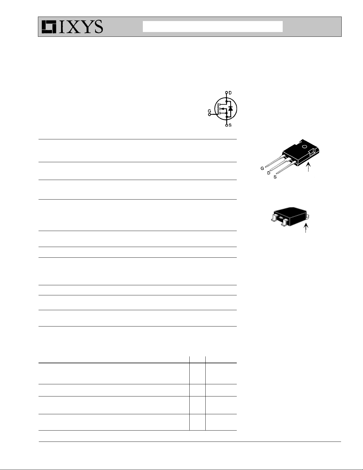
TO-247 AD (IXTH)
TO-268 Case Style
G
G = Gate, D = Drain,
S = Source, TAB = Drain
Features
= 1000 V
= 1.5 A
= 11
S
D (TAB)
(TAB)
ΩΩ
Ω
ΩΩ
International standard packages
High voltage, Low R
process
DS (on)
HDMOS
TM
Rugged polysilicon gate cell structure
Fast switching times
Symbol Test Conditions Characteristic Values
(TJ = 25°C, unless otherwise specified)
min. typ. max.
V
DSS
V
GS(th)
I
GSS
I
DSS
R
DS(on)
© 2002 IXYS All rights reserved
VGS= 0 V, ID = 250 µA 1000 V
VDS= VGS, ID = 25 µA 2.5 4.5 V
VGS= ±20 VDC, VDS = 0 ±100 nA
VDS= V
VGS= 0 V TJ = 125°C 500 µA
VGS= 10 V, ID = 1.0A 11 Ω
Pulse test, t ≤ 300 µs, duty cycle d ≤ 2 %
DSS
TJ = 25°C25µA
Applications
Switch-mode and resonant-mode
power supplies
Flyback inverters
DC choppers
High frequency matching
Advantages
Space savings
High power density
98886 (1/2)

IXTH 1N100
IXTT 1N100
Symbol Test Conditions Characteristic Values
= 25°C, unless otherwise specified)
(T
g
C
C
C
t
t
t
t
Q
Q
Q
R
R
fs
iss
oss
rss
d(on)
r
d(off)
f
g(on)
gs
gd
thJC
thCK
J
VDS= 20 V; ID = 1.0A, pulse test 0.8 1.5 S
VGS= 0 V, VDS = 25 V, f = 1 MHz 45 pF
VGS= 10 V, VDS = 0.5 • V
, ID = 1A 19 ns
DSS
RG= 18Ω, (External) 20 ns
VGS= 10 V, VDS = 0.5 • V
, ID = 1A 4.5 nC
DSS
TO-247 0.25 K/W
min. typ. max.
480 pF
15 pF
18 ns
18 ns
23 nC
14 nC
2.3 K/W
Source-Drain Diode Characteristic Values
(TJ = 25°C, unless otherwise specified)
Symbol Test Conditions min. typ. max.
I
S
I
SM
V
SD
VGS= 0 V 1.5 A
Repetitive; pulse width limited by T
JM
6A
IF = IS, VGS = 0 V, 1.8 V
Pulse test, t ≤ 300 µs, duty cycle d ≤ 2 %
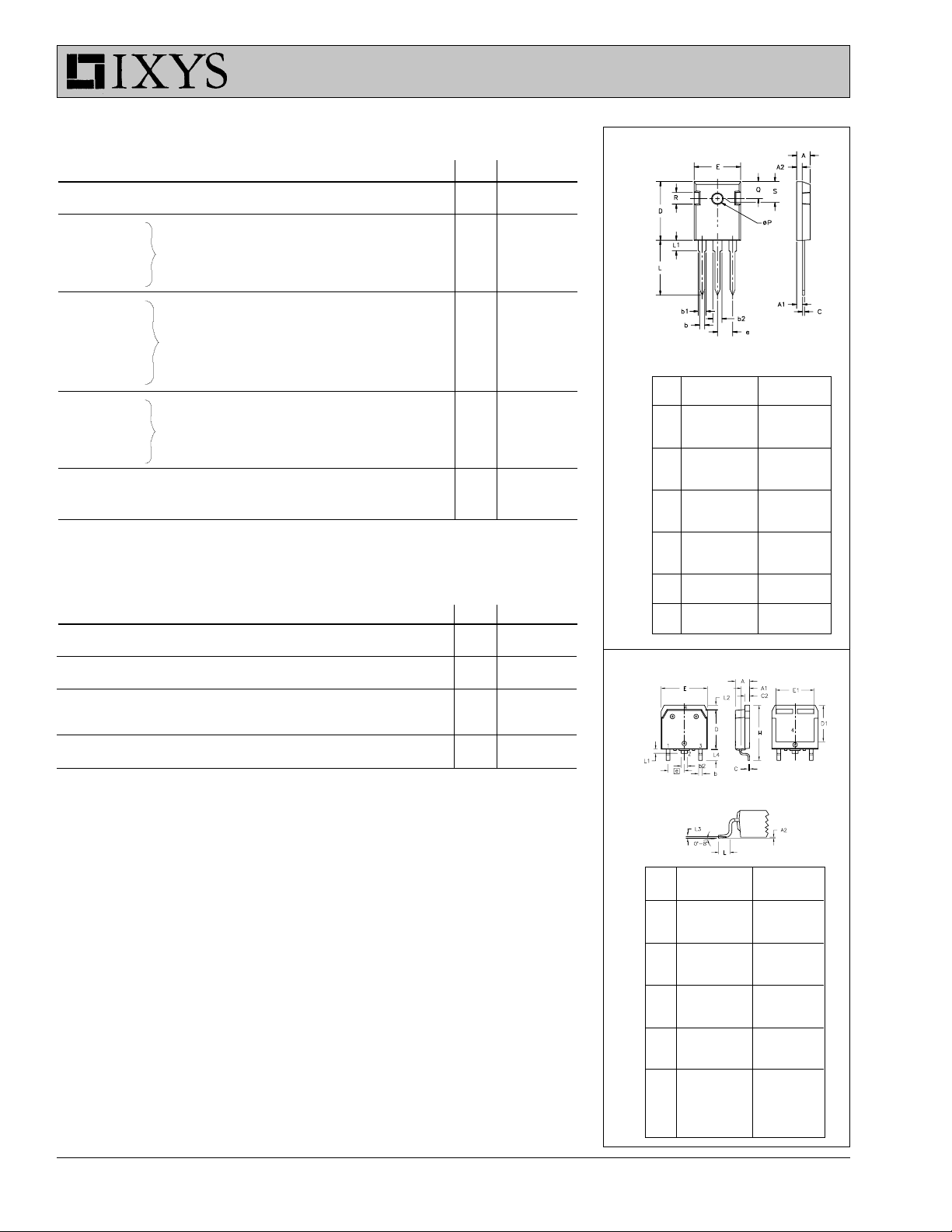
TO-247 AD Outline
1 2 3
Terminals: 1 - Gate 2 - Drain
3 - Source Tab - Drain
Dim. Millimeter Inches
Min. Max. Min. Max.
A 4.7 5.3 .185 .209
A
2.2 2.54 .087 .102
1
A
2.2 2.6 .059 .098
2
b 1.0 1.4 .040 .055
b
1.65 2.13 .065 .084
1
b22.87 3.12 .113 .123
C .4 .8 .016 .031
D 20.80 21.46 .819 .845
E 15.75 16.26 .610 .640
e 5.20 5.72 0.205 0.225
L 19.81 20.32 .780 .800
L1 4.50 .177
ÆP 3.55 3.65 .140 .144
Q 5.89 6.40 0.232 0.252
R 4.32 5.49 .170 .216
S 6.15 BSC 242 BSC
TO-268 Outline
t
rr
IF = IS, -di/dt = 100 A/µs, VR = 100 V 710 ns
Dim. Millimeter Inches
Min. Max. Min. Max.
A 4.9 5.1 .193 .201
A
2.7 2.9 .106 .114
1
A2.02 .25 .001 .010
b 1.15 1.45 .045 .057
b
1.9 2.1 .75 .83
2
C .4 .65 .016 .026
D 13.80 14.00 .543 .551
E 15.85 16.05 .624 .632
13.3 13.6 .524 .535
E
1
e 5.45 BSC .215 BSC
H 18.70 19.10 .736 .752
L 2.40 2.70 .094 .106
L1 1.20 1.40 .047 .055
L2 1.00 1.15 .039 .045
L3 0.25 BSC .010 BSC
L4 3.80 4.10 .150 .161
IXYS reserves the right to change limits, test conditions, and dimensions.
IXYS MOSFETS and IGBTs are covered by one or more of the following U.S. patents: 4,835,592 4,881,106 5,017,508 5,049,961 5,187,117 5,486,715 6,306,728B1
4,850,072 4,931,844 5,034,796 5,063,307 5,237,481 5,381,025
 Loading...