IXYS IXTC13N50 Datasheet

ADVANCE TECHNICAL INFORMATION
Power MOSFET IXTC 13N50 V
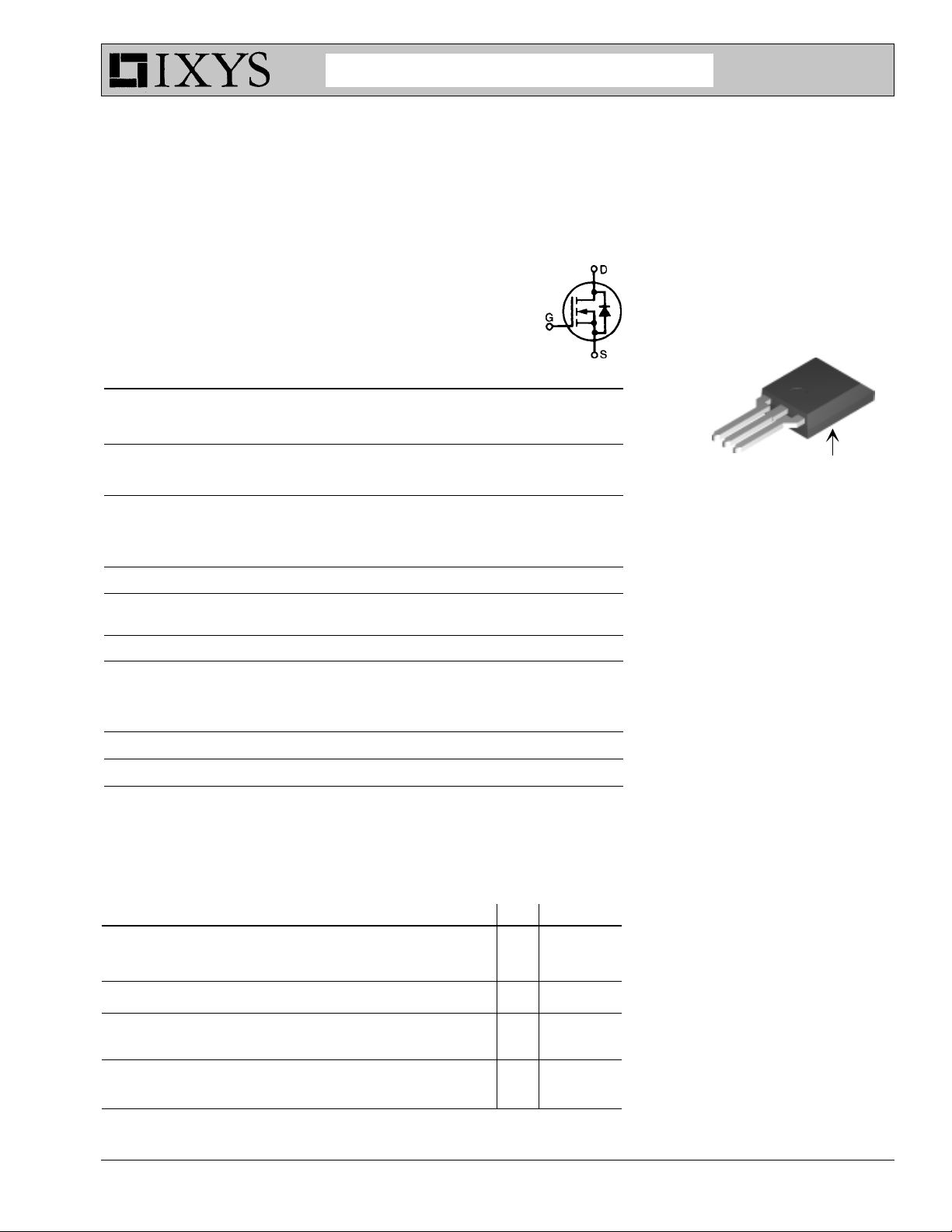
ISOPLUS220
Electrically Isolated Back Surface R
N-Channel Enhancement Mode
High dv/dt, Low t
Symbol Test Conditions Maximum Ratings
V
DSS
V
DGR
V
GS
V
GSM
I
D25
I
DM
I
AR
E
AR
dv/dt I
P
D
T
J
T
JM
T
stg
T
L
Weight 3g
T
= 25°C to 150°C 500 V
J
T
= 25°C to 150°C; RGS = 1 MΩ 500 V
J
Continuous ±20 V
Transient ±30 V
T
= 25°C12A
C
T
= 25°C, pulse width limited by T
C
T
= 25°C13A
C
T
= 25°C18mJ
C
≤ IDM, di/dt ≤ 100 A/µs, VDD ≤ V
S
T
≤ 150°C, RG = 2 Ω
J
T
= 25°C 140 W
C
1.6 mm (0.062 in.) from case for 10 s 300 °C
TM
, HDMOSTM Family
rr
JM
, 5 V/ns
DSS
48 A
-55 ... +150 °C
150 °C
-55 ... +150 °C
I
ISOPLUS 220
G = Gate, D = Drain,
S = Source
* Patent pending
Features
l
Silicon chip on Direct-Copper-Bond
substrate
- High power dissipation
- Isolated mounting surface
- 2500V electrical isolation
l
Low drain to tab capacitance(<35pF)
l
Low R
l
Rugged polysilicon gate cell structure
l
Unclamped Inductive Switching (UIS)
rated
DSS
D25
DS(on)
= 500 V
= 12 A
= 0.4
TM
G
D
S
DS (on)
Isolated back surface*
HDMOSTM process
Ω Ω
Ω
Ω Ω
Symbol Test Conditions Characteristic Values
(T
= 25°C, unless otherwise specified)
V
DSS
V
GS(th)
I
GSS
I
DSS
R
DS(on)
© 2001 IXYS All rights reserved
VGS= 0 V, I
D
VDS= VGS, ID = 2.5 mA 2 4 V
V
= ±20 V
GS
DC
VDS= 0.8 V
VGS= 0 V T
VGS= 10 V, ID = I
Notes 1, 2
J
= 250 µA 500 V
, V
= 0 ±100 nA
DS
T
DSS
T
= 25°C 200 µA
J
= 125°C1mA
J
min. typ. max.
0.4 Ω
Applications
l
DC-DC converters
l
Battery chargers
l
Switched-mode and resonant-mode
power supplies
l
DC choppers
l
AC motor control
Advantages
l
Easy assembly: no screws or isolation
foils required
l
Space savings
l
High power density
l
Low collector capacitance to ground
(low EMI)
98823 (05/01)

IXTC 13N50
Symbol Test Conditions Characteristic Values
(T
= 25°C, unless otherwise specified)
g
C
C
C
t
t
t
t
Q
Q
Q
R
R
fs
iss
oss
rss
d(on)
r
d(off)
f
g(on)
gs
gd
thJC
thCK
J
VDS= 10 V; ID = 0; IT Notes 1, 2 7.5 9.0 S
VGS= 0 V, VDS = 25 V, f = 1 MHz 300 pF
VGS= 10 V, VDS = 0.5 V
ID = 0.5 I
, R
= 4.7 Ω (External) 76 100 ns
D25
G
VGS= 10 V, VDS = 0.5 V
,2740ns
DSS
, ID = I
DSS
min. typ. max.
2800 pF
T
0.30 K/W
70 pF
18 30 ns
32 60 ns
110 120 nC
15 25 nC
40 50 nC
0.90 K/W
Source-Drain Diode Characteristic Values
(T
= 25°C, unless otherwise specified)
Symbol Test Conditions min. typ. max.
I
S
I
SM
V
SD
t
rr
VGS= 0 V 13 A
Repetitive; pulse width limited by T
IF = IS, VGS = 0 V, 1.5 V
Note 1
IF = I
S
-di/dt = 100 A/µs,
J
JM
52 A
600 ns
VR = 100 V
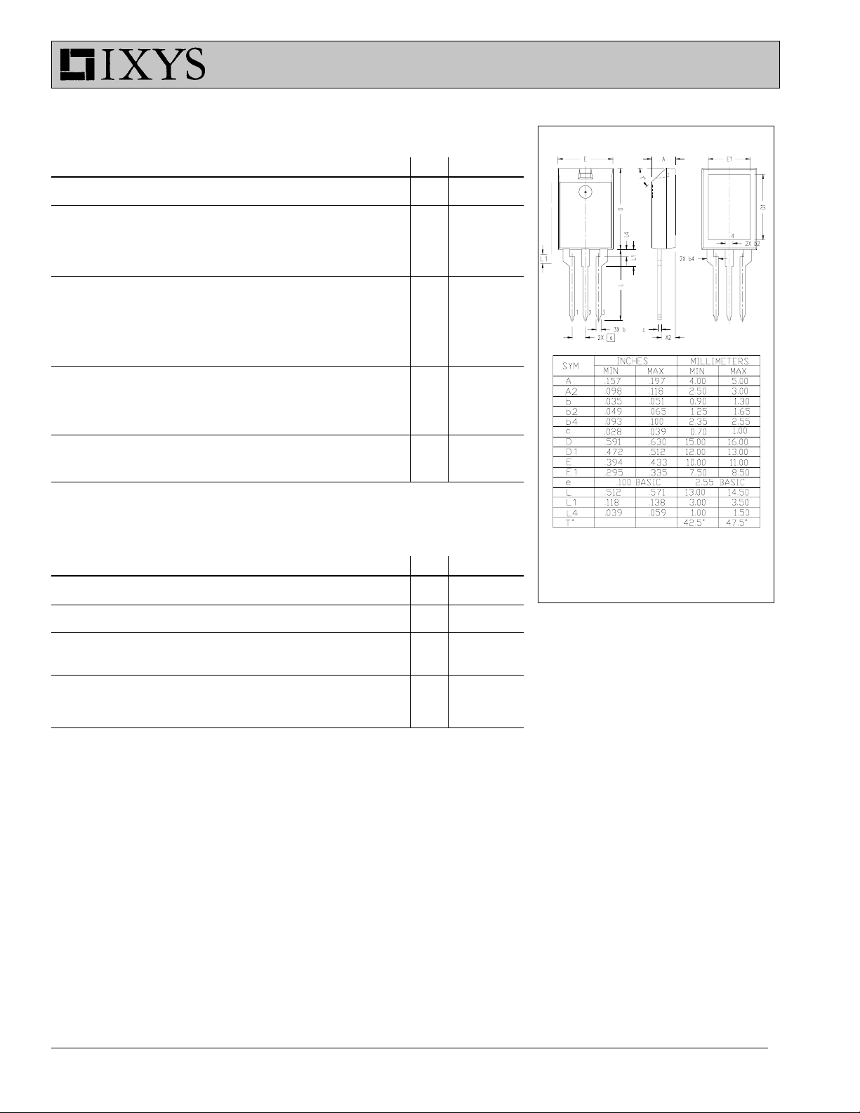
ISOPLUS220 OUTLINE
Note: All terminals are solder plated.
1 - Gate
2 - Drain
3 - Source
Note: 1. Pulse test, t ≤ 300 µs, duty cycle d ≤ 2 %
2. IT test current: IT = 6.5A
3. See IXTH12N50A data sheet for characteristic curves.
IXYS reserves the right to change limits, test conditions, and dimensions.
IXYS MOSFETS and IGBTs are covered by one or more of the following U.S. patents: 4,835,592 4,881,106 5,017,508 5,049,961 5,187,117 5,486,715
4,850,072 4,931,844 5,034,796 5,063,307 5,237,481 5,381,025
 Loading...