

查询IXTA5N50P供应商查询IXTA5N50P供应商
Advance Technical Information
PolarHV
TM
Power MOSFET
IXTA 5N50P
IXTP 5N50P
IXTY 5N50P
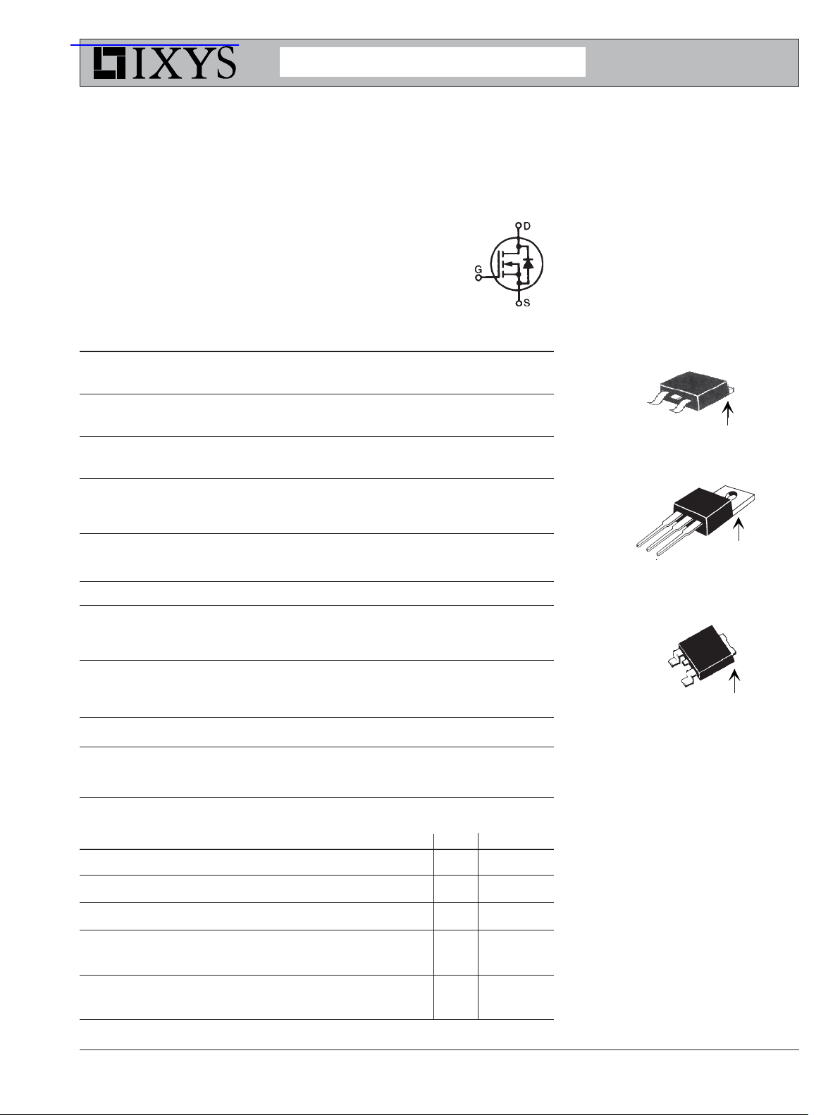
N-Channel Enhancement Mode
Symbol Test Conditions Maximum Ratings
V
DSS
V
DGR
Continuous ± 30 V
V
GSS
V
GSM
I
D25
I
DM
I
AR
E
AR
E
AS
TJ= 25°C to 150°C 500 V
TJ= 25°C to 150°C; RGS = 1 MΩ 500 V
Transient ± 40 V
TC= 25°C 4.8 A
TC= 25°C, pulse width limited by T
JM
10 A
TC= 25°C5A
TC= 25°C20mJ
TC= 25°C 250 mJ
V
DSS
I
D25
R
DS(on)
TO-263 (IXTA)
TO-220 (IXTP)
= 500 V
= 4.8 A
≤≤
≤ 1.4
≤≤
G
S
(TAB)
ΩΩ
Ω
ΩΩ
dv/dt I
≤ IDM, di/dt ≤ 100 A/μs, VDD ≤ V
S
, 10 V/ns
DSS
TJ≤ 150°C, RG = 20 Ω
P
D
T
J
T
JM
T
stg
T
L
TC= 25°C89W
-55 ... +150 °C
150 °C
-55 ... +150 °C
1.6 mm (0.062 in.) from case for 10 s 300 °C
Maximum tab temperature for soldering 260 °C
TO-263 package for 10s
M
d
Mounting torque (TO-220) 1.13/10 Nm/lb.in.
Weight TO-220 4 g
TO-263 3 g
TO-252 0.8 g
Symbol Test Conditions Characteristic Values
(TJ = 25°C, unless otherwise specified) Min. Typ. Max.
V
V
I
I
DSS
GS(th)
GSS
DSS
VGS= 0 V, ID = 250 μA 500 V
VDS= VGS, ID = 50μA 3.0 5.0 V
VGS= ±30 VDC, VDS = 0 ±100 nA
VDS= V
DSS
5 μA
VGS= 0 V TJ = 125°C50μA
R
DS(on)
VGS= 10 V, ID = 0.5 I
D25
1.4 Ω
Pulse test, t ≤ 300 μs, duty cycle d ≤ 2 %
G
D
S
(TAB)
TO-252 (IXTY)
G
S
(TAB)
G = Gate D = Drain
S = Source TAB = Drain
Features
z
International standard packages
z
Unclamped Inductive Switching (UIS)
rated
z
Low package inductance
- easy to drive and to protect
Advantages
z
Easy to mount
z
Space savings
z
High power density
© 2005 IXYS All rights reserved
DS99446(08/05)
IXTA 5N50P IXTP 5N50P
IXTY 5N50P
Symbol Test Conditions Characteristic Values
(TJ = 25°C, unless otherwise specified)
Min. Typ. Max.
g
C
C
C
t
t
t
t
Q
Q
Q
R
R
fs
iss
oss
rss
d(on)
r
d(off)
f
g(on)
gs
gd
thJC
thCK
VDS= 10 V; ID = 0.5 I
, pulse test 3.0 4.7 S
D25
620 pF
VGS = 0 V, VDS = 25 V, f = 1 MHz 72 pF
6.3 pF
18 ns
VGS = 10 V, VDS = 0.5 V
DSS
, ID = I
D25
18 ns
RG = 20 Ω (External) 45 ns
16 ns
12.6 n C
VGS= 10 V, VDS = 0.5 V
, ID = 0.5 I
DSS
D25
4.3 nC
5.0 nC
1.4K/W
(TO-220) 0.25 K/W
Source-Drain Diode Characteristic Values
(TJ = 25°C unless otherwise specified)
Symbol Test Conditions Min. typ. Max.
I
S
I
SM
V
SD
t
rr
VGS = 0 V 5 A
Repetitive 15 A
IF = IS, VGS = 0 V, -di/dt = 100 A/μs 1.5 V
Pulse test, t ≤ 300 μs, duty cycle d ≤ 2 % 400 ns
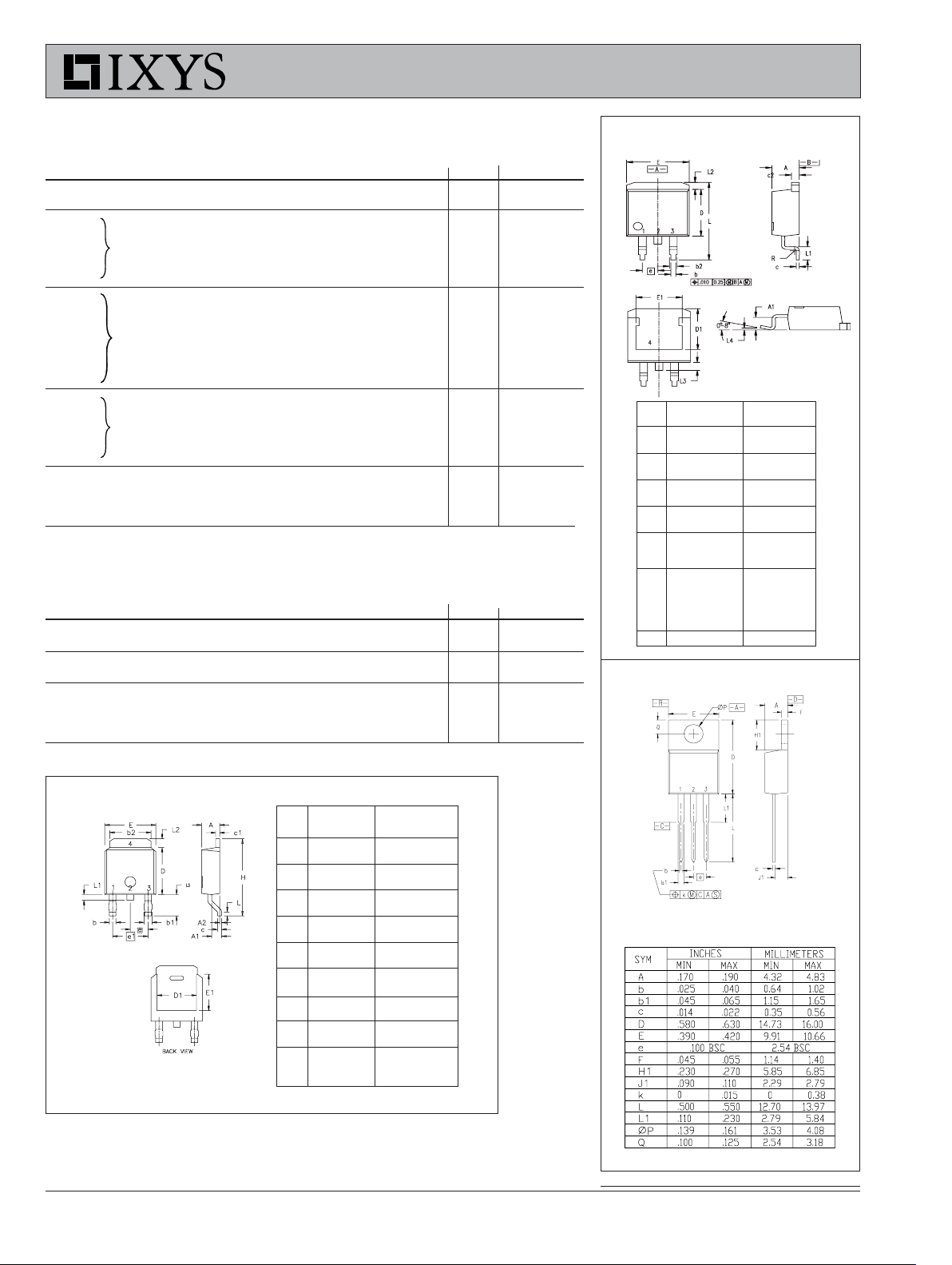
TO-263 (IXTA) Outline
Pins: 1 - Gate 2,4 - Drain
Dim. Millimeter Inches
Min. Max. Min. Max.
A 4.06 4.83 .160 .190
A1 2.03 2.79 .080 .110
b 0.51 0.99 .020 .039
b2 1.14 1.40 .045 .055
c 0.46 0.74 .018 .029
c2 1.14 1.40 .045 .055
D 8.64 9.65 .340 .380
D1 7.11 8.13 .280 .320
E 9.65 10.29 .380 .405
E1 6.86 8.13 .270 .320
e 2.54 BSC .100 BSC
L 14.61 15.88 .575 .625
L1 2.29 2.79 .090 .110
L2 1.02 1.40 .040 .055
L3 1.27 1.78 .050 .070
L4 0 0.38 0 .015
R 0.46 0.74 .018 .029
TO-220 (IXTP) Outline
3 - Source
TO-252 (IXTY) Outline
Dim. Millimeter Inches
Min. Max. Min. Max.
A 2.19 2.38 0.086 0.094
A1 0.89 1.14 0.035 0.045
A2 0 0.13 0 0.005
b 0.64 0.89 0.025 0.035
b1 0.76 1.14 0.030 0.045
b2 5.21 5.46 0.205 0.215
c 0.46 0.58 0.018 0.023
c1 0.46 0.58 0.018 0.023
D 5.97 6.22 0.235 0.245
D1 4.32 5.21 0.170 0.205
E 6.35 6.73 0.250 0.265
E1 4.32 5.21 0.170 0.205
e 2.28 BSC 0.090 BSC
e1 4.57 BSC 0.180 BSC
H 9.40 10.42 0.370 0.410
L 0.51 1.02 0.020 0.040
L1 0.64 1.02 0.025 0.040
Pins: 1 - Gate 2,4 - Drain
3 - Source
L2 0.89 1.27 0.035 0.050
L3 2.54 2.92 0.100 0.115
IXYS reserves the right to change limits, test conditions, and dimensions.
IXYS MOSFETs and IGBTs are covered by 4,835,592 4,931,844 5,049,961 5,237,481 6,162,665 6,404,065 B1 6,683,344 6,727,585
one or moreof the following U.S. patents: 4,850,072 5,017,508 5,063,307 5,381,025 6,259,123 B1 6,534,343 6,710,405B2 6,759,692
4,881,106 5,034,796 5,187,117 5,486,715 6,306,728 B1 6,583,505 6,710,463
Pins: 1 - Gate 2,4 - Drain
3 - Source

Fig. 1. Output Characteristics
º
C
@ 25
5
V
10V
GS
=
V
D S
7V
6V
5V
- Volts
4
3
- A mpe res
2
D
I
1
0
012345678
IXTA 5N50P IXTP 5N50P
IXTY 5N50P
Fig. 2. Extended Output Characteristics
º
C
@ 25
10
V
= 10V
GS
9
8
7
6
5
4
- Ampere s
D
I
3
2
1
0
0 3 6 9 12 15 18 21 24 27 30
7V
V
- Volts
D S
6V
5V
Fig. 3. Output Characteristics
º
@ 125
5
V
0.5 I
7V
V
D S
DS(on)
D25
4
3
- Amperes
2
D
I
1
0
024681012141618
Fig. 5. R
3.4
VGS = 10V
3
C
= 10V
GS
6V
5V
- Volts
Normalized to
Value vs. I
D
T
= 125ºC
J
Fig. 4. R
Normalized to 0.5 I
DS(on
)
Value vs. Junction Temperature
3.2
VGS = 10V
2.8
2.4
- Normalized
D S ( o n )
2
1.6
1.2
I
= 5A
D
I
= 2. 5 A
D
R
0.8
0.4
-50 -25 0 25 50 75 100 125 150
T
- Degrees Centigrade
J
Fig. 6. Drain Current vs. Case
Temper ature
6.0
5.0
D25
2.6
2.2
- Normalized
1.8
D S ( o n )
1.4
R
1
0.6
012345678910
© 2005 IXYS All rights reserved
I D - Amperes
T
J
= 25ºC
4.0
3.0
- Amperes
D
I
2.0
1.0
0.0
-50 -25 0 25 50 75 100 125 150
T
- Degrees Centigrade
C

IXTA 5N50P IXTP 5N50P
IXTY 5N50P
Fig. 7. Input Admittance
7
6
5
4
3
- A mpe res
D
I
2
1
0
4 4.5 5 5.5 6 6.5 7
TJ = 125ºC
25
-40
º
º
V
G S
C
C
- Volts
Fig. 9. Source Current vs.
Source-To-Drain Voltage
15
12
9
- Amperes
6
S
I
3
0
0.4 0.5 0.6 0.7 0.8 0.9 1
T
= 125ºC
J
V
S D
- Volts
T
J
= 25ºC
Fig. 8. Transconductance
9
8
TJ = -40ºC
7
6
5
- Siemens
4
f s
3
g
2
1
0
01234567
25
125
º
C
º
C
I
- Amperes
D
Fig. 10. Gate Charge
10
9
V
= 250V
DS
8
7
6
5
- V ol t s
G S
4
V
3
2
1
0
= 2. 5A
I
D
I
= 10m A
G
02468101214
Q G - nanoCoulombs
Fig. 11. Capacitance
10000
f = 1MHz
1000
100
10
C
C
C
Capacitance - picoFarads
1
0 5 10 15 20 25 30 35 40
V
- Volts
D S
iss
oss
rss
100
R
DS(on)
10
- Amperes
D
I
1
0.1
10 100 1000
Fig. 12. Forward-Bias
Safe Operat ing Area
Limit
DC
V
- Volts
D S
IXYS reserves the right to change limits, test conditions, and dimensions.
IXYS MOSFETs and IGBTs are covered by 4,835,592 4,931,844 5,049,961 5,237,481 6,162,665 6,404,065 B1 6,683,344 6,727,585
one or moreof the following U.S. patents: 4,850,072 5,017,508 5,063,307 5,381,025 6,259,123 B1 6,534,343 6,710,405B2 6,759,692
4,881,106 5,034,796 5,187,117 5,486,715 6,306,728 B1 6,583,505 6,710,463
TJ = 150ºC
= 25ºC
T
C
25µs
100 µ s
1m s
10 m s

IXTA 5N50P IXTP 5N50P
IXTY 5N50P
Fig. 13. Maximum Transient Thermal Resistance
10.00
1.00
ºC / W
-
( t h ) J C
0.10
R
0.01
0.00001 0.0001 0.001 0.01 0.1 1 10
Pulse Width - Seconds
© 2005 IXYS All rights reserved
 Loading...