IXYS IXSX35N120AU1 Datasheet

High Voltage IXSX 35N120AU1
IGBT with Diode
Combi Pack
Short Circuit SOA Capability
V
CES
I
C25
V
CE(SAT)
= 1200 V
= 70 A
= 4 V
Symbol Test Conditions Maximum Ratings
V
CES
V
CGR
V
GES
V
GEM
I
C25
I
C90
I
CM
SSOA V
(RBSOA) Clamped inductive load, L = 30 mH @ 0.8 V
t
SC
(SCSOA) RG = 22 W, non repetitive
P
C
T
J
T
JM
T
stg
T
L
TJ= 25°C to 150°C 1200 V
TJ= 25°C to 150°C; RGE = 1 MW 1200 V
Continuous ±20 V
Transient ±30 V
TC= 25°C70A
TC= 90°C35A
TC= 25°C, 1 ms 140 A
= 15 V, TJ = 125°C, RG = 22 W ICM = 70 A
GE
CES
VGE= 15 V, VCE = 720 V, TJ = 125°C 10ms
TC= 25°C IGBT 300 W
Diode 190 W
-55 ... +150 °C
150 °C
-55 ... +150 °C
1.6 mm (0.063 in) from case for 10 s 300 °C
Weight TO-247 HL 6 g
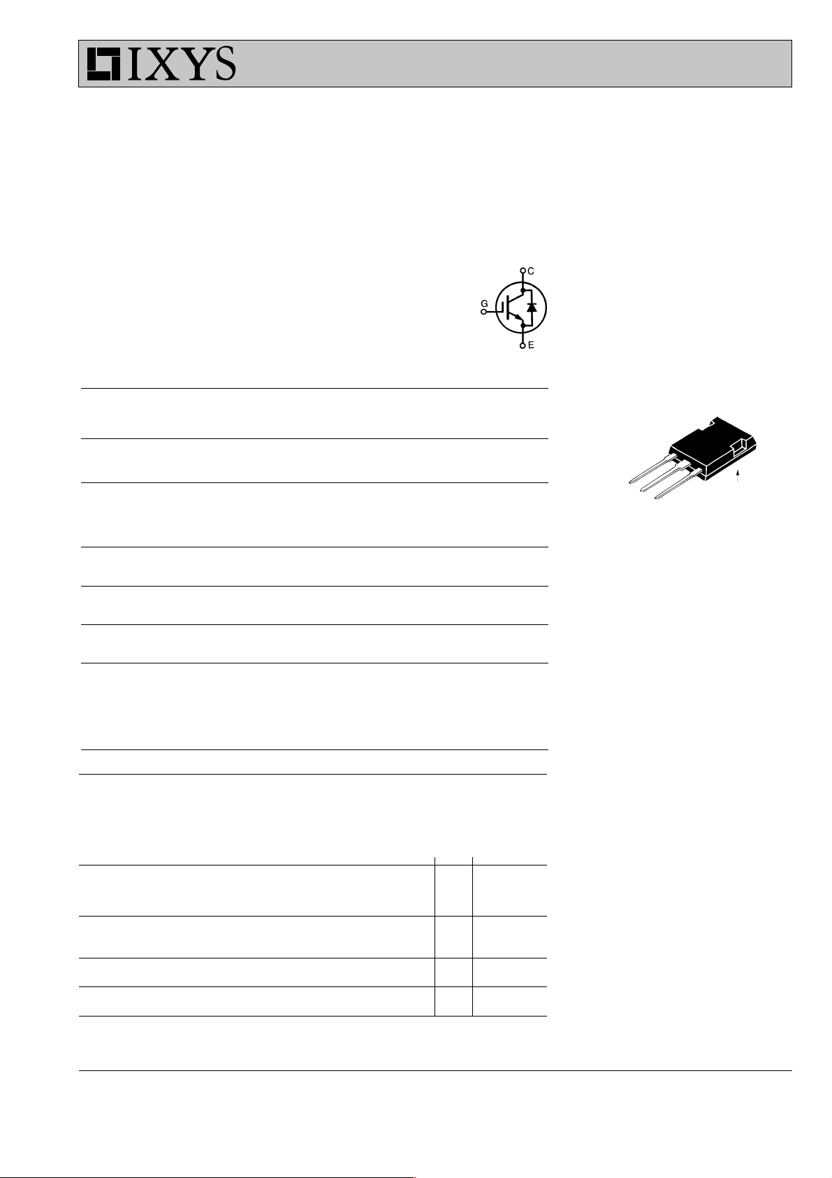
PLUS TO-247
TM
(IXSX35N120AU1)
G
C
E
G = Gate, C = Collector,
E = Emitter, TAB = Collector
C (TAB)
Features
• Hole-less TO-247 package for clip
mounting
• High frequency IGBT and anti-parallel
FRED in one package
• Low V
CE(sat)
- for minimum on-state conduction
losses
• MOS Gate turn-on
- drive simplicity
• Fast Recovery Epitaxial Diode (FRED)
- soft recovery with low I
RM
Symbol Test Conditions Characteristic Values
(TJ = 25°C, unless otherwise specified)
min. typ. max.
BV
CES
V
GE(th)
I
VCE= 0.8 • V
CES
I
GES
V
CE(sat)
IXYS reserves the right to change limits, test conditions, and dimensions.
IC= 5 mA, VGE = 0 V 1200 V
IC= 4 mA, VCE = V
VGE= 0 V TJ = 125°C15mA
CES
GE
TJ = 25°C 750 mA
48V
VCE= 0 V, VGE = ±20 V ±100 nA
IC= I
, VGE = 15 V 4 V
C90
© 2000 IXYS All rights reserved
Applications
• AC motor speed control
• DC servo and robot drives
• DC choppers
• Uninterruptible power supplies (UPS)
• Switch-mode and resonant-mode
power supplies
Advantages
• Space savings (two devices in one
package)
• Reduces assembly time and cost
• High power density
97514D (7/00)
1 - 5

IXSX 35N120AU1
Symbol Test Conditions Characteristic Values
(TJ = 25°C, unless otherwise specified)
min. typ. max.
g
fs
IC= I
; VCE = 10 V, 20 26 S
C90
Pulse test, t £ 300 ms, duty cycle £ 2 %
I
C
C
C
Q
Q
Q
t
t
t
t
E
t
t
E
t
t
E
C(on)
ies
oes
res
g
ge
gc
d(on)
ri
d(off)
fi
off
d(on)
ri
on
d(off)
fi
off
VGE = 15 V, VCE = 10 V 170 A
3900 pF
VCE = 25 V, VGE = 0 V, f = 1 MHz 295 pF
60 pF
150 190 nC
IC = I
, VGE = 15 V, VCE = 0.5 V
C90
CES
40 60 nC
70 100 nC
Inductive load, TJ = 25°C
I
= I
, VGE = 15 V,
C
C90
L = 100 mH, VCE = 0.8 V
Switching times may increase for V
(Clamp) > 0.8 • V
increased R
CES
G
, RG = 2.7 W
CES
, higher TJ or
Inductive load, TJ = 125°C
I
= I
, VGE = 15 V,
C
C90
L = 100 mH, VCE = 0.8 V
Switching times may increase for V
(Clamp) > 0.8 • V
increased R
CES
G
, RG = 2.7 W
CES
, higher TJ or
CE
CE
80 ns
150 ns
400 900 ns
500 700 ns
10 mJ
80 ns
150 ns
8mJ
400 ns
700 ns
15 mJ
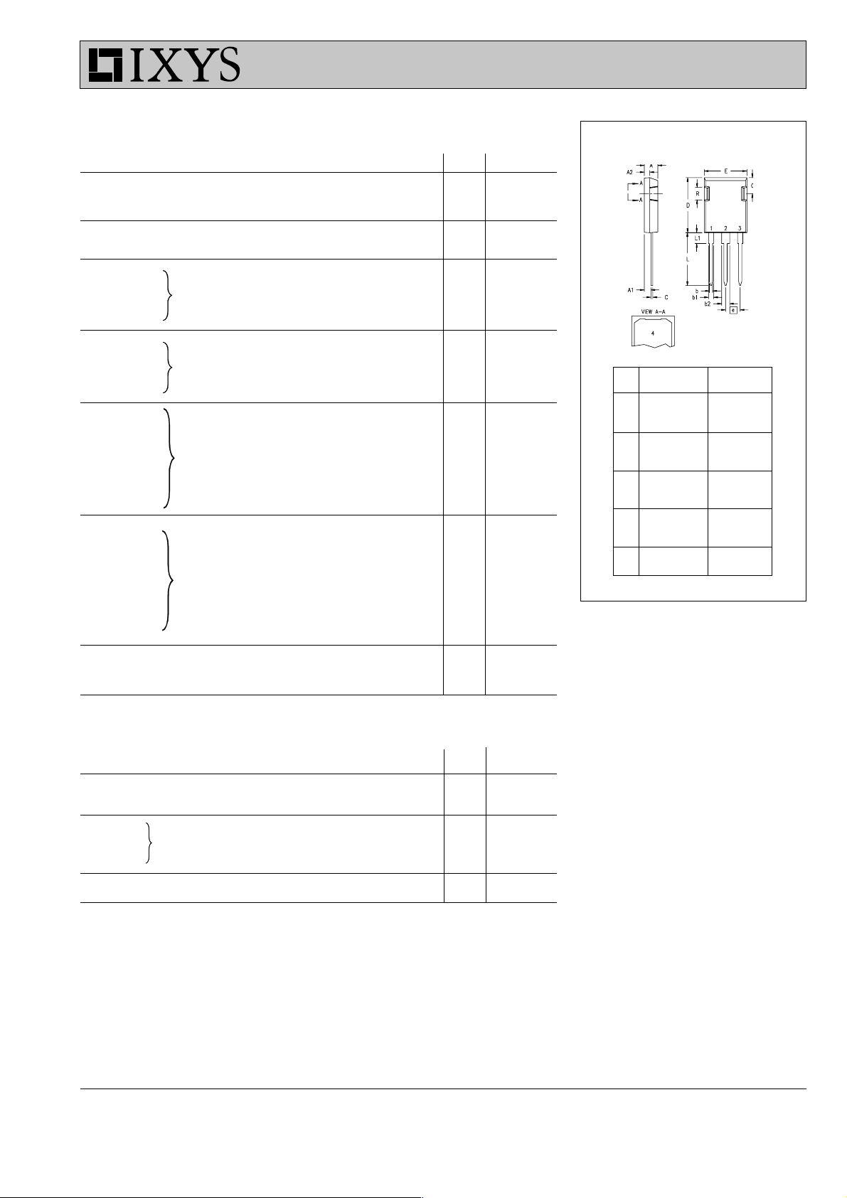
PLUS247TM (IXSX)
Dim. Millimeter Inches
Min. Max. Min. Max.
A 4.83 5.21 .190 .205
2.29 2.54 .090 .100
A
1
A21.91 2.16 .075 .085
b 1.14 1.40 .045 .055
b
1.91 2.13 .075 .084
1
b22.92 3.12 .115 .123
C 0.61 0.80 .024 .031
D 20.80 21.34 .819 .840
E 15.75 16.13 .620 .635
e 5.45 BSC .215 BSC
L 19.81 20.32 .780 .800
L1 3.81 4.32 .150 .170
Q 5.59 6.20 .220 .244
R 4.32 4.83 .170 .190
R
thJC
R
thCK
0.15 K/W
0.42 K/W
Reverse Diode (FRED) Characteristic Values
(TJ = 25°C, unless otherwise specified)
Symbol Test Conditions min. typ. max.
V
F
I
RM
t
rr
R
thJC
IF = I
, VGE = 0 V, Pulse test, 2.35 V
C90
t £ 300 ms, duty cycle d £ 2 %, TJ = 125°C
IF = I
, VGE = 0 V, -diF/dt = 480 A/ms3236A
C90
VR = 540 V TJ = 100°C 225 ns
IF = 1 A; -di/dt = 200 A/ms; VR = 30 V TJ =25°C4060ns
0.65 K/W
© 2000 IXYS All rights reserved
IXYS MOSFETS and IGBTs are covered by one or more of the following U.S. patents:
4,835,592 4,881,106 5,017,508 5,049,961 5,187,117 5,486,715
4,850,072 4,931,844 5,034,796 5,063,307 5,237,481 5,381,025
2 - 5
 Loading...