IXYS IXSA15N120B, IXSP15N120B Datasheet

Advance Technical Information
HIGH Voltage IGBT
IXSA 15N120B
IXSP 15N120B
"S" Series - Improved SCSOA Capability
Symbol Test Conditions Maximum Ratings
V
CES
V
CGR
V
GES
V
GEM
I
C25
I
C90
I
CM
SSOA V
(RBSOA) Clamped inductive load @ 0.8 V
t
SC
P
C
T
J
T
JM
T
stg
M
d
Maximum lead temperature for soldering 300 °C
1.6 mm (0.062 in.) from case for 10 s
Maximum tab temperature for soldering (TO-263) 260 °C
Weight TO-220 4 g
T
= 25°C to 150°C 1200 V
J
T
= 25°C to 150°C; RGE = 1 MΩ 1200 V
J
Continuous ±20 V
Transient ±30 V
T
= 25°C30A
C
T
= 90°C15A
C
T
= 25°C, 1 ms 60 A
C
= 15 V, T
GE
T
= 125°C, V
J
Non repetitive
T
= 25°C 150 W
C
= 125°C, RG = 10 Ω I
J
= 720 V; VGE = 15 V, R
GE
= 10 Ω 10 µs
G
= 40 A
CM
CES
-55 ... +150 °C
150 °C
-55 ... +150 °C
Mounting torque (TO-247) 1.13/10 Nm/lb.in.
TO-263 2 g
V
CES
I
C25
V
CE(sat)
=1200 V
= 30 A
= 3.4 V
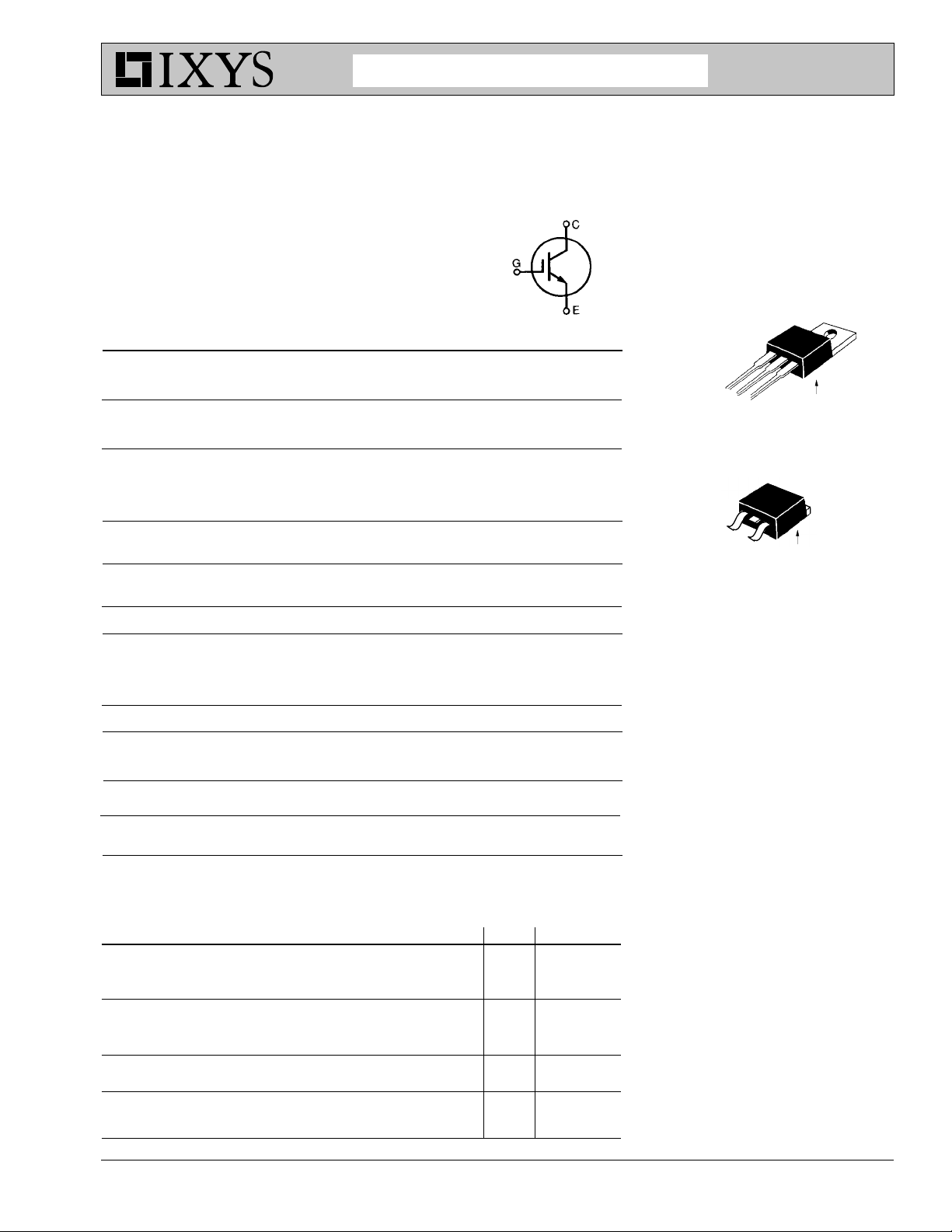
TO-220AB (IXSP)
G
C
E
C (TAB)
TO-263 AA (IXSA)
G
E
C (TAB)
Features
•International standard packages
JEDEC TO-220AB and TO-263AA
•Low switching losses, low V
(sat)
•MOS Gate turn-on
- drive simplicity
Symbol Test Conditions Characteristic Values
(TJ = 25°C, unless otherwise specified) Min. Typ. Max.
BV
V
I
CES
I
GES
V
CES
GE(th)
CE(sat)
IC= 250 µA, VGE = 0 V 1200 V
IC= 250 µA, VCE = V
VCE = V
CES
= 0 V TJ = 125°C 2.5 mA
V
GE
GE
TJ = 25°C50µA
36V
VCE= 0 V, VGE = ±20 V ±100 nA
IC= I
, VGE = 15 3.0 3.4 V
CE90
TJ = 125°C 2.8 V
© 2002 IXYS All rights reserved
Applications
•AC motor speed control
•DC servo and robot drives
•DC choppers
•Uninterruptible power supplies (UPS)
•Switch-mode and resonant-mode
power supplies
Advantages
•Easy to mount with one screw
•Reduces assembly time and cost
•High power density
98922 (5/02)

IXSA 15N120B
IXSP 15N120B
Symbol Test Conditions Characteristic Values
(TJ = 25°C, unless otherwise specified) Min. Typ. Max.
g
fs
IC= I
; VCE = 10 V, 7 9.5 S
C90
Note2
C
C
C
Q
Q
Q
t
t
t
t
E
t
t
E
t
t
E
ies
oes
res
g
ge
gc
d(on)
ri
d(off)
fi
off
d(on)
ri
on
d(off)
fi
off
VCE = 25 V, VGE = 0 V, f = 1 MHz 98 pF
IC= I
Inductive load, TJ = 25
I
C
VCE= 960 V, RG = R
, VGE = 15 V, VCE = 0.5 V
C90
= I
, VGE = 15 V
C90
= 10 Ω
off
°°
°C
°°
CES
Note3
= 10 Ω
off
°°
°C
°°
Inductive load, TJ = 125
IC= I
, VGE = 15 V
C90
VCE= 960 V, RG = R
Note3
1400 pF
37 pF
57 nC
14 nC
25 nC
30 ns
25 ns
148 280 ns
160 320 ns
1.75 3.0 mJ
30 ns
25 ns
1.1 mJ
265 ns
298 ns
3.1 mJ
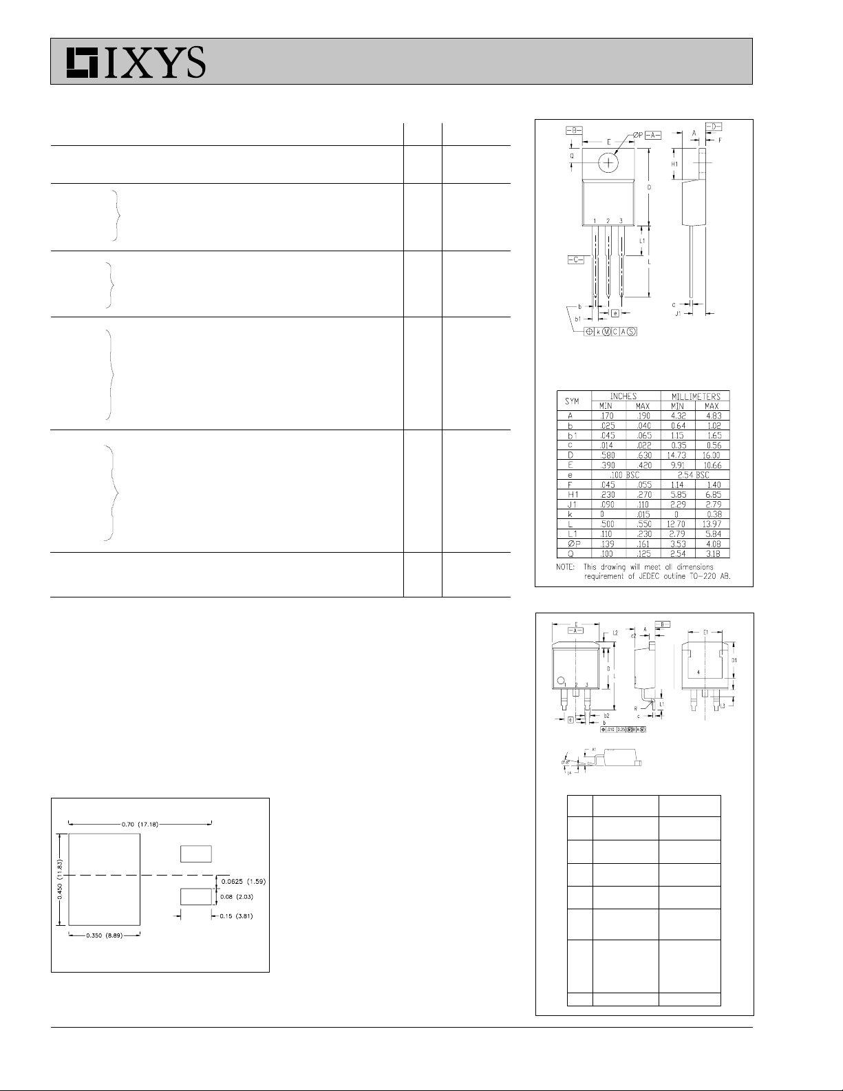
TO-220 AB Dimensions
Pins: 1 - Gate 2 - Collector
3 - Emitter 4 - Collector
Bottom Side
R
thJC
R
thCK
TO-220 0.5 K/W
0.83 K/W
TO-263 AA Outline
Notes: 1. Device must be heatsunk for high temperature leakage current
measurements to avoid thermal runaway.
2. Pulse test, t ≤ 300 µs, duty cycle ≤ 2 %
3. Switching times may increase for VCE (Clamp) > 0.8 V
increased RG.
Min. Recommended Footprint
(Dimensions in inches and mm)
IXYS reserves the right to change limits, test conditions, and dimensions.
IXYS MOSFETs and IGBTs are covered by one or more of the following U.S. patents: 4,835,592 4,881,106 5,017,508 5,049,961 5,187,117 5,486,715 6,306,728B1
, higher TJ or
CES
1. Gate
2. Collector
3. Emitter
4. Collector
Dim. Millimeter Inches
Min. Max. Min. Max.
A 4.06 4.83 .160 .190
A1 2.03 2.79 .080 .110
b 0.51 0.99 .020 .039
b2 1.14 1.40 .045 .055
c 0.46 0.74 .018 .029
c2 1.14 1.40 .045 .055
D 8.64 9.65 .340 .380
D1 7.11 8.13 .280 .320
E 9.65 10.29 .380 .405
E1 6.86 8.13 .270 .320
e 2.54 B SC .100 B SC
L 14.61 15.88 .575 .625
L1 2.29 2.79 .090 .110
L2 1.02 1.40 .040 .055
L3 1.27 1.78 .050 .070
L4 0 0.38 0 .015
R 0.46 0.74 .018 .029
4,850,072 4,931,844 5,034,796 5,063,307 5,237,481 5,381,025
Bottom Side
 Loading...