I - 35
© 1998 IXYS All rights reserved
High Performance Dual PWM Microstepping Controller
Type Package Temperature Range
IXMS150 PSI 24-Pin Skinny DIP -40°C to +85°C
The IXMS150 is a high performance
monolithic 2-channel PWM controller.
Implemented in CMOS, the low power
IXMS150 precisely controls the current
in each of two separate power H-bridge
drivers using unique sampling and
signal processing techniques. Each
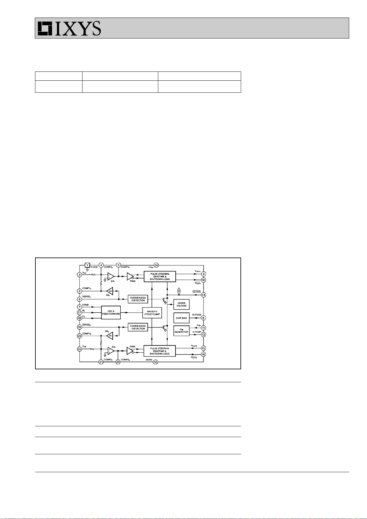
channel contains an error amplifier,
PWM, feedback amplifier, and protection circuitry. Protection features include
over/excess current shutdown, min/max
duty cycle clamp, under voltage lockout, dead time insertion, and a shutdown
input for over-temp or other external
fault circuitry. Other features include a
common oscillator, feedforward circuit
for motor supply compensation, and an
onchip negative bias generator.
The IXMS150 has been optimized for
microstep control of two phase step
motors. Due to its high level of accu-
racy, the IXMS150 will allow a designer
to implement a control system with a
resolution in excess of 250 microsteps
per step, or 50,000 steps per revolution
with a 200 step per revolution step
motor. The IXMS150 greatly improves
positioning accuracy and virtually
eliminates low speed velocity ripple and
resonance effects at a fraction of the cost
of a board level microstepping system.
Other applications which the IXMS150
is designed for include control of two
single-phase (DC) motors or control of
synchronous reluctance motors. The
IXMS150 is ideal for robotics, printers,
plotters, and x-y tables and can facilitate the construction of very sophisticated
positioning control systems while significantly reducing
component cost, board
space, design time and systems cost.
Features
l Two complete, synchronous PWMs
l Command input range ±2.0 V full
scale
l ±0.625 V full scale current feedback
signal
l 1% gain matching between channels
without external trim
l 1.6% gain linearity
l Feedforward to compensate for
motor supply variations
l Only one sense resistor per H-bridge
needed
l Onboard two level current limiting
l Undervoltage lockout assures proper
behavior on power up and power
down
l Enable input for external over
temperature or fault circuit input
l Duty cycles limited for AC coupled
gate drive
l Wide range of built in dead time.
l On board negative power supply
generator
l Single +12 V supply operation
l 24-pin DIP package
Applications
l Full, half quarter, or microstepping
2-phase step motor position
controller
l Dual DC servo motor torque
controller
l Solenoid actuator force controller
l General 2-channel current-
commanded PWM control
Block diagram of IXMS 150
Symbol Definition Max. Ratings
V
DD
Supply voltage -0.3...15 V
Operating range 10.8...13.2 V
Common-mode-range -15...15 V
Differential Input voltage ¬ ±30 V
V
IN
Input voltage ¬ -15...15 V
V
O
Output voltage -0.3...VDD+0.3 V
P
D
Maximum power dissipation 500 mW
T
A
Ambient temperature range -40...85 °C
T
stg
Storage temperature range -55...125 °C
¬ Input voltage may not exceed either supply rail by more than 0.3 V at any time.
IXYS reserves the right to change limits, test conditions and dimensions.

I - 36
© 1998 IXYS All rights reserved
IXMS 150
Symbol Definition/Condition Characteristic Values
(VDD = 12 V, T
A
= 25°C unless otherwise specified)
min. typ. max.
Oscillator
f
OSC
Frequency C
o
10 400 kHz
V
A(p-p)
Amplitude FFWD = OPEN 7 V
Z
OUT
Output Impedance ± I
OUT
= 400 µA 2.5 mΩ
Resistance Range R
o
15 100 kΩ
Capacitance Range C
o
100 2000 pF
Feed Forward
V
FFWD
Feedforward FFWD = Open 3.5 V
Voltage
Z
INFF
Impedance to AGND 25 45 kΩ
Analog Inputs
V
FS
Input FullScale V
INA
DC ±2V
V
INB
Z
IN1
VIN to Comp
2
DC 20 32 kΩ
Impedance
Z
IN2
Comp1 to Comp
2
DC 12 20 kΩ
Impedance
Sense Inputs SENSE
A
V
SENSE
Full Scale Input SENSE
B
DC ±0.625 V
Z
INS
Input Impedance DC 100 200 kΩ
Protection Circuit SENSE
A
V
OV-1
Over Current SENSE
B
0.8 0.95 1.0 V
Voltage
t
OV-1
Reset Pulse Width 0.5 1 µs
V
EX-1
Excess Current Voltage 3.45 3.6 3.75 V
t
EX-1
Reset Pulse Width 300 ns
Under Voltage
V
UV
Minimum V
DD
OUTDIS 7.5 8 8.5 V
I
IH
Input High Current V
IH
= 11.5 V 100 µA
I
IL
Input Low Current V
IL
= 0.5 V 1.8 mA
Outputs
V
OH
Output High V
OUTA
, V
OUTA
IOH = -10 mA 8.0 11.2 V
Voltage
V
OL
Output Low V
OUTB
, V
OUTB
I
OL
= 10 mA 0.8 1.1 V
Voltage
t
r
Rise Time CL = 100 pF 35 50 ns
t
f
Fall Time CL = 100 pF 35 50 ns
T
DT
Dead-Time Co = 180 pF 200 300 450 ns
T
MIN
Minimum Pulse Width C
p
= 30 pF 0.6 0.8 1.5 µs
VBB Generator
V
BBmin
Minimum V
BB
OUTDIS -1.4 -1.9 V
Negative Bias = V
DD
V
BB
Negative Bias I
OUT
= -3 mA -2.1 -2.4 V
Voltage
V
REG
Load Regulation f
OSC
60 mV
= 100 kHz
V
OH
Output High Volt. C
PUMP
IOH = -10 mA 11.2 V
V
OL
Output Low Volt. IOL = 32 mA 0.8 V
Supply
I
DD1
Idle Current V
DD
VIN = 0 16 26 mA
I
DD2
Operating Current f
OSC
15 45 mA
= 100 kHz
V
BYPASS
Bypass Voltage BYPASS 5.9 16.1 V
Z
INBP
Impedance to AGND 9 16 kΩ
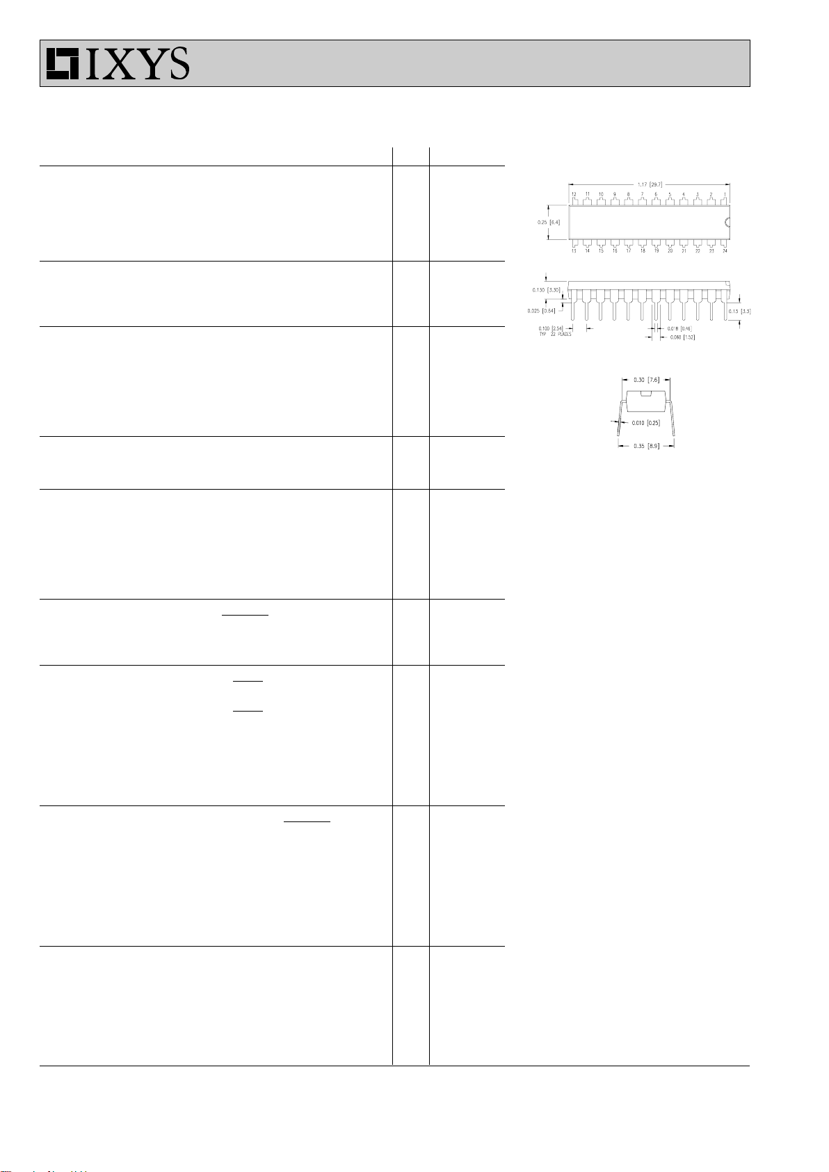
Dimensions in inch (1" = 25.4 mm)
24-Pin Skinny DIP

I - 37
© 1998 IXYS All rights reserved
IXMS 150
Pin Description IXMS 150
Nomenclature of Dual PWM
Microstepping Controller
Sym. Pin Description
AGND 1 Analog Ground
COMP 2 Analog Compensation
4 (see application notes for
5 recommendations).
20
21
23
VIN 3 Analog Input: The analog
22 input range is ± 2 V. A low
output im pedance voltage
source should drive these
pins. The input is greater
than 20 kΩ.
SENSE 6 Analog Sense: Each of the
19 phases sense resistors are
connected to these pins.
Input range is +0.625 V.
FFWD 7 FFWD, for Motor High
Voltage Compensation: A
voltage on this pin sets the
oscillator amplitude. Input
range = 0.9-4 V (see
application notes for
recommendations).
BY- 8 Filter Cap: A capacitor on
PASS this pin provides filtering to
the internal bias network.
VOUT 9 Output Stage: To drive
10 buffered power MOSFET
15 H-Bridge.
16
VBB 11 Negative Bias Generator
Output: For internal use by
the IXMS 150.
DGND 12 Digital Ground
CPUMP 13 Charge Pump Capacitor:
Used by the internal
Negative Bias Generator.
OUTDIS 14 Digital ENABLE input and
STATUS output: Forcing this
pin low causes pins 9, 10,
15, and 16 to go low, disabling the H-bridge. When uses
as an output, a low state on
this pin indicates an over
current, excess current, or
insufficient +VDD or VBB error
condition.
RO, CO17 Oscillator Frequency and
18 Dead-time set: Independent
adjustment can be made to
the oscillator frequency and
dead-time (see applications
notes).
VDD 24 Positive Supply Voltage
* Pin numbers in parantheses are
associated with channel B.
IXMS 150 PS I (Example)
IX IXYS
MS 150 Dual PWM Controller
Package Type
PS Plastic Skinny DIP
Temperature Range
I Industrial
 Loading...