IXYS IXHQ100SI, IXHQ100PI Datasheet

1:0321
1:03 51
Negative Voltage Hot Swap Controller
with Active Power Filter
Features
Live Insertion and Removal Power Manager
Adjustable Power-on slew rate
Autodetect of Load Open Circuit or -VIN
Disconnection
Controlled Time-Delay
Operates from 9 V to External MOSFET Voltage
Limit
Fault Indication Output (microprocessor reset).
Board Insertion/Removal Detector Input
Protection During Turn-On
Low frequency Power Active Filter
Adjustable Electronic Circuit Breaker
Vin undervoltage with GSNSin input
Applications
Arcless card insertion and removal
Central Office Switching Hardware
Circuit Boards From -48 V Distributed Power
Supplies
Circuit Board Power Manager and Noise Filter
Circuit Board Hot Swap Protector and Manager
Electronic Circuit Breaker
Wireless Local Loop Antennas
Cable TV Antenna
Description
The IXHQ100 is a live insertion and removal hot swap
controller with a built-in power noise filter. It incorporates all the active circuitry necessary to protect circuit
boards during live insertion or removal (insertion or
removal when the system power is active). Additionally,
the IXHQ100 incorporates two unique features: power
active filter for powerline noise suppression and power
auto-disconnect detector which eliminates the need of
additional staggered pins.
The IXHQ100 shunt regulator ensures a wide operating
voltage range (with the external MOSFET breakdown
voltage as limit). The active power filter reduces power
source output impedance, producing "clean" load
power. The IXHQ100 allows continuous load current
rise adjustments, presettable maximum current limits,
and user selectable fault indication turn off times for
resetting µPs and other synchronous board level sys-
tems. For added flexibility, GSNSin pin is available to
implement either circuit board insertion/removal detection or ground detection.
US Patents Pending.
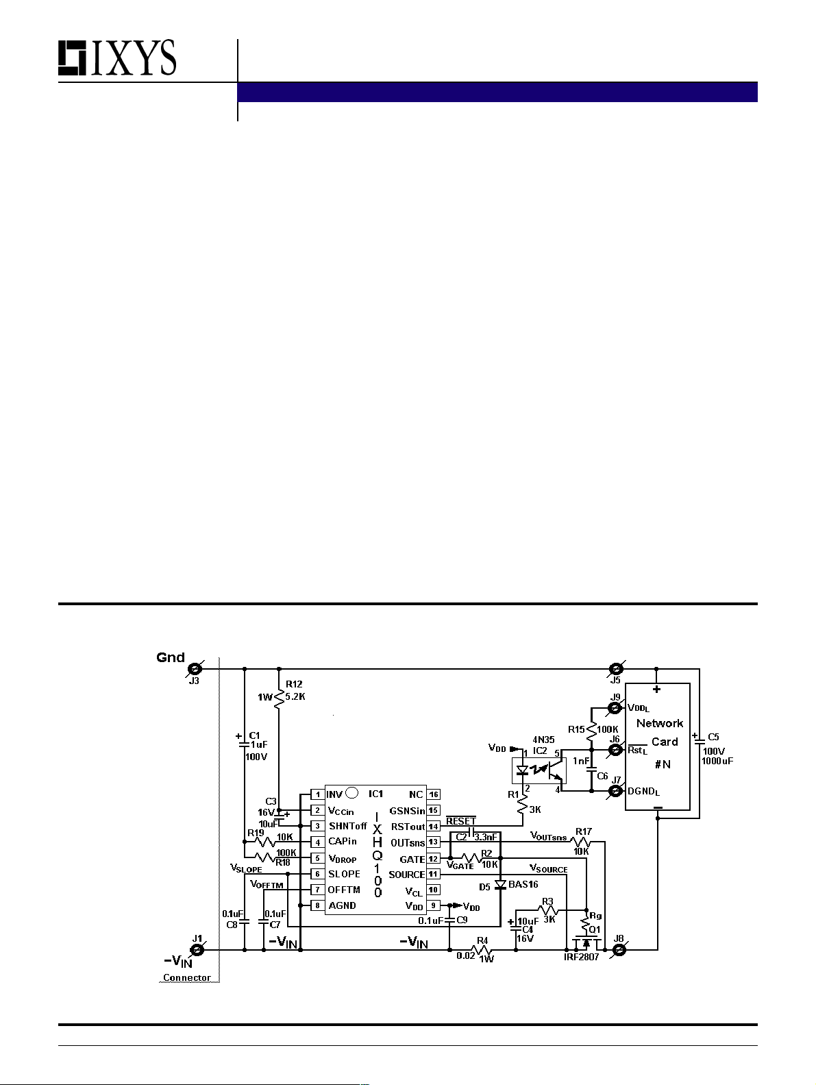
Typical Application with Auto-Disconnect Detector
CAUTION: These devices are
sensitvie to electrostatic discharge;
take caution when handling and
assembling this component.
Figure 1Figure 1
Figure 1
Figure 1Figure 1
IXYS reserves the right to change limits, test conditions and dimensions.
Copyright © IXYS CORPORATION 2000
www.ixys.com 98716 (08/14/00)
1

Absolute Maximum RatingsAbsolute Maximum Ratings
Absolute Maximum Ratings
Absolute Maximum RatingsAbsolute Maximum Ratings
Symbol Symbol
Symbol
Symbol Symbol
Definition Definition
Definition
Definition Definition
Max. Rating Max. Rating
Max. Rating
Max. Rating Max. Rating
Pin DescriptionPin Description
Pin Description
Pin DescriptionPin Description
IXHQ 100PI
IXHQ 100SI
VCC-V
AGND
Voltage applied V
to AGND Shunt Off: -0.3 V to 16 V
CCin
Shunt On: -0.3 V to 14 V
Shunt On for 10 seconds 14V to 16 V
All other pins except V
I
VDD
T
JM
T
J0
T
stg
I
DD
Electrical CharacteristicsElectrical Characteristics
Electrical Characteristics
Electrical CharacteristicsElectrical Characteristics
Unless otherwise noted, TA = 25 oC; -VIN= 48 V, AGND connected to -VIN, V
with respect to AGND. IXHQ100 configured as described in
SymbolSymbol
Symbol
SymbolSymbol
I
CC
VDD Load Current 60 mA
Maximum Junction Temperature 125 oC
Operating Temperature Range -40 oC to 85 oC
Storage Temperature Range -40 oC to 150 oC
Supply Current with Shunt On 25 mA
Parameter Parameter
Parameter
Parameter Parameter
Supply current VCC=12 V, V
DC
-0.3 V to V
Test Conditions
Test ConditionsTest Conditions
Test Conditions
Test ConditionsTest Conditions
SHUNToff
all outputs unloaded.
V
CCSHUNT
V
shunt regulation ICC forced to 10 mA 12 13.8 16 V
CC
voltage when shunt is off
V
THSHUNToff
SHUNToff input VCC = 15 V, monitor RST
threshold voltage
I
SHUNToff
SHUNToff input -1 0 1 µA
bias current
V
THINV
INV input VCC = 12 V, monitor RST
threshold voltage
R
INV
INV input 70 130 180 KΩ
resistance
V
THGSNS
GSNS sense input VCC = 12 V, monitor RST
threshold voltage
I
GSNSin
GSNSin input -2.6 -2.3 -2 µA
bias current
I
CAPin
V
R
VDROP
VDROP
CAPin input bias current -1 0 1 µA
Active filter offset voltage 0.7 0.9 1.1 V
V
input resistance 50 70 90 KΩ
DROP
+ 0.3 V
CCin
SHUNToff
.
= 5 V, V
= 12 V, V
CC
= 12 V. All voltage measurements
GSNSin
MinMin
Min
MinMin
TypTyp
Typ
TypTyp
MaxMax
Max
MaxMax
Units Units
Units
Units Units
= VCC,23mA
OUT
OUT
OUT
1 1.5 2 V
6810V
4.5 5.8 6 V
I
SLOPE
R
SLOPEDCHG
I
OFFTM
R
OFFTMCHG
V
THOFFTM
V
CL
SLOPE capacitor V
charging current V
SLOPE capacitor V
discharge resistance V
OFFTM capacitor V
charging current V
= 5 V, V
OFFTM
= 5 V
CAPin
= 5 V, IVT = V
DROP
= 0 V, V
SOURCE
= 5 V, V
DROP
= 5 V
CAPin
= 0 V 70 85 110 mA
GSOURCE
CC
= 5 V
CAPin
= 0 V 80 100 120 mA
SOURCE
90 200 Ω
OFFTM capacitor 111 200 Ω
discharge resistance
OFFTM input threshold OFFTM input voltage when SLOPE 3.8 4.5 5.5 V
voltage input voltage starts its ramp
Overcurrent threshold bias voltage 90 125 150 mV
2

Electrical Characteristics Electrical Characteristics
Electrical Characteristics (continued)
Electrical Characteristics Electrical Characteristics
SymbolSymbol
Symbol
SymbolSymbol
Parameter Parameter
Parameter
Parameter Parameter
Test ConditionsTest Conditions
Test Conditions
Test ConditionsTest Conditions
MinMin
Min
MinMin
IXHQ 100PI
IXHQ 100SI
TypTyp
Typ
TypTyp
MaxMax
Max
MaxMax
Units Units
Units
Units Units
R
VCL
t
OC
VCL bias resistance 4 6 10 kΩ
Overcurrent detection V
to GATE output delay V
= 0 V; V
CAPin
input is a step at t = 0s
SOURCE
OUTsns
= 5 V 20 30 ms
from 0 V to 200 mV
dv
/dt GATE output slew rate C
GATE
V
GATE
Maximum GATE V
output voltage V
I
GATE
I
GATE
GATE pull-up current Gate drive on, V
GATE pull-down Gate drive off 10 20 mA
current V
V
DD
VDD regulator output 3.3K Resistive load 5 5.75 6.5 V
= 100 nF 0.5 0.8 1.1 V/ms
SLOPE
CAPin
OUTsns
GATE
= 0 V; R
= 5 V
= 10 V
= 10 KΩ 13.8 15 V
load
= 0 V -15 -10 mA
GATE
Voltage between VDD output and AGND
I
RSTout
t
RST
V
ad
RSTout drive current Force V
=1 V during fault condition 2.4 3 3.6 mA
RSTout
RST pulse width 200 500 1000 ns
Auto-Detect threshold Gate drive on; ramp V
; monitor -10 12 20 mV
OUTsns
RST until it pulses.
Note 1: Operating the device beyond parameters with listed “absolute maximum ratings” may cause permanent damage to the
device. Typical values indicate conditions for which the device is intended to be functional, but do not guarantee specific
performance limits. The guaranteed specifications apply only for the test conditions listed. Exposure to absolute maximum
rated conditions for extended periods may affect device reliability.
Note2: All voltages are relative to ground unless otherwise specified.
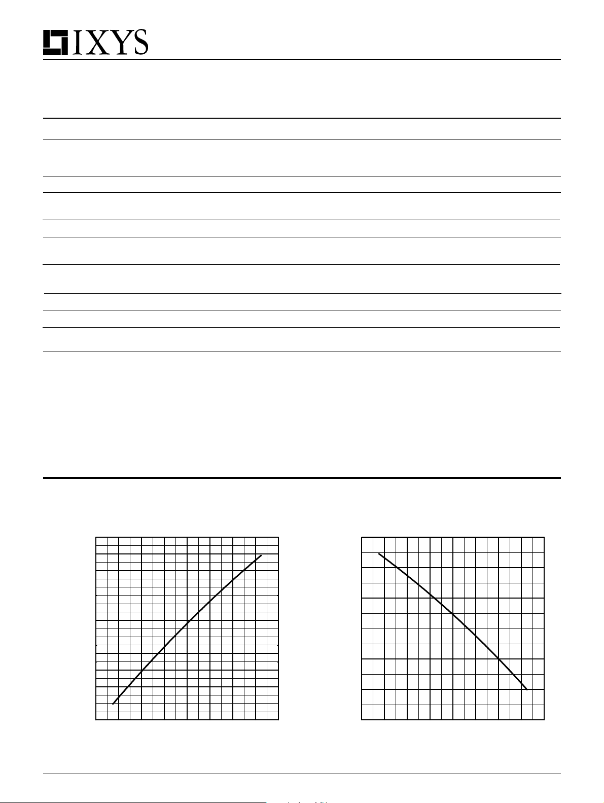
Typical Performance CharacteristicsTypical Performance Characteristics
Typical Performance Characteristics
Typical Performance CharacteristicsTypical Performance Characteristics
Graph 1: Icc vs. TemperatureGraph 1: Icc vs. Temperature
Graph 1: Icc vs. Temperature
Graph 1: Icc vs. TemperatureGraph 1: Icc vs. Temperature
2.18
2.16
2.14
2.12
2.10
2.08
2.06
Icc (mA)
2.04
2.02
2.00
1.98
1.96
-60 -40 -20 0 20 40 60 80 100
Temperature (oC)
Graph 2: Regulator Output Voltage vs. TemperatureGraph 2: Regulator Output Voltage vs. Temperature
Graph 2: Regulator Output Voltage vs. Temperature
Graph 2: Regulator Output Voltage vs. TemperatureGraph 2: Regulator Output Voltage vs. Temperature
6.0
5.9
5.8
5.7
5.6
5.5
Regulator Output Voltage (V)
5.4
-60 -40 -20 0 20 40 60 80 100
Temperature (oC)
3
 Loading...