

查询IXGH39N60B供应商
HiPerFAST
TM
IGBT IXGH39N60B V
IXGH39N60BD1 I
IXGT39N60B V
IXGT39N60BD1 t
Preliminary data
(D1)
Symbol Test Conditions Maximum Ratings
T
V
CES
V
CGR
V
GES
V
GEM
I
C25
I
C90
I
CM
SSOA V
(RBSOA) Clamped inductive load @ 0.8 V
P
C
T
J
T
JM
T
stg
Maximum lead temperature for soldering 300 °C
1.6 mm (0.062 in.) from case for 10 s
M
d
Weight TO-247 AD 6 g
= 25°C to 150°C 600 V
J
T
= 25°C to 150°C; RGE = 1 MΩ 600 V
J
Continuous ±20 V
Transient ±30 V
T
= 25°C76A
C
T
= 90°C39A
C
T
= 25°C, 1 ms 152 A
C
= 15 V, T
GE
T
= 25°C 200 W
C
= 125°C, RG = 22 Ω I
VJ
= 76 A
CM
CES
-55 ... +150 °C
150 °C
-55 ... +150 °C
Mounting torque (M3) TO-247 1.13/10Nm/lb.in.
TO-268 4 g
CES
C25
CE(sat)
fi
= 600 V
= 76 A
= 1.7 V
= 200 ns
TO-268
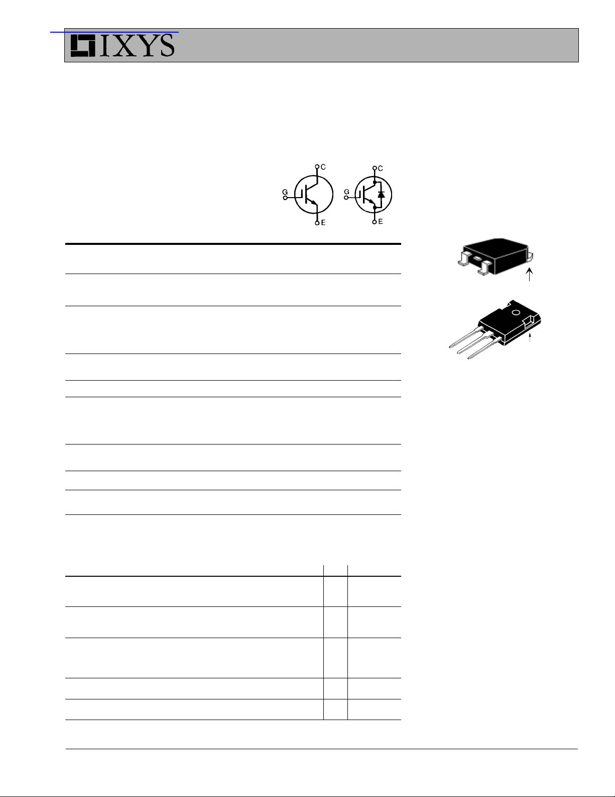
(IXGT)
G
E
C (TAB)
TO-247 AD
(IXGH)
G
C
E
C (TAB)
G = Gate, C = Collector,
E = Emitter, TAB = Collector
Features
z
International standard packages
JEDEC TO-247 AD & TO-268
z
High current handling capability
z
Newest generation HDMOSTM process
z
MOS Gate turn-on
- drive simplicity
Applications
Symbol Test Conditions Characteristic Values
(T
= 25°C, unless otherwise specified)
I
BV
CES
V
GE(th)
I
CES
I
GES
V
CE(sat)
© 2003 IXYS All rights reserved
= 250 µA, V
C
I
= 750 µA 39N60BD1 600
C
I
= 250 µA, V
C
I
= 500 µA 39N60BD1 2.5 5.0 V
C
V
= 0.8 • V
CE
VGE= 0 V T
VCE= 0 V, V
I
= I90, V
C
CES
= ±20 V ±100 nA
GE
= 15 V 1.7 V
GE
J
= 0 V 39N60B 600 V
GE
= V
CE
GE
T
= 25°C 39N60B 200 µA
J
= 125°C 39N60B 1 mA
J
T
= 125°C 39N60BD1 3 mA
J
39N60B 2.5 5.0 V
Min. Typ. Max.
z
PFC circuits
z
AC motor speed control
z
DC servo and robot drives
z
DC choppers
z
Uninterruptible power supplies (UPS)
z
Switched-mode and resonant-mode
power supplies
Advantages
z
High power density
z
Very fast switching speeds for high
frequency applications
DS97548A(02/03)
IXGH39N60B IXGT39N60B
IXGH39N60BD1 IXGT39N60BD1
Symbol Test Conditions Characteristic Values
(T
= 25°C, unless otherwise specified)
g
C
C
C
Q
Q
Q
t
t
t
t
E
t
t
E
t
t
E
R
R
fs
ies
oes
res
G
GE
GC
d(on)
ri
d(off)
fi
off
d(on)
ri
on
d(off)
fi
off
thJC
thCK
J
IC= I
Pulse test, t ≤ 300 µs, duty cycle ≤ 2 %
; VCE = 10 V, 19 28 S
C90
VCE = 25 V, VGE = 0 V, f = 1 MHz 39N60B 200 pF
IC = I
, VGE = 15 V, VCE = 0.5 V
C90
Inductive load, TJ = 25
I
= I
, VGE = 15 V
C
C90
VCE = 0.8 V
, RG = R
CES
°°
°C
°°
= 4.7 Ω
off
CES
Remarks: Switching times may
increase for VCE (Clamp) > 0.8 • V
higher T
Inductive load, TJ = 125
IC = I
V
CE
or increased R
J
, VGE = 15 V
C90
= 0.8 V
CES
, RG = R
G
°°
°C
°°
= 4.7 Ω
off
CES
Remarks: Switching times may
increase for V
higher TJ or increased R
(Clamp) > 0.8 • V
CE
G
CES
min. typ. max.
2750 pF
39N60BD1 240 pF
50 pF
110 150 nC
25 35 nC
40 75 nC
25 ns
30 ns
250 500 ns
,
200 360 ns
4.0 6.0 mJ
25 ns
30 ns
0.3 mJ
360 ns
,
350 ns
6.0 mJ
0.62 K/W
0.25 K/W
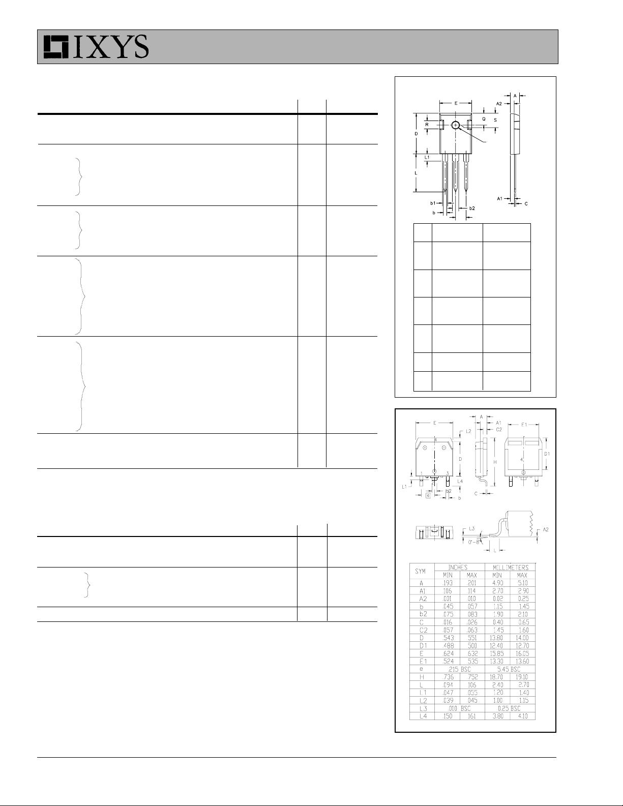
TO-247 AD Outline
Dim. Millimeter Inches
Min. Max. Min. Max.
A 4.7 5.3 .185 .209
A
2.2 2.54 .087 .102
1
A
2.2 2.6 .059 .098
2
b 1.0 1.4 .040 .055
1.65 2.13 .065 .084
b
1
b22.87 3.12 .113 .123
C .4 .8 .016 .031
D 20.80 21.46 .819 .845
E 15.75 16.26 .610 .640
e 5.20 5.72 0.205 0.225
L 19.81 20.32 .780 .800
L1 4.50 .177
∅P 3.55 3.65 .140 .144
Q 5.89 6.40 0.232 0.252
R 4.32 5.49 .170 .216
S 6.15 BSC 242 BSC
∅ P
e
Reverse Diode (FRED) Characteristic Values
(T
= 25°C, unless otherwise specified)
J
Symbol Test Conditions min. typ. max.
V
F
I
RM
t
rr
R
thJC
IF= I
t ≤ 300 µs, duty cycle d ≤ 2 % TJ = 25°C 2.5 V
IF= I
VR= 100 V T
I
IXYS reserves the right to change limits, test conditions, and dimensions.
IXYS MOSFETS and IGBTs are covered by one or more of the following U.S. patents: 4,835,592 4,881,106 5,017,508 5,049,961 5,187,117 5,486,715 6,306,728B1
, VGE = 0 V, Pulse test T
C90
, VGE = 0 V, -di
C90
= 1 A; -di/dt = 100 A/µs; V
F
/dt = 100 A/µs6A
F
= 30 V T
R
=150°C 1.6 V
J
= 100°C 100 n s
J
= 25°C25 ns
J
0.9 K/W
4,850,072 4,931,844 5,034,796 5,063,307 5,237,481 5,381,025

IXGH39N60B IXGT39N60B
IXGH39N60BD1 IXGT39N60BD1
Fig. 1. Saturation Voltage
Characteristics @ 25 Deg. C
40
35
30
25
VGE=15V
13V
11V
9V
7V
20
15
- Amperes
C
I
10
5
5V
0
0.4 0.8 1.2 1.6 2 2.4
V
- Volts
CE
Fig. 3. Saturation Voltage
Characteristics @ 125 Deg. C
100
80
VGE=15V
13V
11V
9V
Fig. 2. Extended Output
Characteristics @ 25 Deg. C
160
140
VGE=15V
13V
11V
120
100
9V
80
60
- Amperes
C
I
40
20
7V
5V
0
012345
VCE - Volts
Fig. 4. Temperature Depende nce of
V
CE(SAT)
1.45
1.3
IC=78A
60
7V
40
- Amperes
C
I
20
5V
0
012345
VCE - Volts
Fig. 5. BV
1.2
1.1
1
- Normalized
(GE)TH
0.9
& V
CES
0.8
BV
0.7
-50 -25 0 25 50 75 100 125 150
CES
& V
vs. Junction
(GE)TH
Temperature
V
GE(T H)
TJ - Degrees Centigrade
BV
CES
1.15
- Normaliz ed
V
CE(SAT)
1
0.85
IC=39A
IC=19.5A
0.7
-50 -25 0 25 50 75 100 125 150
TJ - Degr ees Centigrade
Fig. 6. Admittance
100
80
60
40
- Amperes
C
I
20
TJ= 125°C
°
25
C
°
-40
C
0
456789
V
- Volts
GE
© 2003 IXYS All rights reserved

IXGH39N60B IXGT39N60B
IXGH39N60BD1 IXGT39N60BD1
Fig. 7. Transconductance
50
TJ = -40ºC
25ºC
40
125ºC
30
- Siemens
20
FS
G
10
0
0 20406080100120
Fig. 9. Dependence of E
16
14
12
TJ = 125º C
10
8
- millijoules
6
OFF
E
4
2
0
= 15V
V
GE
V
= 480V
CE
0 102030405060
- Amperes
I
C
R
- Ohms
G
on R
OFF
IC = 78A
IC = 39A
IC = 19.5A
G
Fig. 8. Dependence of E
OFF
on I
16
TJ = 125ºC
14
12
V
V
= 15V
GE
= 480V
CE
RG = 56 Ohms
10
8
- millijoules
OFF
6
E
RG = 5 Ohms
4
2
10 30 50 70 90
- Amperes
I
C
Fig. 10. Dependence of E
OFF
on
Temperature
18
Solid lines - RG = 5 Ohms
Das hed lines - R
15
VGE = 15V
V
12
= 480V
CE
9
- milliJoules
6
OFF
E
3
0
0 25 50 75 100 125 150
T
= 56 Ohms
G
- Degrees Centigrades
J
C
IC =
78A
IC =
39A
IC =
19.5A
Fig. 11. Gate Charge
15
9
6
VCE=300V
I
=20A
C
=10mA
I
G
12
- Volts
CE
V
Fig. 12. Transient Thermal Response
1
(C/W)
0.1
(TH)JC
R
3
0
0 20406080100120
- nanocoulombs
Q
G
0.01
1 10 100 1000
Pulse W idth - m illiseconds
IXYS reserves the right to change limits, test conditions, and dimensions.
IXYS MOSFETS and IGBTs are covered by one or more of the following U.S. patents: 4,835,592 4,881,106 5,017,508 5,049,961 5,187,117 5,486,715 6,306,728B1
4,850,072 4,931,844 5,034,796 5,063,307 5,237,481 5,381,025

IXGH39N60B IXGT39N60B
IXGH39N60BD1 IXGT39N60BD1
60
A
50
I
F
40
TVJ=150°C
30
TVJ=100°C
20
TVJ=25°C
10
0
0123
V
V
F
Fig. 12 Forward current IF versus V
2.0
1.5
K
f
1.0
0.5
I
RM
Q
r
I
RMQ
30
A
25
20
TVJ= 100°C
= 300V
V
R
IF= 60A
IF= 30A
I
F
= 15A
1000
nC
800
r
TVJ= 100°C
VR = 300V
IF= 60A
I
= 30A
F
IF= 15A
600
15
400
10
200
0
100 1000
A/µs
-diF/dt
F
Fig. 13 Reverse recovery charge Q
versus -diF/dt
90
TVJ= 100°C
r
VR = 300V
ns
t
rr
80
5
0
200 600 10000 400 800
/dt
-di
Fig. 14 Peak reverse current I
F
versus -diF/dt
20
TVJ= 100°C
IF = 30A
V
V
FR
15
t
fr
V
FR
A/µs
RM
1.00
µs
t
fr
0.75
IF= 60A
IF= 30A
IF= 15A
10
0.50
70
5
0.25
0.0
0 40 80 120 160
°C
T
VJ
Fig. 15 Dynamic parameters Qr, I
versus T
VJ
RM
60
200 600 10000 400 800
-di
A/µs
/dt
F
Fig. 16 Recovery time trr versus -diF/dt Fig. 17 Peak forward voltage VFR and
1
K/W
0.1
Z
thJC
0.01
0.001
0.00001 0.0001 0.001 0.01 0.1 1
s
t
Fig. 18 Transient thermal resistance junction to case
DSEP 29-06
0
0 200 400 600 800 1000
A/µs
diF/dt
t
fr
Constants for Z
versus diF/dt
calculation:
thJC
iR
(K/W) ti (s)
thi
1 0.502 0.0052
2 0.193 0.0003
3 0.205 0.0162
0.00
© 2003 IXYS All rights reserved
 Loading...