IXYS IXGH 32N60AU1, IXGH 32N60AU1S Service Manual

查询IXGH32N60AU1供应商
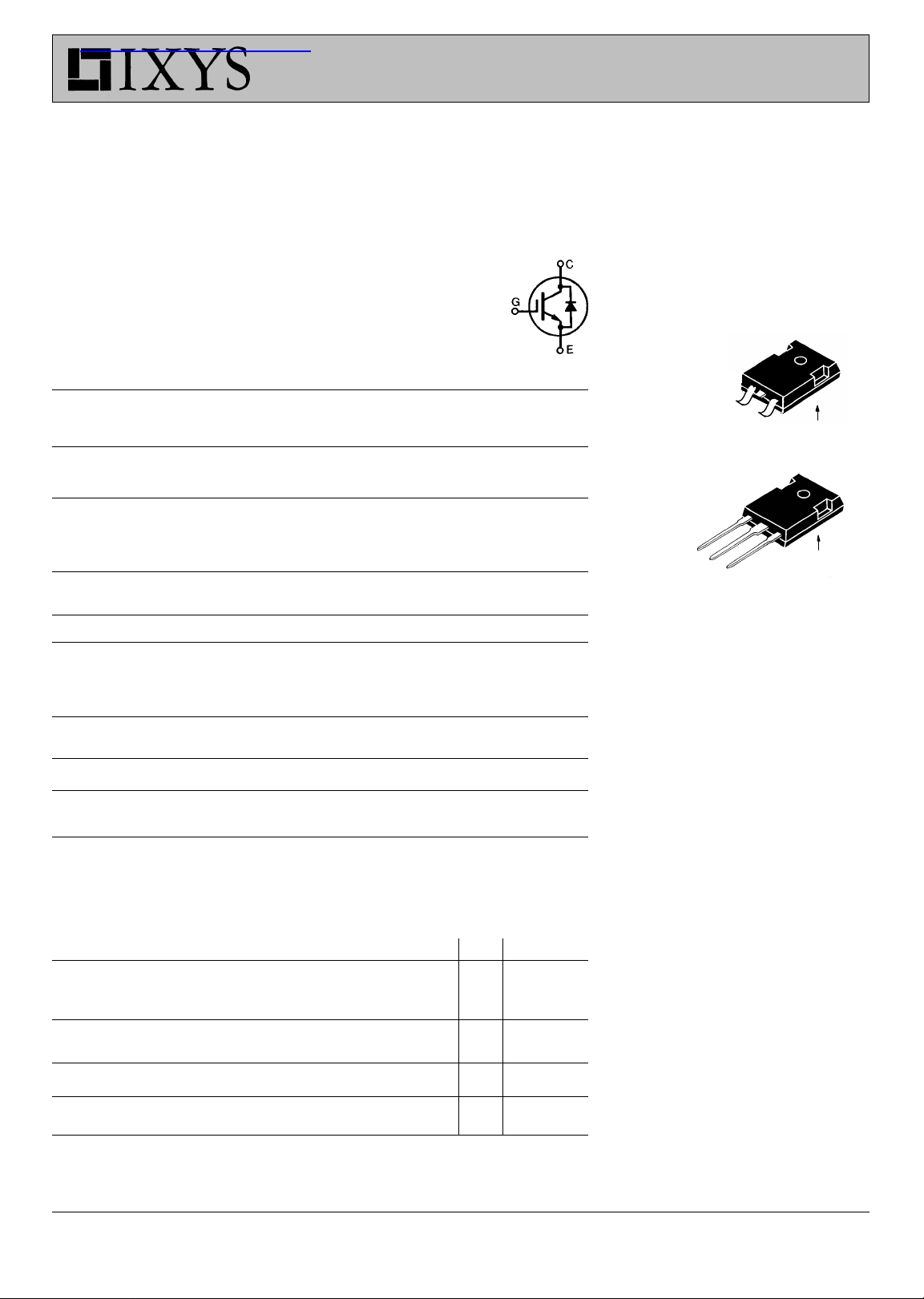
IXGH 32N60AU1
IXGH 32N60AU1S
HiPerFAST
IGBT
with Diode
Combi Pack
Symbol Test Conditions Maximum Ratings
TM
V
CES
V
CGR
V
GES
V
GEM
I
C25
I
C90
I
CM
SSOA V
(RBSOA) Clamped inductive load, L = 100 µH @ 0.8 V
P
C
T
J
T
JM
T
stg
Maximum Lead and Tab temperature for soldering 300 °C
1.6 mm (0.062 in.) from case for 10 s
M
d
Weight TO-247 SMD 4 g
TJ= 25°C to 150°C 600 V
TJ= 25°C to 150°C; RGE = 1 MΩ 600 V
Continuous ±20 V
Transient ±30 V
TC= 25°C60A
TC= 90°C32A
TC= 25°C, 1 ms 120 A
= 15 V, TVJ = 125°C, RG = 33 Ω ICM = 64 A
GE
CES
TC= 25°C 200 W
-55 ... +150 °C
150 °C
-55 ... +150 °C
Mounting torque, TO-247 AD 1.13/10 Nm/lb.in.
TO-247 AD 6 g
V
CES
I
C25
V
CE(sat)
t
fi
= 600 V
= 60 A
= 2.9V
= 125 ns
TO-247 SMD
(32N60AU1S)
G
E
C (TAB)
TO-247 AD
G
C
E
G = Gate C = Collector
E = Emitter TAB = Collector
C (TAB)
Features
●
International standard packages
JEDEC TO-247 SMD surface
mountable and JEDEC TO-247 AD
●
High frequency IGBT and antiparallel
FRED in one package
●
High current handling capability
●
2nd generation HDMOSTM process
●
MOS Gate turn-on
- drive simplicity
Applications
●
AC motor speed control
●
DC servo and robot drives
●
Symbol Test Conditions Characteristic Values
= 25°C, unless otherwise specified)
(T
J
min. typ. max.
DC choppers
●
Uninterruptible power supplies (UPS)
●
Switched-mode and resonant-mode
power supplies
BV
CES
V
GE(th)
I
CES
I
GES
V
CE(sat)
©1996 IXYS Corporation. All rights reserved. 92794H (3/96)
IXYS Corporation
3540 Bassett Street, Santa Clara, CA 95054
Phone: (408) 982-0700 Fax: 408-496-0670
IC= 750µA, VGE = 0 V 600 V
IC= 250 µA, VCE = V
VCE= 0.8 • V
V
= 0 V TJ = 125°C8mA
GE
CES
GE
TJ = 25°C 500 µA
2.5 5.5 V
VCE= 0 V, VGE = ±20 V ±100 nA
IC= I
, VGE = 15 V 2.9 V
C90
Advantages
●
Space savings (two devices in one
package)
●
High power density
●
Suitable for surface mounting
●
Switching speed for high frequency
applications
●
Easy to mount with 1 screw, TO-247
(isolated mounting screw hole)
Edisonstr. 15, D-68623 Lampertheim
Phone: +49-6206-503-0 Fax: +49-6206-503627
IXYS Semiconductor GmbH

IXGH 32N60AU1
IXGH 32N60AU1S
Symbol Test Conditions Characteristic Values
= 25°C, unless otherwise specified)
(T
g
fs
C
ies
C
oes
C
res
Q
g
Q
ge
Q
gc
t
d(on)
t
ri
t
d(off)
t
fi
E
off
t
d(on)
t
ri
E
on
t
d(off)
t
fi
E
off
R
thJC
R
thCK
J
IC= I
Pulse test, t ≤ 300 µs, duty cycle ≤ 2 %
; VCE = 10 V, 15 20 S
C90
VCE = 25 V, VGE = 0 V, f = 1 MHz 270 pF
IC = I
, VGE = 15 V, VCE = 0.5 V
C90
Inductive load, TJ = 25
= I
, VGE = 15 V, L = 100 µH,
I
C
C90
V
CE
= 0.8 V
, RG = R
CES
off
°°
°C
°°
= 4.7 Ω
CES
Remarks: Switching times may
increase for V
higher T
Inductive load, TJ = 125
= I
, VGE = 15 V, L = 100 µH
I
C
C90
= 0.8 V
V
CE
(Clamp) > 0.8 • V
CE
or increased R
J
, RG = R
CES
G
°°
°C
°°
= 4.7 Ω
off
CES
Remarks: Switching times may
increase for V
higher T
(Clamp) > 0.8 • V
CE
or increased R
J
CES
G
min. typ. max.
,
,
2500 pF
70 pF
125 150 nC
23 35 nC
50 75 nC
25 ns
30 ns
120 200 ns
125 175 ns
1.8 mJ
25 ns
35 ns
1mJ
140 ns
260 ns
4mJ
0.62 K/W
0.25 K/W
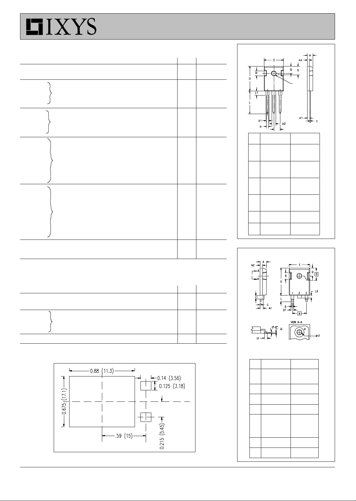
TO-247 AD Outline
e
Dim. Millimeter Inches
Min. Max. Min. Max.
A 4.7 5.3 .185 .209
A
2.2 2.54 .087 .102
1
A
2.2 2.6 .059 .098
2
b 1.0 1.4 .040 .055
b
1.65 2.13 .065 .084
1
2.87 3.12 .113 .123
b
2
C .4 .8 .016 .031
D 20.80 21.46 .819 .845
E 15.75 16.26 .610 .640
e 5.20 5.72 0.205 0.225
L 19.81 20.32 .780 .800
L1 4.50 .177
∅P 3.55 3.65 .140 .144
Q 5.89 6.40 0.232 0.252
R 4.32 5.49 .170 .216
S 6.15 BSC 242 BSC
TO-247 SMD Outline
∅ P
Reverse Diode (FRED) Characteristic Values
= 25°C, unless otherwise specified)
(T
Symbol Test Conditions min. typ. max.
V
F
I
RM
t
rr
R
thJC
IF = I
, VGE = 0 V, 1.6 V
C90
Pulse test, t ≤ 300 µs, duty cycle d ≤ 2 %
IF = I
, VGE = 0 V, -diF/dt = 240 A/µs1015A
C90
VR = 360 V TJ = 125°C 150 ns
I
= 1 A; -di/dt = 100 A/µs; VR = 30 V TJ =25°C35 50ns
F
J
1 K/W
Min. Recommended Footprint
(Dimensions in inches and mm)
IXYS reserves the right to change limits, test conditions, and dimensions.
IXYS Corporation
3540 Bassett Street, Santa Clara, CA 95054
Phone: (408) 982-0700 Fax: 408-496-0670
Phone: +49-6206-503-0 Fax: +49-6206-503627
1. Gate
2. Collector
Dim. Millimeter Inches
Min. Max. Min. Max.
A 4.83 5.21 .190 .205
A1 2.29 2.54 .090 .100
A2 1.91 2.16 .075 .085
b 1.14 1.40 .045 .055
b1 1.91 2.13 .075 .084
C 0.61 0.80 .024 .031
D 20.80 21.34 .819 .840
E 15.75 16.13 .620 .635
e 5.45 BSC .215 BSC
L 4.90 5.10 .193 .201
L1 2.70 2.90 .106 .114
L2 2.10 2.30 .083 .091
L3 0.00 0.10 .00 .004
L4 1.90 2.10 .075 .083
ØP 3.55 3.65 .140 .144
Q 5.59 6.20 .220 .244
R 4.32 4.83 .170 .190
S 6.15 BSC .242 BSC
3. Emitter
4. Collector
IXYS Semiconductor GmbH
Edisonstr. 15, D-68623 Lampertheim
 Loading...